Compact Dual-Band Bandpass Filter Using Embedded
Center-Grounded SIR and Open-Loop Resonators
Jun Li1, *, Shan Shan Huang1, Hui Wang2, and Jian Zhong Zhao1
Abstract—In this article, a compact dual-band bandpass filter (BPF) using coupled open-loop resonators and an embedded center-grounded stepped-impedance resonator (CGSIR) is proposed. This filter operates at 2.1/5.2 GHz for WCDMA/WLAN applications. The first passband is generated by the proposed CGSIR, and the second one is created by the coupled open-loop resonators. Each passband can be controlled independently by adjusting the dimension parameters of corresponding resonators. Five transmission zeros (TZs) are generated due to the 0◦ feed structure and signal cancellation effects between electric couplings and magnetic couplings, which improve the filter band-to-band isolation level and skirt selectivity significantly. Moreover, the overall circuit size is very compact due to the embedded configuration. The measured filter performances are in good agreement with the simulated ones.
1. INTRODUCTION
A multi-band bandpass filter (BPF) is one of the essential components in modern wireless communication systems for multi-band multi-service applications, such as Wideband Code Division Multiple Access (WCDMA) and Wireless Local Area Networks (WLAN) operating at 2.1/5.2 GHz. Great efforts have been made to satisfy the emerging demands, and many multi-band BPFs have been proposed in [1– 10]. Quarter-wavelength stepped-impedance resonators (SIRs) are employed to design dual-band BPFs in [1] and [2]. In [3], configuration of defected ground structure (DGS) is utilized. However, this solution unfortunately increases the insertion loss. Hook-shaped resonators are introduced in [4], two cross-coupled resonators with two quarter-wavelength open stubs generate two passbands. Dual- and tri-band BPFs using asymmetric SIRs with one step discontinuity are proposed in [5] and [6]. The insertion losses are low due to the one step discontinuity, but the center frequencies cannot be controlled individually. Dual-mode ring resonator is proposed in [7] to implement dual-band filter with two transmission poles in both passbands using a single ring resonator. In [8–10], SIRs are used to design dual-band BPFs. Recently, open stub-loaded coupled-line section (OSLCLS) [11], and stub-loaded resonators (SLRs) [12, 13] are proposed to realize dual-/tri-band BPFs.
In this paper, a compact dual-band BPF using open-loop resonators and an embedded center-grounded stepped-impedance resonator (CGSIR) is proposed. The presented CGSIR is short-circuited at the center of a SIR, and it constructs the first passband centered at 2.1 GHz. The second passband centered at 5.2 GHz is formed by the coupled open-loop resonators. Both passbands of the proposed filter can be controlled individually by tuning the dimension parameters of corresponding resonators. In addition, five transmission zeros (TZs) are created due to the 0◦ feed structure and signal cancellation effects between electric couplings and magnetic couplings, which improve the filter band-to-band isolation level and passband selectivity significantly. The design method is validated by a fabricated prototype filter, and the measured results agree well with the simulated ones.
Received 29 July 2014, Accepted 1 September 2014, Scheduled 8 September 2014
* Corresponding author: Jun Li (lijun [email protected]).
1 Ministerial Key Laboratory of JGMT, Nanjing University of Science and Technology, Nanjing 210094, China. 2 28th Research
2. DUAL-BAND BPF DESIGN
2.1. Resonators Analysis
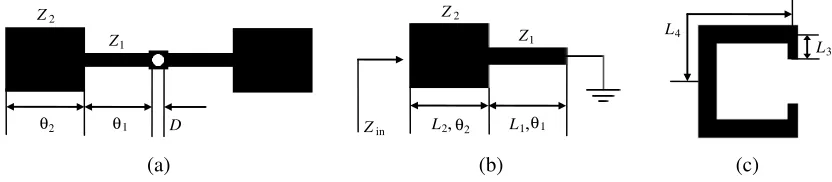
Figure 1(a) shows the layout of the proposed CGSIR, and Figure 1(b) shows the conventional quarter-wavelength SIR. Z1 and Z2 are the characteristic impedances of high- and low-impedance sections,
and θ1 and θ2 are the corresponding electrical lengths, respectively. The proposed CGSIR can be seen
as two conventional quarter-wavelength SIRs connected with a common short-ended via hole which is characterized by diameterD. As discussed in [1], the via hole can be seen as a semi-lumpedK-inverter, and the two quarter-wavelength SIRs are inductively coupled with each other.
L2, L1,
Z D
Z2
Z1
L4
L3
(a) (b) (c)
Z2
Z1
in
θ2 θ1 θ2 θ1
Figure 1. (a) Layout of the proposed CGSIR. (b) Layout of the conventional quarter-wavelength SIR. (c) Layout of the open-loop resonator.
Since the proposed CGSIR is composed by two inductively coupled quarter-wavelength SIRs as depicted in Figure 1(b), the resonant frequencies of the CGSIR can be obtained by solving the resonant condition Zin=∞of the quarter-wavelength SIR. The input impedance is
Zin =jZ2
Z1tanθ1+Z2tanθ2
Z2−Z1tanθ1tanθ2
. (1)
By employing the resonant condition, the following equations can be obtained
Z2−Z1tanθ1tanθ2 = 0 (2)
K = Z2
Z1
= tanθ1tanθ2 (3)
where K is the impedance ratio of low- and high-impedance sections. As shown in Figure 1(b), it is open-circuited at one end and short-circuited at the other end. Thus, it acts as a quarter-wavelength resonator, which resonant frequencies can be approximately derived by Equation (4) [6]
f1≈
c
4(L1+L2)√εeff1
(4)
where c is the speed of light in free space, and L1 and L2 are the physical lengths of high- and
low-impedance lines, respectively.
εeff1 =
εr+ 1 2 +
εr−1 2
1 + 12 h
w1
−1/2
+ 0.04
1− w1
h
2
(5)
is the effective dielectric constant. h is the thickness of substrate, and parameter w1 can be estimated
as
w1 =
w1+w2
2 (6)
wherew1 and w2 are the widths of high- and low-impedance sections, respectively. Thus, the resonant
characteristics of the proposed CGSIR is clear, and the center frequency of the first passband can be obtained by Equations (1)–(6), and can be controlled by changing the values ofL1 and L2.
J-inverter which is realized by a coupling gap. Therefore, the couplings between them are electric couplings. According to reference [6], the open-loop resonators act as half-wavelength resonators which resonant frequencies can be approximately calculated by
f2 ≈
c
2 (2L3+ 2L4)√εeff2
(7)
whereεeff2 is the dielectric constant calculated by (5) using the average width w2 = (w3+w4)/2, and
L3,L4andw3,w4 are the physical lengths and widths of the high- and low-impedance sections as shown
in Figure 1(c), respectively. Therefore, center frequency of the second passband is determined by (7) and can be controlled by tuning the values ofL3 and L4.
2.2. Filter Design
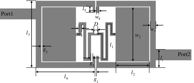
Based on the above analysis, a dual-band BPF is designed for 2.1/5.2 GHz WCDMA/WLAN applications. The specific configuration of the proposed dual-band BPF is depicted in Figure 2. As can be seen from Figure 2, this filter consists of two sets of resonators, namely, CGSIR and open-loop resonators. And CGSIR is embedded in the coupled open-loop resonators, which leads to a compact circuit size. The former resonator is used to generate the first passband centered at 2.1 GHz, and the latter is applied to obtain the second passband centered at 5.2 GHz. A pair of 50 Ω I/O ports is tapped at the open-loop resonators using a 0◦ feed structure.
Port1
Port2 l3
l4 l2
l1
lt w3 w2 w1
w4
g
3
g
2
g
1
l5
D
Figure 2. Configuration of proposed dual-band BPF (l1 = 9.85 mm, l2 = 3.6 mm, l3 = 7.2 mm,
l4 = 6.35 mm, l5 = 0.67 mm, lt = 1.98 mm, w1 = 0.3 mm, w2 = 5.8 mm, w3 = 0.6 mm, w4 = 0.25 mm,
g1= 0.1 mm, g2 = 0.1 mm,g3 = 0.2 mm, andD= 0.4 mm).
As discussed above, the CGSIR is composed by two inductively coupled quarter-wavelength SIRs through a via hole (K-inverter), and the two open-loop resonators are capacitively coupled with each other through a coupling gap (J-inverter). Therefore, the mainline paths for signals from port 1 to port 2 are J-K-J, and the out-of-phase cancellation effect occurs at the first passband, resulting in a pair of TZs at both sides of the first passband [1]. In addition, two TZs are created at both sides of the second passband due to the 0◦ feed structure. Thus, the stopband rejection and skirt selectivity of both passbands are significantly improved.
Figure 3 depicts the extracted external quality factors (Qe) of both passbands with varied tapped position of I/O ports (lt) and diameter of via hole (D). It is clear from Figure 3 that Qe of the second passband increases withltwhile the first one is almost unchanged. In addition, diameter of the via hole,
D, has little influence onQe of both passbands. Figure 4 shows the extracted coupling coefficients (K) of both passbands with varied coupling gap (g1) andD. As can be seen from Figure 4,K of the second
passband decreases with the increase of g1, while the first one keeps constant. Moreover, diameter D
only affects K of the first passband without influencing the second one, and the larger the diameter
D is, the stronger the coupling coefficient of the first passband is. Therefore, Qe and K of the two
1.50 1.75 2.00 2.25 2.50 0
10 20 30 40
Qe
lt (mm)
Band 1 Band 2
Figure 3. Extracted external quality factor (Qe) with varied lt and D. (Solid line: D = 0.4 mm; dash line: D= 0.5 mm).
0.1 0.2 0.3 0.4
0.00 0.02 0.04 0.06 0.08 0.10 0.12
K
g 1 (mm)
Band 1 Band 2
Figure 4. Extracted coupling coefficient (K) with varied g1 and D. (Solid line: D = 0.4 mm;
dash line: D= 0.5 mm).
3. SIMULATED AND MEASURED RESULTS
In order to demonstrate the validity of the above-mentioned design method, a compact dual-band BPF is designed and fabricated on a Rogers RO4003 substrate with a thickness of 0.508 mm, a dielectric constant εr of 3.55, and a loss tangent of 0.0027. The simulations are carried out by using a full-wave electromagnetic (EM) simulator ANSYS HFSS V15, and measurements are performed with an Agilent’s N5244A network analyzer.
The dimensions are optimized as follows: l1 = 9.85 mm, l2 = 3.6 mm,l3 = 7.2 mm, l4 = 6.35 mm,
l5 = 0.67 mm, lt = 1.98 mm, w1 = 0.3 mm, w2 = 5.8 mm, w3 = 0.6 mm, w4 = 0.25 mm, g1 = 0.1 mm,
g2 = 0.1 mm, g3 = 0.2 mm, andD= 0.4 mm. The overall circuit size only occupies 7.2 mm×12.8 mm,
i.e., approximately 0.08λg×0.146λg, where λg is the guided wavelength at the center frequency of the
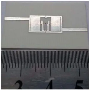
first passband (2.1 GHz). It is clear that the proposed BPF is very compact in size. It is noted that the size of dual-band BPF proposed in this work is about 93.3% reduction in comparison with the one proposed in [5]. A photograph of the fabricated prototype dual-band BPF is shown in Figure 5.
The simulated and measured frequency responses are shown in Figure 6, which reveals that the measured results are in good agreement with the simulated ones. The measured center frequencies are 2.1 and 5.19 GHz with 3 dB fractional bandwidths (FBWs) of 5.7%, and 11.9%, respectively. The minimum insertion losses (IL) are 1.12 and 0.98 dB while the return losses (RL) are better than 20 and 23 dB. The isolation level between the two passbands is around 23 dB. Five TZs are generated at 0,
Figure 5. Photograph of the fabricated dual-band BPF.
|S |11
|S |21
Simulated Measured
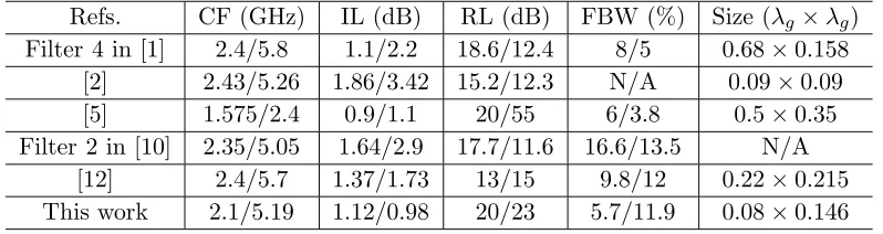
Table 1. Comparison of the proposed filter with some reported works.
Refs. CF (GHz) IL (dB) RL (dB) FBW (%) Size (λg×λg)
Filter 4 in [1] 2.4/5.8 1.1/2.2 18.6/12.4 8/5 0.68×0.158 [2] 2.43/5.26 1.86/3.42 15.2/12.3 N/A 0.09×0.09 [5] 1.575/2.4 0.9/1.1 20/55 6/3.8 0.5×0.35 Filter 2 in [10] 2.35/5.05 1.64/2.9 17.7/11.6 16.6/13.5 N/A
[12] 2.4/5.7 1.37/1.73 13/15 9.8/12 0.22×0.215 This work 2.1/5.19 1.12/0.98 20/23 5.7/11.9 0.08×0.146
(CF, IL, RL, and FBW denote center frequencies, insertion losses, return losses, and fractional bandwidths, respectively.)
1.86, 2.3, 4.31, and 6.49 GHz, which suppress DC signals and improve band-to-band isolation level and passband selectivity greatly.
Table 1 gives a comparison between this work and some previous works reported in [1, 2, 5, 10, 12]. It can be seen that the proposed dual-band BPF has merits of compact circuit size (about 93.3% reduction comparing with [5]), low insertion loss, high skirt selectivity and band-to-band isolation level, reasonable bandwidths, and independently controllable center frequencies and FBWs.
4. CONCLUSION
In this paper, a compact dual-band BPF operating at 2.1 and 5.2 GHz for WCDMA and WLAN applications is introduced and analyzed. By using a pair of open-loop resonators and a CGSIR, two passbands are generated and can be controlled individually. In addition, five TZs are created by utilizing the signal cancellation effects between electric and magnetic couplings and the 0◦ feed structure. These five TZs are located at DC and close to the passband edges, which improve the skirt selectivity and band-to-band isolation level of the proposed filter significantly. It is worth mentioning that the proposed dual-band BPF is very compact with a circuit size of only 0.08λg ×0.146λg due to the embedded configuration. Good agreement between the simulated and measured results is achieved. All the merits indicate that this filter is very suitable for modern wireless communication systems.
REFERENCES
1. Zhang, S. and L. Zhu, “Synthesis design of dual-band bandpass filters withλ/4 stepped-impedance resonators,”IEEE Trans. Microw. Theory Tech., Vol. 61, No. 5, 1812–1819, May 2013.
2. Wei, X. B., Y. Shi, P. Wang, J. X. Liao, Z. Q. Xu, and B. C. Yang, “Compact dual-band bandpass filter with improved stopband characteristics,” Electron. Lett., Vol. 48, No. 12, 704–705, 2012. 3. Mohan, A. and A. Biswas, “Dualband bandpass filter using defected ground structure,” Microw.
Opt. Technol. Lett., Vol. 51, No. 2, 475–479, Feb. 2009.
4. Zhang, Z., et al., “Design of a compact dual-band bandpass filter using opposite hook-shaped resonator,” IEEE Trans. Microw. Wireless Compon. Lett., Vol. 21, No. 7, 359–361, Jul. 2011. 5. Chang, Y. C., et al., “Design of the compact dual-band bandpass filter with high isolation for
GPS/WLAN applications,” IEEE Trans. Microw. Wireless Compon. Lett., Vol. 19, No. 12, 780– 782, Dec. 2009.
6. Li, J., S. S. Huang, and J. Z. Zhao, “Design of a compact and high selectivity tri-band bandpass filter using asymmetric stepped-impedance resonators (SIRs),” Progress In Electromagnetics Research Letters, Vol. 44, 81–86, 2014.
8. Wang, J., et al., “High-selectivity dual-band stepped-impedance bandpass filter,” Electron. Lett., Vol. 42, No. 9, 538–540, Sep. 2006.
9. Kuo, J. T., T. H. Yeh, and C. C. Yeh, “Design of microstrip bandpass filters with a dual-passband response,”IEEE Trans. Microw. Theory Tech., Vol. 53, No. 4, 1331–1337, Apr. 2005.
10. Guo, L., Z.-Y. Yu, and L. Zhang, “Design of a dual-mode dual-band filter using stepped impedance resonators,”Progress In Electromagnetics Research Letters, Vol. 14, 147–154, 2010.
11. Xu, J. and W. Wu, “Miniaturised dual-wideband bandpass filter using novel dual-band coupled-line sections,” Electron. Lett., Vol. 49, No. 18, 1162–1163, Aug. 2013.
12. Chen, F.-C. and J. M. Qiu, “Third-order dual-band bandpass filter with controllable bandwidths using short stub-loaded resonators,” Progress In Electromagnetics Research Letters, Vol. 32, 101– 108, 2012.