© 2018, IRJET | Impact Factor value: 6.171 | ISO 9001:2008 Certified Journal | Page 1070
DC Variable Electronic load for SMPS Testing
G A Rathy
1, Aravind balaji
21Associate Professor, Electrical Department, NITTTR, Chennai, India
2R&D Engineer, Bharathi Enterprises, Chennai, India
---***---Abstract - As technology is constantly advancing, demands
for quality test instruments increase due to the need for making better and accurate measurements to accommodate newer technologies. DC Electronic loads are one such instrument that will aid in testing various settings, configurations, schemes, and methodologies The intention of this application note is to provide a general scope of a DC load's usage. As regulated-power supply technology evolves, testing methods for design verification and product function require more sophisticated electronic equipment. The different power supply architectures and output combinations also dictate the need for versatile test instruments that can accommodate a broad range of specifications. As a result, one testing requirement that has been growing in importance is the method of loading the power supply under test. The need for a higher degree of load control is due to test sophistication. Thus this paper presents a Variable electronic load using MOSFET switching to load the SMPS.
Key Words: SMPS, Electronic load, MOSFET, test instruments.
1. INTRODUCTION
The Electronic loads have found a variety of applications ranging power converter testing to current modulation. A large range of power sources can be tested using an electronic load from converters, inverters and UPSs to electrochemical sources such as batteries and fuel cells. They are easy-to-use and provide much higher throughput than resistors when varying loads are needed. For battery test, they provide a constant loading which can greatly reduce the time for test when compared to resistor load banks. Electronic loads can also simulate various power states of a device such as a handheld which may have sleep, power conservation and full power modes. They also present a complex electronic load which more closely simulates the real environment of the power source. Modulation uses improve the performance of programmable power supplies by providing faster transient response.
1.1 .SMPS
The multiple DC voltage levels required by many electronic devices, designers need a way to convert standard power-source potentials into the voltages dictated by the load. Voltage conversion must be a versatile, efficient, reliable process. Switch-mode power supplies (SMPSs) are frequently used to provide the various levels of DC output power needed for modern applications, and are indispensable in achieving
highly efficient, reliable DC-DC power-conversion systems. SMPSs can convert a DC input voltage into a different DC output voltage, depending on the circuit topology. While there are numerous SMPS topologies used in the engineering world, three are fundamental and seen most often. These topologies are classified according to their conversion function: down (buck), up (boost), and step-up/down (buck-boost or inverter). All three fundamental topologies include a MOSFET switch, a diode, an output capacitor, and an inductor. The MOSFET, which is the actively controlled component in the circuit, is interfaced to a controller. This controller applies a pulse-width-modulated (PWM) square-wave signal to the MOSFET's gate, thereby switching the device on and off. To maintain a constant output voltage, the controller senses the SMPS output voltage and varies the duty cycle (D) of the square-wave signal, dictating how long the MOSFET is on during each switching period (TS).
1.2. ELECTRONIC LOAD
Electronic loads provide a very fast method to test converters of all types DC-DC, AC-DC and DC-AC. Load regulation, over current protection, noise testing (with appropriate filtering), and overpower protection can all be very quickly tested in a laboratory or production environment. The flexibility in operating range of the electronic load also allows a quick verification of power supply ratings.Electronic loads can be used to directly test the capacity of a battery. This can be done in constant power mode (CP) to provide a consistent drain that does not change as the battery voltage drops. Electronic loads are also used in battery forming operations as part of the charge/discharge cycling.With the constant drive to find high power density batteries for both handheld applications and hybrid vehicles, battery controller development and test are a common application for electronic loads. As discharge profiles are specific to a particular battery design and/ or charge state, the ability of a load to produce quick changes in load are essential for this application.
© 2018, IRJET | Impact Factor value: 6.171 | ISO 9001:2008 Certified Journal | Page 1071 electronic loads also feature constant resistance (CR)
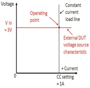
operation as well. Many real-world loads are resistive by nature and hence it is often useful to test power sources meant to drive such devices with an electronic load operating in CR mode. The CC and CV modes are very similar in operation for both a power supply and an electronic load. An electronic load CC mode operation is depicted in Figure below.
Fig -1: CC Mode operation
The load, operating in CC mode, is loading the output of an external voltage source as shown in Figure1. The current amplifier is regulating the electronic load’s input current by comparing the voltage on the current shunt against a reference voltage, which in turn is regulating how hard to turn on the load FET. The corresponding I-V diagram for this CC mode operation is shown in Figure 2 . The operating point is where the output voltage characteristic of the DUT voltage source characteristic intersects the input constant current load line of the electronic load.
Fig -2: Electronic load V-I diagram
CV mode is very similar to CC mode operation, as depicted in Figure 3. However, instead of monitoring the input current with a shunt voltage, a voltage control amplifier compares the load’s input voltage, usually through a voltage divider, against a reference voltage. When the input voltage signal reaches the reference voltage value the voltage amplifier turns the load FET on as much as needed to clamp the voltage to the set level.
Fig -3: CV Mode operation
A battery being charged is a real-world example of a CV load, charged typically by a constant current source. The corresponding I-V diagram for CV mode operation is depicted in Figure 4.
Fig -4: Electronic load I-V diagram
1.3. ANALOG COMPARATOR
The Op-amp comparator as shown in Figure 5 compares one analogue voltage level with another analogue voltage level, or some preset reference voltage, VREF and produces an output signal based on this voltage comparison. In other words, the op-amp voltage comparator compares the magnitudes of two voltage inputs and determines which is the largest of the two. Voltage comparators on the other hand, either use positive feedback or no feedback at all (open-loop mode) to switch its output between two saturated states, because in the open-loop mode the amplifiers voltage gain is basically equal to AVO. Then due to this high open loop gain, the output from the comparator swings either fully to its positive supply rail, +Vcc or fully to its negative supply rail, -Vcc on the application of varying input signal which passes some preset threshold value.
[image:2.595.355.523.93.184.2] [image:2.595.92.276.196.317.2] [image:2.595.360.507.301.405.2] [image:2.595.83.232.492.638.2]© 2018, IRJET | Impact Factor value: 6.171 | ISO 9001:2008 Certified Journal | Page 1072
Fig -5: Analog comparator
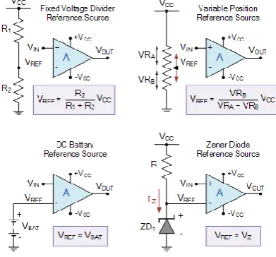
With reference to the op-amp comparator circuit above, lets first assume that VIN is less than the DC voltage level at VREF, ( VIN < VREF ). As the non-inverting (positive) input of the comparator is less than the inverting (negative) input, the output will be LOW and at the negative supply voltage, -Vcc resulting in a negative saturation of the output. increase the input voltage, VIN so that its value is greater than the reference voltage VREF on the inverting input, the output voltage rapidly switches HIGH towards the positive supply voltage, +Vcc resulting in a positive saturation of the output. If we reduce again the input voltage VIN, so that it is slightly less than the reference voltage, the op-amp’s output switches back to its negative saturation voltage acting as a threshold detector.depending upon the circuit as shown in the figure 6 the reference voltage can be calculated. It can be determined between 0 to VCC.
Fig -6: Comparator Reference voltage
2. CIRCUIT IMPLEMENTATION
The basic SMPS loading circuit is illustrated below in which the electronic load is in parallel with the SMPS and the load current Iload flows across the load and SMPS
Fig -7: Basic Load circuit
The Figure7 given below shows the circuit diagram of the power circuit of the DC electronic load in which regulated +12v is been generated using a rectifier and a regulator which are been provided as an power source for the comparator here operational amplifier is been used as analog comparator.thermister are been provided to monitor the temperature and if it’s not of desired temperature fan out are been provided to turn on the fan using a transistor which acts as an switch. As far as control circuit is concern it is used to switch the MOSFET depending upon the load current id required the figure given below shows the control circuit in which MOSFET is been switch on depending upon the analog comparator output.
Fig 8: Power circuit
[image:3.595.67.263.96.232.2] [image:3.595.320.549.100.177.2] [image:3.595.305.567.379.738.2] [image:3.595.76.272.478.660.2]© 2018, IRJET | Impact Factor value: 6.171 | ISO 9001:2008 Certified Journal | Page 1073 The power circuit and control circuit shown in Figure 8 &9
can provide up to 6A of load current, this is achieved by using six MOSFET switch Q1 to Q6 in which each MOSFET provide 1A of load totally providing 6A using those MOSFET. LM358 which act as an analog comparator is used to compare the reference voltage with the input voltage which varies from 0 to 1V. Hence varies the switching time of the MOSFET which varied the load current across each MOSFET. The reference voltage is been varied depending upon the 10K load control potentiometer is used for varying the load current as required.
The load input voltage is limited mainly by the drain to source voltage (Vds) rating of the MOSFET, and current by the value of current sense resistor. Take note, while connecting the source to the load, you should calculate the power dissipation carefully to retain the MOSFET always in the safe operating area (SOA) otherwise it will be deep-fried as soon as its die temperature exceeds the safety margin. Regarding heatsink selection for the MOSFET, a standard TO-247AC type with a thermal resistance of 0.24C/W should be a good pick. Since the typical junction-to-case thermal resistance of MOSFET IRF250 is 1.00C/W, case-to-sink thermal resistance is 0.24C/W, and maximum operating temperature range of 1750 C, the maximum power dissipation allowed will be 1750C – 25 0C (ambient temperature) / 40 C/W (total thermal resistance) around 37W. Similarly, try to use a 1R/10W-50W aluminum clad power resistor as the current sense resistor. If possible opt for the better TO-220 type power resistor (naturally with a heatsink) as it’s more convenient and efficient. Also, it’s good to attach a digital ammeter in to the load path, to measure the current drawn from the source.
[image:4.595.336.531.141.270.2]3. HARDWARE IMPLEMENTATION
Fig -10: Hardware Implementation
The figure10 given below shows the hardware implementations of the electronic load in which IRF250 MOSFET are been used with proper heat sink and cooling fan to dissipate the heat induced due to loading effect. Current meter are been provided to indicate the current and ten turn potentiometer are been used to get a precise value of
variation between desired load current. Metal casing are been provided to reduce shock and physical damage.
3.RESULT
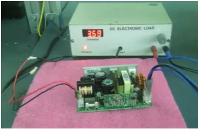
Fig -11: Result
The figure 11 shows the verification of the DC load output in which a 24V SMPS is been loaded with the electronic load . AC input is been applied to one end of the SMPS and the load is been connected to the output of the SMPS. By varying the potentiometer the output load current current can be varied from 0 to 6A here in the figure the SMPS is been loaded with 3.6A load.
4. CONCLUSIONS
Thus this paper presents the implementation of the DC variable electronic load in which by using the MOSFET as the load to provide the desired current the output load current can be varied upto 6A. The number of MOSFET can be increased to increase the output load current for which desired reverse current protection circuits and high current rated MOSFET are to be used. Proper heat sinking method is to be followed to dissipate excess heat.
REFERENCES
[1] Kazerani, M., “A High-Performance Controllable DC
Load”, IEEE International Symposium on Industrial Electronics, ISIE 2007, pp. 1015-1020, June, 2007.
[2] Durán, E., Andújar, J.M., Segura, F., Barragán, A.J., “A
High-Flexibility DC Load for Fuel Cell and Solar Arrays power sources based on DC–DC converters”, Applied Energy, Vol. 88, Issue 5, pp. 1690-1702, May 2011.
[3] Canesin, C.A., Seixas, F.J.M., Seixas, C.M., “A 300A
Dynamic Electronic Load Based On Modified Buck-Boost Interleaved Converter”, Eletrônica de Potência, Vol. 11, No. 3, pp. 161-166, 2006.
[4] Kuai, Y., Yuvarajan, S., “An Electronic Load for Testing
[image:4.595.64.262.506.651.2]© 2018, IRJET | Impact Factor value: 6.171 | ISO 9001:2008 Certified Journal | Page 1074
[5] Huilin, O., Gang, W., “The Study of Electronic Load Based
on DSP”, First International Conference on Power Electronics Systems and Applications, pp. 285-290, November 2004.
[6] Zhu Jingang, “Design of Intelligent Electronic
Load,”Experimental Technology and Management, Vol. 06, pp. 27-29, 58, 2006.
[7] [2] Gao Jiaying, Gao Yufeng, and Liu Yalong, “Research of
constant-current Discharge Equipment with New Type Electronic Load,”
[8] w.amrel.com /AMRELPowerProducts/index.html. .
[9] [7] B&K Precision Corporation, "150 DC Electronic
Load," November 2008. [Online].Available:
[10] http://www.bkprecision.com/products/model/8540/