Simulation & Analysis of Diode Clamped
and Modular Multilevel Inverters
Using Sinusoidal PWM
Manju Ann Mathews1, Akhila.A2
Assistant Professor, Dept. of EEE, Mar Baselios College of Engineering and Technology, Trivandrum, Kerala, India1
PG Student [PCD], Dept. of EEE, Mar Baselios College of Engineering and Technology, Trivandrum, Kerala, India2
ABSTRACT: Multilevel inverters are considered as the best option for use in high power and medium voltage applications due to their minimum harmonic distortion, reduced EMI and EMC issues, reduced dv/dt stresses and also their ability to operate in several voltage levels. This paper presents the analysis and comparison of a conventional three level Diode clamped or Neutral point clamped multilevel inverter and modular multilevel converter (MMC) topologies. The PWM technique used here is Sinusoidal PWM (SPWM). For the two topologies mentioned, simulations are carried out for both inductive and resistive loads. By comparing the THDs, the advantages of the modular multilevel converters over the conventional inverters are confirmed. The simulations are performed using MATLAB/SIMULINK software and the results are presented.
KEYWORDS:Multilevel inverters(MLI),NPC,THD,SPWM, Modular Multilevel Converter(MMC).
I.INTRODUCTION
Inverter is a device which converts DC power to AC power at desired voltage and frequency level. These are broadly classified into single level inverters and multilevel inverters. Multilevel converters are now a day considered as one of the industrial solutions for high dynamic performance and power quality demanding applications. Multilevel converters are the power conversion systems composed of an array of power semiconductor devices and the capacitive voltage sources that can be connected and controlled properly for generating a multistep voltage waveform with variable and controllable frequency, phase and amplitude. That is the sine wave can be approximated to a stepped waveform having larger number of steps. The number of levels of an inverter is defined as the number of steps or constant voltage values that can be generated by the converter between the output terminal and an arbitrary reference node called the neutral. Comparing with the two level inverters of the same power rating, multilevel inverters have the advantages of low switching frequency and hence reduction in the switching losses, reduced EMI issues and also reduction in the harmonic components of the line to line voltages etc. The major multilevel converter topologies are [4]-[5]:
Diode clamped or neutral point clamped
Flying capacitor or capacitor clamped.
Cascaded multilevel inverters with isolated dc sources.
Among the three different topologies mentioned above the diode clamped or neutral point clamped(NPC) has been commonly used. However, it is difficult to control the real power flow for balancing the neutral point potential. The advantages of multilevel converters are the staircase waveform quality, lower or reduced common mode voltages, can operate at both fundamental and high switching frequency PWM, reduced switching stresses on devices etc. [1]-[3]. Recently, the modular multilevel converter (MMC) topology has become an alternative to the conventional multilevel inverters in medium and high voltage applications. The MMC consists of series connected half bridges with dc capacitors called as the sub modules. Each phase leg consists of one upper arm and one lower arm connected between the dc terminals. The advantages of modular multilevel converter over the conventional multilevel inverters are:
Modular construction
As number of levels increases, interface transformer an output filter can be eliminated, resulting in significant reduction in cost.
No bulk DC capacitor is needed and the energy is distributed along the different capacitors at each cell.
II.REVIEW OF DIODE CLAMPED ND MODULAR MULTILEVEL CONVERTERS A. DIODE CLAMPED MULTILEVEL INVERTER
The topology of three phase three level diode clamped or neutral clamped multilevel inverter is shown in the figure 1.It is similar to that of a two level inverter stacked one over the other with certain modifications.[2] This topology consists of twelve switches Each leg consists of four switches. Considering A phase the switches Sa1 and Sa3 are complementary and the other complementary pairs are Sa2 and Sa4.For m levels (m-1) capacitors,(m-1)(m-2) clamp diodes and 2(m-1)switches and parallel diodes are required .Considering A phase for obtaining a positive voltage switches Sa1 and Sa2 are ON and for negative voltage switches Sa3 and Sa4 are ON and for getting zero level the middle switches Sa2 and Sa3are operated. Considering figure 1 ic1 and ic2 be the current in the upper and lower
Fig.1 Schematic of three phase three level diode clamped multilevel inverter Capacitors C1 and C2respectively.SupposeC1=C2 =C, ic1,ic2 and io can be derived as follows:
1 = ………..…...(1)
2 = …..………...(2)
0 = 1− 2………....(3)
0 =−2 ……...………...(4)
The PWM used here is SPWM. Va,Vb and Vc are the three phase reference voltages which are displaced at1200 apart.
The triangular wave is used as the carrier wave. The reference signal is having a frequency of 50Hz and the carrier signal is having a switching frequency of 10 KHz. Both the signals have the same amplitude of 1V.The switching pulses is in such a way that in each phase the first and the third switches are complementary and the second and fourth switches are complementary. The carriers for the first and the second switches are1800 out of phase and the third and fourth switches are having a phase shift of 1800.
B. MODULAR MULTILEVEL CONVERTER
compensate for the voltage difference produced between the upper and lower arms when a sub module is switched in or out. For the inverter operation the ac side current iac and the line to neutral voltage vac are given by:
iac=iacCos(ωt+Ø) ………...(5)
vac=vacCos (ωt)………(6)
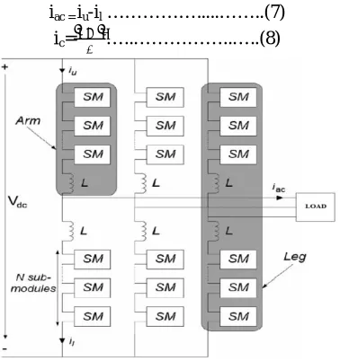
where ω is the angular fundamental frequency. The currents flowing in the arms are termed as the arm currents. As shown in the figure 2 a positive arm current is flowing from the positive dc terminal to the ac terminal and a positive lower arm current is flowing from the ac terminal to the negative dc terminal. The mean value ic of the upper and lower
arm current is termed as the circulating current. Let iu and il be the upper and lower arm currents respectively, they must
satisfy the following equations:
iac = iu-il ………...……..(7)
ic= …..………..…..(8)
Fig.2 Schematic of three phase three level modular multilevel converter Solving equations (7)and (8)
iu=ic+ iac Cos(ωt+Ø)……..(9)
il=ic- iac Cos(ωt+Ø)…...(10)
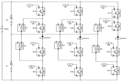
Figure 3 shows the schematic of one phase of a three level modular multilevel converter. It consists of four main switches(Sa1,Sa2,Sa3 and Sa4) and four auxiliary switches (Sx1,Sx2,SX3 and Sx4).There are four complementary switch pairs per phase that is (Sa1,Sx1),(Sa2,Sx2), (Sa3,Sx3) and (Sa4.Sx4).in each instant four switches must be in ON state two from the main switches and two from the auxiliary switches. The voltage stress on each switching devices is limited to one capacitor voltage. For obtaining voltage level Vao=1/2 Vdc the upper switches Sa1 and Sa2 ON
and the lower auxiliary switches Sx3, Sx4 ON. For voltage level Vao=-1/2 Vdc the upper switches Sa3 and Sa4 ON. And
lower auxiliary switches Sx1,Sx2 ON. For getting zero voltage level four different switching combinations are possible:
(a)Turn ON switches Sa1,Sa3,Sx2 andSx4 (b)Turn ON switches Sa2,Sa3, Sx1 andSx4 (c)Turn ON switches Sa2,Sa4, Sx1 andSx3 (d)Turn ON switches Sa1,Sa4, Sx2 andSx3
Fig.3 Schematic of one phase of three level modular multilevel converter
1V and frequency 50Hz which are displaced at 1200 apart and two triangular carrier waves which are displaced at 1800 apart per phase the amplitude of the carriers are 1V and the switching frequency is 10KHz.Considering phase A the sine reference and the first carrier are compared and the output pulses are fed to the switches Sa1 and Sx4 and the complementary pulses from the NOT gate are fed to Sa4 and Sx1.Then the sine reference and the second carrier which is displaced at 1800 with the first carrier are compared and the corresponding pulses are fed to switches Sa2 and Sx3 and the complementary pulses from the NOT gate are fed to switches Sa3 and Sx2.
III. RESULT AND DISCUSSION
The comparison of diode clamped and modular multilevel converters are conducted using MATLAB/SIMULINK. Here the sinusoidal pulse width modulation (SPWM) with switching frequency of 10 KHz is used as the basic modulation for both the converters. The output load current voltages and Total harmonic distortion is obtained for different inverter topologies using the load values as R=1Ω,L=5.4mH,input DC source voltage 800V and dc link capacitors each 4700µF.
A .THREE LEVEL(NPC) INVERTER In the figure 4,it shows the simulink model of diode clamped MLI.
.
In the fig 5, it shows three level NPC simulink model,
Fig.5.Three level Diode clamped multilevel inverter Simulink Model
Fig 6.Sinusoidal PWM
In the figure 6,it shows the sinusoidal PWM of diode clamped MLI. Figure 7,it shows the output line voltage.
Fig7.Inverter output line voltage
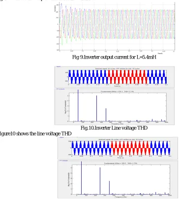
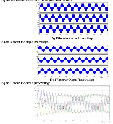
Figure 8 shows the output phase voltage. Figure 9 shows the output current for L=5.4mH.
Fig 9.Inverter output current for L=5.4mH
Fig.10.Inverter Line voltage THD Figure10 shows the line voltage THD
Fig.11.Inverter Phase voltage THD
In the figure 11,it shows the phase voltage THD for diode clamped MLI
In the figure 12,it shows the output current THD for diode clamped MLI.
B.THREE LEVEL MODULAR MULTILEVEL INVERTER
In fig 13 it shows the simulink model of modular multilevel converter.
Fig.13.Modular multilevel converter Simulink Model
Fig.14.Threelevel Modular multilevel converter Simulink model
Figure 14 shows three level modular multi level converter simulink model.
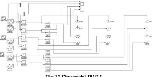
Figure15 shows the SPWM for modular multilevel converter
Fig.16.Inverter Output Line voltage Figure 16 shows the output line voltage.
Fig.17.Inverter Output Phase voltage Figure 17 shows the output phase voltage.
Fig.18.Inverter Output Current for L=5.4mH
Figure 18 shows the output current for L=5.4mH,
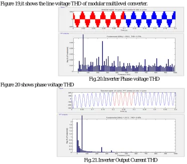
Figure 19,it shows the line voltage THD of modular multilevel converter.
Fig.20.Inverter Phase voltage THD Figure 20 shows phase voltage THD
Fig.21.Inverter Output Current THD
Figure 21 shows the output current THD for three level modular multilevel converter.
Table I shows the comparison of output voltage and current THDs of the two converter topologies. From the table given below it is clear that the total harmonic distortion decreases when moving from diode clamped or neutral pointclamped multilevel inverter to modular multilevel converter.That is THD level is in the order that diode clamped multilevel inverter is greater than modular multilevel converter(MMC).
Table I
Comparison of the current and voltage THDs of various converter topologies
Sl no
Topology Voltage THD(%) Current
THD(%) Line
voltage
Phase voltage
1
Three level diode clamped
Multilevel inverter
5.71 5.72 0.54
2
Three level modular multilevel converter
VI.CONCLUSION
The simulation of three level diode clamped and modular multilevel converters was carried out using sinusoidal pulse width modulation (SPWM).It has shown that there is a decrease in THD when moving from the diode clamped to the modular MLIs. This paper briefly explains the theory of sinusoidal pulse width modulation for both the converters. The performance of converters was analysed using MATLAB/SIMULINK for Rand RL loads and it confirms the performance of modular multilevel converter over diode clamped multilevel inverter.
REFERENCES
[1] Tolbert. L. M and Pend. F. Z, “Multilevel Converter as a Utility Interface for Renewable Energy Systems,” IEEE Power Engineering
Society Meeting, Vol. 2, pp. 1271-1274,2000.
[2] JoseRodriguez, Leopoldo.G.Franquelo,SamirKouro,Jose.I.Leon,Ramon.C.Portil“Multilevel Converters an Enabling Technology for High
power Applications,” IEEE Trans. Ind. Applicat., vol. 97, no. 11, pp. 1786-1816,Nov 2009.
[3] Bose BK. “Power electronics—an emerging technology”. IEEE Transactions on Industrial Electronics, vol.36, no.3, pp. 403–12, August
1989.
[4] P.K.Chaturvedi, S. Jain, Pramod Agrawal “ Modeling , Simulation and, Analysis of Three level Neutral Point Clamped inverter using
mat lab/ Simulink/Power System Blockst”
[5] G.Bhuvaneshwari and Nagaraju “ Multilevel inverters – a comparative study” vol .51 No.2 March – April 2005.
[6] A. Nabae, I. Takahashi, and H. Akagi, “A new neutral- point clamped PWM inverter,” IEEE Trans. Ind. Applicant. Vol. IA-17, pp. 518–
523,Sept. /Oct. 1981.
[7] J. Rodriguez, J. S. Lai, and F. Z. Peng, “Multilevel inverters: A survey of topologies, controls and applications,” IEEE Transactions of
Industrial Electronics, vol.49, no. 4, pp. 724-738, Aug. 2002
[8] B. Urmila, D. Subbarayudu, “Multilevel inverters: A comparative study of pulse width modulation techniques,” International Journal of
Scientific and Engineering Research, vol. 1, issue 3, pp. 1-5, Dec. 2010.
[9] J. Rodriguez, S. Bernet, B. Wu, J. O. Pontt, and S. Kouro, “Multilevel voltage source converter topologies for industrial medium-voltage
drives,” IEEE Transactions on Industrial Electronics, vol. 54, no.6, pp. 2930-2942, Dec. 2007.
[10] Kalle Ilves,Antonios Antonopoulost, Staffan Norrga, Hans-Peter Nee “A New Modulation Method for the Modular Multilevel Converter