260 | P a g e
A New Modified Redundant Binary Multplier Using
Re-dundant Binary Logic
Sowmya Vemula
1, Mahesh Jangam
2 1M.Tech (DSCE),
2Assistant Professor (ECE), Sri Visvesvaraya Institute of Technology &
Science, Chowderpally, Devarkadra, Mahabubnagar
ABSTRACT
A redundant binary (RB) illustration would be utilized when devising elevated presentation multipliers due to its elevated modularity and carry-free summation. The usual RB multiplier needs other RB partial product (RBPP) row, since an error-correcting word (ECW) is produced by both the radix-4 Modified Booth encoding (MBE) and the RB encoding. This sustains in an extra RBPP accumulation part for the MBE multiplier. In this thesis, a novel RB modified partial product generator (RBMPPG) is projected; it removes the additional ECW and thus, it keeps one RBPP accumulation part. As a result, the projected RBMPPG produces less partial product rows than an usual RB MBE multiplier. Simulation outcomes illustrate that the projected RBMPPG supported struc-tures notably progress the area and power utilization while the word length of every operand in the multiplier is as a minimum 32 bits; these reductions over earlier NB multiplier designs sustain in a modest delay increase (approximately 5 percent). The power-delay product would be decreased utilizing the proposed RB multipliers while evaluated with usual RB multipliers. The proposed modified partial product generator is synthesized ex-ploiting XILINX ISE 14.5 simulation tool.
Keywords-
Redundant binary, modified booth encoding, RB partial product generator
I.
INTRODUCTION
Digital multipliers are extensively used in arithmetic units of microprocessors, multimedia and digital signal
processors. Many algorithms and structures have been projected to design eminent-speed and low-power
multip-liers. A normal binary (NB) multiplication by digital systems comprises three stages. Partial products are
pre-pared in the initial stage; all partial products are contained by a partial product reduction tree till two partial
product rows reside in the subsequent stage. The two partial product rows are summed by a fast carry
propaga-tion adder in the next stage. There are two techniques have been used to complete the subsequent stage for the
partial product reduction. A first technique uses four-two compressors, whereas a subsequent technique exploits
redundant binary (RB) numbers. Both methods permit the partial product reduction tree to be decreased at a rate
of 2:1.
The signed-digit arithmetic has been operated using proposed redundant binary number representation; the RB
number has the facility to be characterized in unusual methods. Fast multipliers would be peformed utilizing
261 | P a g e
achieved from two adjoining NB partial product rows by complementing one of the pair rows; an N-bit usual
RB MBE (CRBBE-2) multiplier needs [N/4] RBPP rows. An additional error-correcting word (ECW) is also
needed by together the RB and the Booth encoding; as a result, the amount of RBPP accumulation parts
(NRBPPAS) needed by a power-of-two word-length (i.e., 2n-bit) multiplier is specified by:
….(1)
If the additional ECW would be eliminated, an RBPP accumulation part is kept, thus effecting in developments
of difficulty and critical path delay for a RB multiplier. For instance, an usual 32-bit RB multiplier has four
RBPP accumulation parts; if the ECW is eliminated, then the amount of RBPP accumulation parts is diminished
to 3, i.e., the step calculation is shrinked by 25 percent. Reminder that the difficulty of additional ECW does not
survive in standard significand size (i.e., 24x24-bit and 54x54-bit) RB multipliers as utilized in floating
point-arithmetic units.
This thesis centers on the RBPP generator for intending a 2n-bit RB multiplier through less partial product rows
by removing the superfluous ECW. A novel RB modified partial product generator supported on MBE
(RBMPPG-2) is suggested. In the projected RBMPPG-2, the ECW of every row is stimulated to its
subsequent-ly neighbor row. In addition, the superfluous ECW produced by the preceding partial product row is joined
through both the two most significant bits (MSBs) of the initial partial product row and the two least significant
bits (LSBs) of the preceding partial product row by logic generalization. Therefore, the proposed technique
de-creases the amount of RBPP rows from N/4+1 to N/4, i.e., a RBPP accumulation part is accumulated. The
pro-posed method is applied to 8x8-, 16x16-, 32x32-, and 64x64-bit RB multiplier designs; the designs are
synthe-sized. The projected schemes reach considerable diminutions in area and power utilization evaluated through
presented multipliers while the word length of each of the operands is as a minimum 32 bits. While a reserved
raise in delay is run into (fairly accurately 5 percent), the power-delay product (PDP) at word lengths of as a
minimum 32 bits proves that the projected schemes are the best also by this figure of merit.
This thesis is arranged as follows. Section 2 discusses radix-4 Booth encoding. The structure of the usual RBPP
generator is also explained. Section 3 shows the proposed RBMPPG. This section also represents the acceptance
of the projected RBMPPG into different word-length RB multipliers. The conclusion is given in Section 5.
II. REVIEW OF BOOTH ENCODING AND RB PARTIAL PRODUCT GENERATOR
2.1 Radix-4 Booth Encoding
Booth encoding has been proposed to assist the multiplication of two‟s complement binary numbers. It was
changed as modified Booth encoding or radix-4 Booth encoding. The MBE scheme is reviewed in Table 1,
where A = aN-1aN-2 . . . a2 a1a0 situates for the multiplicand, and B = bN-1bN-2 . . . b2 b1b0 situates for the
262 | P a g e
neighboring collections excluding the initial multiplier bits collection in which it is {b1, b0, 0}. Each collection
is decoded by choosing the partial product illustrated in Table 1, where 2A specifies double the multiplicand,
which would be achieved by left shifting. Negation function is completed by complemening each bit of A and
adding „1‟ (described as correction bit) to the LSB. Techniques have been introduced to explain the trouble of
correction bits for NB radix-4 Booth encoding (NBBE-2) multipliers. Alternatively, this problem has not been
solved for RB MBE multipliers.
Table 1: MBE Scheme
2.2 RB Partial Product Generator
As two bits are utilized to represent one RB digit, then a RBPP is produced from two NB partial products. The
summation of two N-bit NB partial products X and Y using two‟s complement illustration can be stated as
fol-lows:
….(2)
where is the inverse of Y, and the similar convention is used in the remaining of the paper. The composite
number (X, )can be took as a RB number. The RBPP is produced by reversing one of the two NB partial
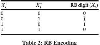
products and adding -1 to the LSB. Each RB digit Xi belongs to the set{ , 0, 1}; this is coded by two bits as the
pair (Xi- ,Xi+ ). Note that = -1. RB numbers can be coded in several ways. Table 2 represents one specific RB
encoding , where the RB digit is reached by performing Xi+- Xi- .
Table 2: RB Encoding
Both MBE and RB coding schemes establish errors and two correction terms are needed: 1) when the NB
num-ber is converted to a RB format, -1 must be appended to the LSB of the RB numnum-ber; 2) when the multiplicand is
263 | P a g e
Fig. 1. Conventional RBPP architecture for an 8-bit MBE multiplier
must be appended to the LSB of the partial product. A solitary ECW would recompense faults from both the
RB encoding and the radix-4 Booth recoding. The conventional partial product architecture of an 8-bit MBE
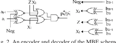
multiplier is illustrated in Fig. 1, where b_p denotes the bit position, p+ij or p-ij is produced by using an encoder
and decoder (Fig. 2) . An N-bit CRBBE-2 multiplier comprises N=4 RBPP rows and one ECW; the ECW takes
the form as follows:
….(3)
where i denotes the ith row of the RBPPs, Ei2ϵ{0,1} and Fi0ϵ{0, }. In Fi0, a-1 correction term is always
needed by RB coding. If Fi0 too corrects the errors from the MBE recoding, then the correction term cancels out
to 0. That is to say that if the multiplicand digit is inverted and added to 1, then Fi0 is 0, otherwise Fi0 is -1. The
error-correcting digit Ei2 is determined only by the Booth encoding:
….(4)
As illustrated in Fig. 1 the first RBPP row, i.e. PP1, contains of the initial partial product row PP+1 and the
second partial product row PP-1 i.e., PP+1 = p+19p+18 . . . p+10and PP-1=p-17p-16 . . . p-10, where, p+19 and p+18 are the
sign extension bits, so
….(5)
….(6)
According to Eq. (2), the sign extension bit p+29 is also the inverse of p +
28. The p
-17 in PP
-1 and the p
-27 in PP
-2 are
also reversed as and . Eq. (5) and Eq. (6) are additional utilized in the subsequently division when
present-ing the proposed modified RBPP generator.
Fig. 2. An encoder and decoder of the MBE scheme
For a 2n-bit CRBBE-2 multiplier, one extra RBPP accumulation part is needed due to the ECW. For a 64-bit RB
multiplier, there are five RBPP accumulation parts; as a result, the number of RBPP accumulation parts can be
decreased by 20 percent when removing the ECW in a 64-bit RB multiplier, which develops both the
264 | P a g e
III.
PROPOSED RB PARTIAL PRODUCT GENERATOR
In this section, a novel RB modified partial product generator supported on MBE (RBMPPG-2) is explained; in
this design, ECW is detached by including it into both the two MSBs of the primary partial product row (PP+1 )
and the two LSBs of the preceding partial product row (PP-(N/4)).
Fig. 3. (a) The first new 2 architecture for an 8-bit MBE multiplier; (b) the further revised
RBMPPG-2 architecture by replacing E22 and F20 with E2, , and; (c) the final proposed RBMPPG-2 architecture by
totally eliminating ECW2 and further combing E2 into Q+19, Q+18, Q-21, and Q-20
3.1 Proposed RBMPPG_2
Fig. 3 shows the projected RBMPPG-2 scheme for an 8x8-bit multiplier. It is different from the scheme in Fig.
1, where all the error-correcting terms are in the last row. ECW1 is produced by PP1 and expressed as
ECW1 = 0 E12 0 F10….(7)
The ECW2 generated by PP2 (also defined as an extra ECW) is
left as the last row and it is expressed as:
ECW2 = 0 E22 0 F20….(8)
To remove a RBPP accumulation part, ECW2 needs to be incorporated into PP1 and PP2. As explained in
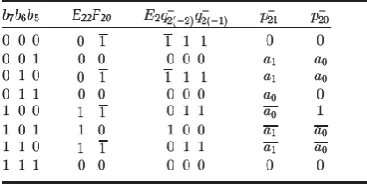
Sec-tion 2.2 for Fi0 and as per Table 1, F 20 is find out by b5, b4, b3 as follows:
265 | P a g e
Table 3: Truth Table of E2, q-2(-2) , q-2(-1) and p-21, p-20As per Table 1, when b5b4b3 = 111, -0 = 0 can be utilized. Therefore, F20 can be stated as follows:
….(10)
By setting PP+2 to all ones and adding +1 to the LSB of the partial product, F20 can then be determined only by
b5 as follows:
….(11)
A modified radix-4 Booth encoding and a decoding circuit for the partial product PP+2 are suggestd here (Fig.
4); an extra threeinput OR gate is then appended to the scheme of (Fig. 2). The three inputs of the additional
OR gate are and . When b5 b4 b3 = 111, it is clear that = 000, p+2i = 1, and PP+2 is set to all ones.
So, E22 and F20 in ECW2 are now find out by b7b6b5 without b4, b3. Although the complexity is slightly boosted
evaluated with the previous design (Fig. 2), the delay stage remains the same.
In this work, Q+19, Q+18, Q-21, and Q-20 are used to represent the modified partial products (i.e., replacing p+19;
p+18, p-21 and p-20). q-2(-2), and q-2(-1) are used to represent the additional partial products that are find out by F20.
As -1 can be coded as 11 in RB format, E22 and F20 can be represented by E2, q-2(-2), q-2(-1), (Fig. 3b) as
fol-lows:
….(12)
….(13)
As per Eq. (11) and Eq. (13), q-2(-2), and q-2(-1) would too be stated as follows:
….(14)
This is further discussed by the truth table of E22, F20 and E2, q
-2(-2) , q
-2(-1) (Table 3). Now ECW2 only includes
E2 and E2ϵ {0,1, }; E2 can be integrated into the modified partial products Q+19, Q+18, Q+21 and Q-20 by
replac-ing p+19, p+18 and p-21 , p-20 in the shortest path Fig. 3c. From the truth table, E2 can be find out by b7b6b5 as
fol-lows:
266 | P a g e
Fig. 4. The modified radix-4 Booth encoding and decoding scheme for PP+2Table 4 The Truth Table of Q+19, Q+18, Q-21, Q-20
So the following three cases can be distinguished: 1) When E2 = 0, Q +
19, Q +
18, Q
-21 and Q
-20 remain unchanged
as: Q+19 = p+19, Q+18 = p+18, Q-21 = p-21 and Q-20 = p-20. 2) When E2 = 1, a 1 is added to p+19 ,p+18 ,p-21 ,p-20. 3)
When E2 = -1, a 1 is subtracted from p+19p+18p-21p-20.
The relationships between Q+19, Q+18, Q-21, Q-20 and p+19, p+18, p-21, p-20 are reviewed in Table 4. As the two
MSBs of PP+1 i.e., p+19 and p+18 take complementary values as shown in Eq. (5), the operations of adding or
sub-tracting a 1 will never sustain in an overflow. Therefore, as per Eq. (15) and Table 4, the logic functions of Q+19,
Q+18, Q-21, and Q-20 would be stated as follows:
….(16)
….(17)
….(18)
….(19)
The delay of the RBMPPG-2 can be further decreased by generating Q+19, Q+18, Q-21, Q-20 directly from the
mul-tiplicand A and the multiplier B. The associations among p+19, p+18 and A, B have been explained in Section 2.2
as Eq. (5) and Eq. (6). The relationships between p-21, p-20 and A, B are also shown in Table 3 concurrencing to
the MBE scheme. Therefore, Q+19, Q+18, Q-21, and Q-20 would be stated as follows by replacing p+19, p+18, p-21,
and p-20 with the multiplicand bits (ai) and the multiplier bits (bi) after simplification:
….(20)
267 | P a g e
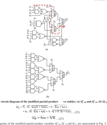
Fig. 5. The circuit diagram of the modified partial product va riables: (a) Q+18 and Q+19, (b) Q-21.….(22)
….(23)
The circuit diagrams of the modified partial product variables Q+18, Q+19 and Q-21 are represented in Fig. 5. It is
clear that Q+18 has the longest delay path. It is well known that the inverter, the 2-input NAND gate and the
transmission gate (TG) are faster than other gates. So, this is popular to use TGs when designing the
multiplex-er. As illustrated in Fig. 5a, the critical path delay (the dash line) contains of a 1-stage AND-OR-Inverter gate, a
one-stage inverter, and two-stage TGs. Therefore, RBMPPG-2 just boosts the TG delay by one-stage evaluated
with the MBE partial product of Fig. 2.
The above explanation is only an example; the above method would be concerned to intend any 2n-bit RB
mul-tipliers. It eliminates the superfluous ECWN/4 and saves one RBPP accumulation stage, i.e., three XOR gate
de-lays, whereas only a little amplifying the delay of the partial product generation stage. In common, an N-bit RB
multiplier has N=4 RBPP rows utilizing the proposed RBMPPG-2. The partial product variables p+1(N+1), p+1N,
p-(N/4)1 and p-(N/4)0 can be reinstated by Q+1 (N+1), Q+1 N, Q-(N/4)1, and Q-(N/4)0. The radix-4 Booth decoding of a
PPR (PP+N/4) needs additional three-input OR gates (Fig. 4). Therefore, the superfluous ECWN/4 is removed by
the transformation of four partial product variables Q+1(N+1), Q+1N, Q-(N/4)1, Q-(N/4)0 and one partial product row is
268 | P a g e
Fig. 6. The block diagram of a 32-bit RB multiplier using the proposed RBMPPG-2
3.2 Design of RBMPPG-2-Based High-Speed RB Multipliers
The projected RBMPPG-2 can be useful to any 2n-bit RB multipliers through a diminution of a RBPP
accumula-tion part evaluated with usual designs. Even though the delay of RMPPG-2 boosts by one-stage of TG delay, the
delay of one RBPP accumulation part is mainly bigger than a one-stage TG delay. Therefore, the delay of the
entire multiplier is decreased. The progressd complexity, delay and power utilization are very striking for the
proposed design.
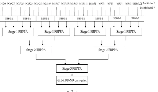
The multiplier includes of the projected RBMPPG-2, three RBPP accumulation stages, and one RB-NB
conver-ter. A 32-bit RB multiplier developing the projected RBPP originator is represented in Fig. 6. Eight RBBE-2
blocks make the RBPP (p+i, p-i ); they are added up by the RBPP reduction tree that has three RBPP
accumula-tion stages. Each RBPP accumulaaccumula-tion obstruct includes RB full adders (RBFAs) and half adders (RBHAs). The
64-bit RB-NB converter translates the last accumulation outcomes into the NB illustration, which utilizes a
hy-brid parallel-prefix/carry select adder (as solitary of the mainly capable fast parallel adder designs).
There are four steps in an usual 32-bit RB MBE multiplier architecture; however, by utilizing the projected
RBMPPG-2,the amount of RBPP accumulation parts is diminished from 4 to 3 (i.e., a 25 percent reduction).
These are important savings in delay, area as well as power utilization. The developments in delay, area and
power consumption are further demonstrated in the subsequently segment by simulation.
For a 64-bit multiplier, the projected scheme has four RBPP accumulation steps; it decreases the partial product
accumulation delay time by 20 percent evaluated through CRBBE-2 multipliers. Although both the projected
scheme and RBBE-4 have the same amount of RBPP accumulation stages, RBBE-4 is more complex,because it
utilizes radix-16 Booth encoding.
IV. SYNTHESIS AND SIMULATION RESULTS
The projected RB multiplier employing the projected RBMPPG-2 is designed with the XILINX ISE 14.5
269 | P a g e
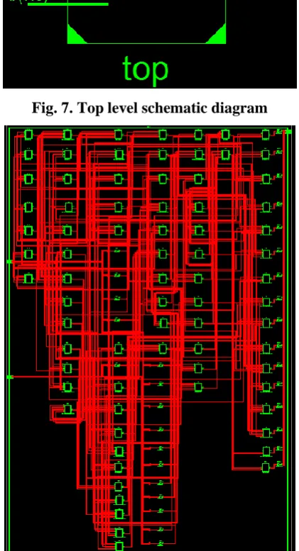
Fig. 7. Top level schematic diagram
Fig. 8. Internal architectures of RTL diagram
270 | P a g e
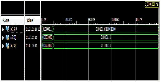
Fig. 10. Simulation result
V. CONCLUSION
In this thesis, a novel modified RBPP generator has been proposed; this design eliminates the extra ECW that is
introduced by previous designs. Therefore, a RBPP accumulation part is kept due to the elimination of ECW.
Simulation results have shown that the performance of RB MBE multipliers utilizing the projected RBMPPG-2
is improved significantly in terms of delay and area. Synthesis of proposed system done by the Verilog HDL
synthesized in Xilinx ISE 14.5. The projected schemes complete main diminutions in area and power utilization
when the word length is as a minimum 32 bits. The projected RBPP generation method is a very useful
tech-nique when designing area and PDP efficient power-of-two RB MBE multipliers.
VI. FUTURE SCOPE
In this proposed paper, we modify the multiplier by boosting the amount of input to the multiplier. In our
modi-fication these inputs are in 64 bits and the output in 128 bits.
REFERENCES
[1] A. Avizienis, “Signed-digit number representations for fast parallel arithmetic,” IRE Trans. Electron.
Comput., vol. EC-10, pp. 389–400, 1961.
[2] N. Takagi, H. Yasuura, and S. Yajima, “High-speed VLSI multiplication algorithm with a redundant
bi-nary addition tree,” IEEE Trans. Comput., vol. C-34, no. 9, pp. 789–796, Sep. 1985.
[3] Y. Harata, Y. Nakamura, H. Nagase, M. Takigawa, and N. Takagi, “A high speed multiplier using a
re-dundant binary adder tree,” IEEE J. Solid-State Circuits, vol. SC-22, no. 1, pp. 28–34, Feb. 1987.
[4] H. Edamatsu, T. Taniguchi, T. Nishiyama, and S. Kuninobu, “A 33 MFLOPS floating point processor
using redundant binary representation,” in Proc. IEEE Int. Solid-State Circuits Conf., 1988, pp. 152–153.
[5] H. Makino, Y. Nakase, and H. Shinohara, “A 8.8-ns 54x54-bit multiplier using new redundant binary
architecture,” in Proc. Int. Conf. Comput. Des., 1993, pp. 202–205.
[6] H. Makino, Y. Nakase, H. Suzuki, H. Morinaka, H. Shinohara, and K. Makino, “An 8.8-ns 54_54-bit
multiplier with high speed redundant binary architecture,” IEEE J. Solid-State Circuits, vol. 31, no. 6, pp.
773–783, Jun. 1996.
[7] Y. Kim, B. Song, J. Grosspietsch, and S. Gillig, “A carry-free 54b_54b multiplier using equivalent bit
271 | P a g e
[10] W. Yeh and C. Jen, “High-speed booth encoded parallel multiplier design,” IEEE Trans. Comput., vol.
49, no. 7, pp. 692–701, Jul. 2000.
AUTHOR DETAILS
SOWMYA VEMULA, pursuing M.Tech (DSCE) from Sri Visvesvaraya Institute Of
Technology & Science, Chowderpally (Vill), Devarkadra (Mdl), Mahabubnagar (Dist),
TS, INDIA.
MAHESH JANGAM, working as Assistant professor (ECE) from Sri Visvesvaraya
Insti-tute Of Technology & Science, Chowderpally (Vill), Devarkadra (Mdl), Mahabubnagar