Design and Implementation of AMBA based
AXI 4 Slave Interface
Mahesh Pai N
1, H Sudha
2, Lakshmikantha HN
3Final Year M.Tech (VLSI Design & Embedded Systems) Student, Department of E&CE, Bangalore Institute of
Technology, Bangalore, Karnataka, India1
Associate Professor, Department of E&CE, Bangalore Institute of Technology, Bangalore, Karnataka, India2
Project Manager, Mindtree Ltd, Bangalore, Karnataka, India3
ABSTRACT: The important aspect of a SoC is not only which components or blocks it houses, but also how they interconnect. AMBA is a solution for the blocks to interface with each other. These protocols are today the de facto standard for 32-bit embedded processors because they are well documented and can be used without royalties. The AMBA AXI 4 protocol supports high-performance, high-frequency system designs. It is suitable for high-bandwidth and low-latency designs and provides high-frequency operation without using complex bridges. It provides flexibility in the implementation of interconnect architectures and is backward-compatible with existing AHB and APB interfaces. This Project is aimed at the Design of the AXI4 Slave Interface and implementation using Verilog RTL coding. This slave interface can be used to connect different peripherals into AMBA based processors without using bridge. The developed slave interface can also be used to connect different peripherals like SPI, I2C, UART etc., into non AMBA based processors by developing wrapper around AXI4 slave interface.
KEYWORDS: Advanced Microcontroller Bus Architecture (AMBA), Advanced Extensible Interface (AXI).
I. INTRODUCTION
AXI stands for Advanced Extensible Interface. It is a part of the Advanced Microcontroller Bus Architecture (AMBA) developed by ARM (Advanced RISC Machines) company. It is an On-Chip communication protocol. The AMBA AXI protocol supports high-performance, high-frequency system designs.
The AXI protocol is suitable for high-bandwidth and low-latency designs. It provides high-frequency operation without using complex bridge. It meets the interface requirements of a wide range of components. AXI protocol is suitable for memory controllers with high initial access latency. It provides flexibility in the implementation of interconnect architectures. It is backward-compatible with existing AHB and APB interfaces.
AMBA was introduced by ARM in 1996. The first AMBA buses were Advanced System Bus (ASB) and Advanced Peripheral Bus (APB) [1&2]. In its second version, AMBA 2, ARM added AMBA High-performance Bus (AHB) that is a single clock-edge protocol [3-5]. In 2003, ARM introduced the third generation, AMBA 3 [6&7], including AXI to reach even higher performance interconnect and the Advanced Trace Bus (ATB) as part of the CoreSight on-chip debug and trace solution. In 2010 the AMBA 4 specifications were introduced starting with AMBA 4 AXI4, then in 2011 extending system wide coherency with AMBA 4 ACE with a re-designed high-speed transport layer and features designed to reduce congestion [8-10].
Advanced microcontroller bus architecture (AMBA) protocol family provides metric-driven verification of protocol compliance, enabling comprehensive testing of interface intellectual property (IP) blocks and system-on-chip (SoC) designs. The AMBA advanced extensible interface 4 (AXI4) update to AMBA AXI3 includes the following: support for burst lengths up to 256 beats, updated write response requirements, removal of locked transactions and AXI4 also includes information on the interoperability of components. AMBA AXI4 protocol system supports 16 masters and 16 slaves interfacing. The design is implemented using Verilog- HDL [11-13].
III. AXI PROTOCOL SPECIFICATIONS
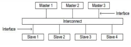
A typical system consists of a number of master and slave devices connected together through the Interconnect. The AXI protocol provides a single interface definition, for the interfaces:
• Between a master and the interconnect • Between a slave and the interconnect • Between a master and a slave.
Figure 1: AXI System Topology
The AXI protocol is burst-based and defines the following independent transaction channels: Read Address Channel, Read Data Channel, Write Address Channel, Write Data Channel and the Write Response Channel.
An address channel carries control information that describes the nature of the data to be transferred. The data is transferred between master and slave using either:
A write data channel to transfer data from the master to the slave. In a write transaction, the slave uses the write response channel to signal the completion of the transfer to the master.
A read data channel to transfer data from the slave to the master.
Figure 2: AXI Channel Architecture
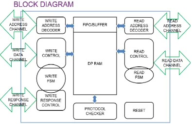
IV. PROPOSED SLAVE ARCHITECTURE
The AXI Slave has been designed and verified using Master-Verification IP. The design for slave has the five bi-directional channels as the Input/ Output. The design is done using the finite state machine approach. The Read/Write controllers are governed by the respective state machines.
Write Control: This block controls the data and the rate at which it is written into the FIFO/DPRAM. Write Response Control: This block controls the response signals that are sent back to the master.
Read Address Decoder: This block decodes the incoming address from the read address channel sent from the master. Read Control: This block controls the data and the rate at which it is read from the FIFO/DPRAM.
Protocol Checker: Constantly checks for the controls signals as to whether they’re in line with the desired protocol. Reset: This block allows for asynchronous assertion and synchronous de-assertion of the global reset signal.
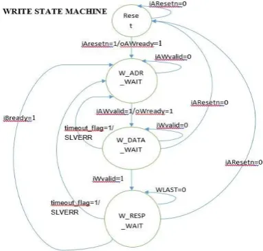
Write FSM: This block governs the blocks 1,2& 3. Figure 4-2 shows the main state diagram of the complete write transaction.
Figure 4: Write Transaction State Machine
The write state machine consists of 4 states that include the reset, address wait, data wait and response wait. The reset state is the initial state. The state machine abandons all other functions and reverts to this state if the reset signal is asserted. In the address wait state, the slave awaits the address and control information from the Master for the write transaction. The data wait state follows the address handshake and continues with the data transfer for write. In the response wait state the slave awaits for the last data and then handshake via the response channel and confirms the data transaction with a response signal.
The read state machine consists of 3 states that include the reset, address wait and the data wait. The reset state is the initial state. The state machine abandons all other functions and reverts to this state if the reset signal is asserted. In the address wait state, the slave awaits the address and control information from the Master for the read transaction. The data wait state follows the address handshake and continues with the data transfer for the read. The read transaction does not involve a separate channel for response hence it provides a response signal for every data transfer instead of the last data transfer over the read data channel itself.
FIFO/DPRAM: This block depicts the types of memory used for the slave. It consists of an asynchronous FIFO and a dual port RAM.
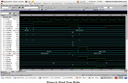
V. SIMULATION RESULTS
The results consists of simulation waveforms that are obtained during verification of the DUT. The waveforms are used to verify the functionality of the Slave. It is found that the DUT is functional and performs intended behaviour of an AXI 4 Slave of the desired functionality.
Figure 6: Fixed Type Write
Figure 7: Fixed Type Read
The above figure shows the fixed type read operation. The data is received from the same address of the slave just as emptying a FIFO.
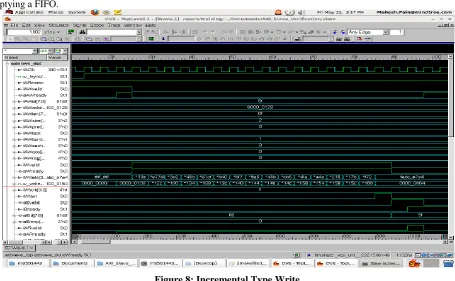
The above figure shows the Incremental (INCR) type write operation. The data is sent as a burst with one given starting address. The slave calculates the subsequent transfer address based on the burst length, size and type. The data is stored accordingly in the memory.
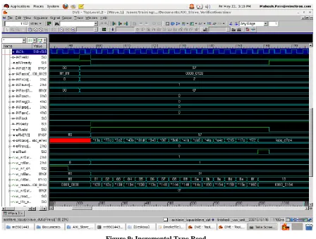
Figure 9: Incremental Type Read
The above figure shows the Incremental (INCR) type read operation. The data is sent as a burst from the slave to the master with one given starting address. The slave calculates the subsequent transfer address based on the burst length, size and type. The data is sent accordingly from the memory to the master.
VI. CONCLUSION AND FUTURE SCOPE
REFERENCES
[1] “AMBA Peripheral Bus Controller Data Sheet” Copyright © 1996 Advanced RISC Machines Ltd (ARM).
[2] Ramagundam, S.; Dept. of Computer Sci., Troy Univ., Montgomery, AL, USA ; Das, S.R. ; Morton, S. ; Biswas, S.N. , “Design and implementation of high-performance master/slave memory controller with microcontroller bus architecture”, Instrumentation and Measurement Technology Conference (I2MTC) Proceedings, 2014 IEEE International, 12-15 May 2014.
[3] “AMBA™ Specification (Rev 2.0)” 13th May 1999-A, First release, Copyright ARM Limited 1999.
[4] “Soo-Yun Hwang; Dept. of Comput. Eng., ChungNam Nat. Univ., Taejon, South Korea; Kyoung-Sun Jhang “An improved implementation method of AHB Bus Matrix”, SOC Conference, 2005. Proceedings. IEEE International, 25-28 Sept. 2005
[5] Hu Yueli; Key Lab. of Adv. Display & Syst. Application., Shanghai Univ., Shanghai, China ; Yang Ben “Building an AMBA AHB Compliant Memory Controller”, Measuring Technology and Mechatronics Automation (ICMTMA), 2011 Third International Conference, 6-7 Jan. 2011.
[6] “AMBA AXI Specification (AR500-DA-10008)” 16 June, 2003-A, First release, Copyright ARM Limited 2003
[7] Paunikar, A.; Sch. of Electron. Eng., VIT Univ., Vellore, India ; Gavankar, R.; Umarikar, N. ; Sivasankaran, K. , “Design and implementation of area efficient, low power AMBA 3-APB Bridge for SoC” , Green Computing Communication and Electrical Engineering (ICGCCEE), 2014 International Conference, 6-8 March 2014
[8] “AMBA AXI 4 and ACE Protocol Specification” 28 October 2011 D Non-Confidential First release of AMBA AXI 4 and ACE Protocol Specification.
[9] Xu Yang ; Harbin Inst. of Technol., Harbin ; Zhang Qing-li ; Fu Fang-fa ; Yu Ming-yan, “NISAR: An AXI compliant on-chip NI architecture offering transaction reordering processing” ASIC, 2007. ASICON '07. 7th International Conference, 22-25 Oct. 2007. [10] Manjula, R.B. ; Manvi, S.S. ; Kaunds, P. “Data transactions on system-on-chip bus using AXI4 protocol” Recent Advancements in
Electrical, Electronics and Control Engineering (ICONRAEeCE), 2011 International Conference, 15-17 Dec. 2011.
[11] “Verilog-A Language Reference Manual Analog Extensions to Verilog HDL”, Version 1.0, Open Verilog International August 1, 1996 [12] “Verilog-AMS Language Reference Manual”, Release 2.3.1, Accellera Systems Initiative , 06-2009