A High-Performance Modified AXI Master Slave
on-Chip Bus Design and Verification
Nandi Vardhan1, Nithish Gangula2, Jagniwas kumar3, Jayasurya Uppala4, B. Eshwar5
1,2,3,4
Students, 5Asst. Professor, Department of Electronics and Communication Engineering, Lords Institute of Engineering and Technology, Hyderabad, Telangana, India.
Abstract: Complex VLSI IC design has been revolutionized by the widespread adoption of the SoC paradigm. The benefits of the SoC approaches are numerous, including improvements in system performance, cost, size, power dissipation, and design turnaround time. As the level of chip integration continuous to advances at a fast pace, the desire for efficient interconnects rapidly increase. Currently on-chip interconnections networks are mostly implemented using traditional interconnects like buses. So, in general the performance of the SoC design heavily depends upon the efficiency of its bus structure.
This project proposes a high-performance system-on-chip bus protocol termed the AXI master-slave bus. This MSBUS is composed of a control bus (MBUS) and a data bus (SBUS). Considering the inevitable tradeoff among area, throughput and energy efficiency, the control bus is developed as a low-cost and low-power bus, and the data bus is created as a high-throughput full-duplex bus with the future of block data transfer. This bus protocol uses shared bus layers (channels), which reduce the number of wires required. That increases wire usage efficiency and simplifies the hardware interconnections as well as minimal power consumption and reduced interface complexity.
Keywords: System on-chip (SoC), wire efficiency, Xilinx, FPGA, Channel Reduction.
I. INTRODUCTION
application-specific models including Wi-Fi Mac, Bluetooth 4.0 controller, USB 2.0 host controller and Security module are the slaves of MBUS and the masters of SBUS. They are controlled by the microprocessor through MBUS and access the only slave memory through SBUS.
II. LITERATURE SURVEY
The paper titled “An AMBA AHB-based reconfigurable SoC architecture using multiplicity of dedicated flyby DMA blocks” proposed a System-on-Chip (SoC) architecture for reconfigurable applications based on the AMBA High-Speed Bus (AHB). The architecture features multiple low-area fly by DMA blocks for transferring configuration data. Furthermore, the architecture eliminates the use of energy consuming instructions used in comparable commercial reconfigurable SoCs. The flyby DMA blocks achieve a reduction of up to 98% in the number of gates found in general-purpose DMA controllers. The DMA blocks also achieve the flyby throughput which halves the number of clock cycles used in conventional DMA for data transfer.
Flyby DMAC and dedicated channels DMAC adopt non- buffer data transmission mode, and the advantage of this mode is improvement of the efficiency of data transfer, but when rapid data blocks transfer proceed in equipments which are on the same group of bus or data movement in the same port that is common in audio and video codec application, this mode is no longer applicable. Because non-buffer DMAC cannot achieve write operation after reading in single-cycle.
The paper titled “Design and Implementation of an Advanced DMA Controller on AMBA-Based SoC” proposed a design and implementation of an AMBA based advanced DMA controller architecture which lies in between AHB bus and APB bus, with APB Bridge function, that is, DMAC controls directly data, address and control signals on APB bus. So it could achieve AHB operation and APB operation run in parallel. And data transfer mode can be buffer and non-buffer mode according to practical application by setting control register. AHB Master module asserts bus request signal to get access to the AHB according to parameter set, and completes data transfer between AHB and FIFO. APB Master module asserts bus request signal to gain the control of APB after arbitration with APB Bridge, and completes data transfer between APB and FIFO. However, the additional area of the separated address channels is the penalty and wire usage efficiency of these buses is less.
III. PROPOSED SYSTEM
The paper titled “A High-Performance Modified AXI Master Slave On-Chip Bus Design and Verification” Proposed a high-performance system-on-chip bus protocol. MSBUS is composed of a control bus (MBUS) and a data bus (SBUS). Considering the inevitable tradeoff among area, throughput and energy efficiency, the control bus is developed as a low-cost and low-power bus, and the data bus is created as a high-throughput full-duplex bus with the feature of block data transfer. This bus protocol uses shared bus layers, which reduces the number of wires (channels) required. That increases wire usage efficiency and simplifies the hardware interconnections.
Thus the above proposed design overcomes with the following advantages over former two designs:
A. High wire usage efficiency,
B. Less hardware interconnections,
C. Minimal power consumption,
D. Reduced interface complexity,
E. Low cost,
F. Block data transfer.
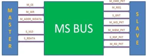
IV. BLOCK DAIGRAM
[image:2.612.185.427.627.719.2]MSBUS is composed of a control bus (MBUS) and a data bus (SBUS). MBUS stands for master bus with a single master—the microprocessor and SBUS stands for slave bus with a single slave— the memory controller.
Let the prefixes “M_” and “S_” are from the master and the slave signals, respectively. Notice that “M_ADDR_WDATA” is created as a shared bus with write address, read address, and write data information. A pair of handshake signals, “M_REQ” and “S_GNT”, ensures that there is only one master occupying the write or read channel at the same time. The other SBUS signals are categorized into five packets.
A. Command (M_CMD_PKT[42:0])
B. Write data (M_WD_PKT[31:0]),
C. write data mask (M_WBM_PKT[3:0]),
D. read data (M_RD_PKT[31:0]),
E. Response (S_RSP_PKT[1:0]).
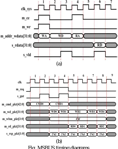
V. TIMING DIAGRAMS
MBUS defines the SINGLE transfer mode with at least one-cycle command and one-cycle data. It is optimized for minimal power consumption and reduced interface complexity. As shown in Fig. 5.1(a), let the prefixes “M_” and “S_” are from the master and the slave signals, respectively hereafter. Notice that “M_ADDR_WDATA” is created as a shared bus with write address, read address, and write data information. It increases wire usage efficiency and simplifies the hardware interconnection. Second, MBUS does not require arbitration due to the single-master structure, so the command stage takes only one master cycle. Third, the valid signal (S_VLD) used to acknowledge the request is necessary to synchronize signals crossing between master and slave clock domain and avoid command FIFO overflows. Finally, a response delay timer is defined in the MBUS protocol to detect command errors. If the current response is a timeout, the command is indicated as “error” and must be “retried” or “discarded” by the master.
(a)
[image:3.612.190.422.328.621.2](b)
Fig. MSBUS timing diagrams. (a) MBUS protocol. (b) SBUS protocol.
VI. FLOWCHART
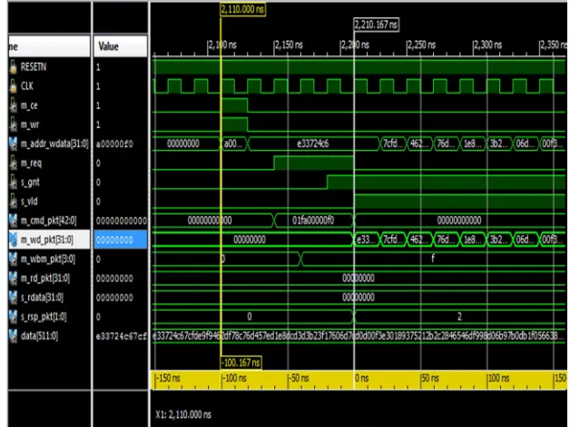
VII. SIMULATION RESULTS A. Write Transaction
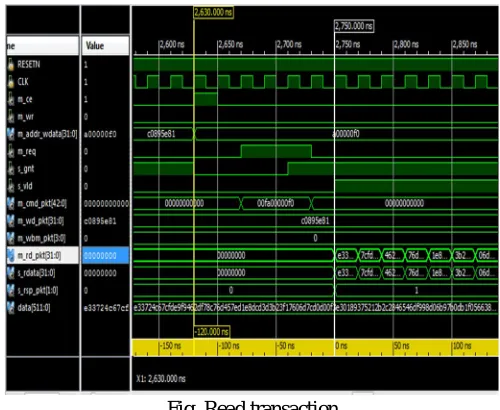
B. Read Transactions
Fig. Read transaction
VIII. CONCLUSION
This paper proposed a high-performance bus with shared bus layers (channels), reduced interface complexity, minimal power consumption, and high throughput. This bus protocol uses shared bus layers, which reduces the number of bus layers required. These reduced number of bus layers, increases wire usage efficiency and simplifies the hardware interconnections as well as minimal power consumption and reduced interface complexity.
In this paper, VERILOG HDL programming has been used in the implementation of MSBUS.
And the Programming tool used for the implementation is Xilinx ISE-13.1. The design is implemented using FPGA Spartan 3-E. The single-processor and multiclient bus structure of MSBUS reduces resource utilization and energy consumption and limits the complexity of circuits. Therefore, the MSBUS protocol is very desirable for small-scale embedded systems with requirements of a low-cost interface and high-energy efficiency.
IX. FUTURE SCOPE
The MSBUS design proposed in this paper focused on providing the bus with shared bus layers (channels) which reduced interface complexity, minimal power consumption, and high throughput. However, the MSBUS protocol is designed with a single processor (master) and multiple slaves. A direction for future work involves the creation of multi master with the above features. So that its applications are extended to large-scale embedded systems.
REFERENCES [1] AMBA Specification, Axis, Sunnyvale, CA, USA, 1999.
[2] AMBA AXI Protocol Specification, Axis, Sunnyvale, CA, USA, 2003. [3] Wishbone BUS, Silicore Corp., Corcoran, MN, USA, 2003.
[4] Open Core Protocol Specification, OCP Int. Partnership, Beaverton, OR, USA, 2001. [5] CoreConnect Bus Architecture, IBM, Yorktown Heights, New York, NY, USA, 1999. [6] STBus Interconnect, STMicroelectronics, Geneva, Switzerland, 2004.
[7] R. C. Gonzalez and R. E. Woods, Digital Image Processing, 3rd ed. Englewood Cliffs, NJ, USA: Prentice-Hall, Jun. 2012, pp. 68–99. [8] Wireless LAN Medium Access Control (MAC) and Physical Layer (PHY) Specification, IEEE Standard 802.11-1999, 1999.
[9] Xiaokun Yang and Jean H. Andrian “A High-Performance On-Chip Bus (MSBUS) Design and Verification “, IEEE Transactions on Very Large Scale Integration (VLSI) Systems (Volume:PP , Issue: 99 ) JUN-2014..
[10] K. Sekar, K. Lahiri, A. Raghunathan, and S. Dey, “Dynamically configurable bus topologies for high-performance on-chip communication,” IEEE Trans. Very Large Scale Integr. (VLSI) Syst., vol. 16, no. 10,pp. 1413–1426, Oct. 2008.
[11] S. Kim and S. Ha, “Efficient exploration of bus-based system-on-chip architectures,” IEEE Trans. Very Large Scale Integr. (VLSI) Syst., vol. 14, no. 7, pp. 681–692, Jul. 2006.
[12] P.-C. Hsiu, C.-K. Hsieh, D.-N. Lee, and T.-W. Kuo, “Multilayer bus optimization for real-time embedded systems,” IEEE Trans. Comput., vol. 61, no. 11, pp. 1638–1650, Nov. 2012.
[14] S. Hwang, D. Kang, H. Park, and K. Jhang, “Implementation of a self-motivated arbitration scheme for the multilayer AHB busmatrix,” IEEE Trans. Very Large Scale Integr. (VLSI) Syst., vol. 18, no. 5, pp. 818–830, May 2010.
[15] Y.-S. Cho, E.-J. Choi, and K.-R. Cho, “Modeling and analysis of the system bus latency on the SoC platform,” in Proc. Int. Workshop System-Level Interconnect Predict., New York, NY, USA, Mar. 2006, pp. 67–74.
[16] J. Lee and H.-J. Lee, “Wire optimization for multimedia SoC and SiP designs,” IEEE Trans. Circuits Syst. I, Reg. Papers, vol. 55, no. 8, pp. 2002–2215, Sep. 2008.
[17] J. Lee, H.-J. Lee, and C. Lee, “A phase-based approach for on-chi bus architecture optimization,” Comput. J., vol. 52, no. 6, pp. 626–645, Aug. 2009.
[18] Guoliang Ma* and Ru Re “Design and Implementation of an Advanced DMA Controller on AMBA-Based SoC” IEEE Trans on Very Large Scale Integr. (VLSI) Syst., May.2009.
[19] Adeoye Olugbon I, Saw Khawam I, Tughrul Arslan , Ioannis Nousias ', rain Lindsay “AN AMBA AHB-BASED RECONFIGURABLE SOC ARCHITECTURE USING MULTIPLICITY OF DEDICATED FLYBY DMA BLOCKS” IEEE Trans on Very Large Scale Integr. (VLSI) Syst.,Jun.2008. [20] A. Lakshminarayana, S. Ahuja, and S. Shukla, “High level power estimation models for FPGA,” in Proc. IEEE Comput. Soc. Annu. Symp. VLSI, Jul. 2011, pp.
7–12.
[21] C. Chung and J. Kim, “Broadcast filtering: Snoop energy reduction in shared bus-based low-power MPSoCs,” J. Syst. Archit., vol. 55, no. 3, pp. 196–208, Mar. 2009.
[22] UVM 1.1 Reference Manual, Accellera, Tualatin, OR, USA, Jun. 2011. [23] UVM 1.1 User Guide, Accellera, Tualatin, OR, USA, May 2012.
AUTHOUR’S OUTLINE
1) Mr. Nandi Vardhan is currently pursuing his B.Tech in Electronics and Communication Engineering from Lords Institute of
Engineering and Technology, Himayathsagar, Hyderabad, TS, India. E-mail: [email protected]
2) Mr. Nithish Gangula is currently pursuing his B.Tech in Electronics and Communication Engineering from Lords Institute of
Engineering and Technology, Himayathsagar, Hyderabad, TS, India. E-mail: [email protected]
3) Mr. Jagniwas Kumar is currently pursuing his B.Tech in Electronics and Communication Engineering from Lords Institute of
Engineering and Technology, Himayathsagar, Hyderabad, TS, India. E-mail: [email protected]
4) Mr. Jayasurya Uppala is currently pursuing his B.Tech in Electronics and Communication Engineering from Lords Institute
of Engineering and Technology, Himayathsagar, Hyderabad, TS, India. E-mail: [email protected]
5) Mr. B. Eshwar, completed BE and ME from OU. Has three year experience in teaching. Field of interest is VLSI, Analog electronics, Pulse and Digital circuits. Presently working as Asst. Professor in Department of Electronics and Communication Engineering, Lords Institute of Engineering and Technology, Himayathsagar, Hyderabad, TS, India.