warwick.ac.uk/lib-publications
Original citation:
Holmes, S. N., Newton, P. J., Llandro, J., Mansell, R., Barnes, C. H. W., Morrison, Christopher and Myronov, Maksym. (2016) Spin-splitting in p-type Ge devices. Journal of Applied Physics, 120 (8). 085702.
Permanent WRAP URL:
http://wrap.warwick.ac.uk/81459
Copyright and reuse:
The Warwick Research Archive Portal (WRAP) makes this work by researchers of the University of Warwick available open access under the following conditions. Copyright © and all moral rights to the version of the paper presented here belong to the individual author(s) and/or other copyright owners. To the extent reasonable and practicable the material made available in WRAP has been checked for eligibility before being made available.
Copies of full items can be used for personal research or study, educational, or not-for-profit purposes without prior permission or charge. Provided that the authors, title and full bibliographic details are credited, a hyperlink and/or URL is given for the original metadata page and the content is not changed in any way.
Publisher’s statement:
This article may be downloaded for personal use only. Any other use requires prior permission of the author and AIP Publishing.
The following article appeared in Holmes, S. N., Newton, P. J., Llandro, J., Mansell, R., Barnes, C. H. W., Morrison, Christopher and Myronov, Maksym. (2016) Spin-splitting in p-type Ge devices. Journal of Applied Physics, 120 (8). 085702. and may be found at
http://dx.doi.org/10.1063/1.4961416
A note on versions:
The version presented in WRAP is the published version or, version of record, and may be cited as it appears here.
Spin-splitting in p-type Ge devices
S. N.Holmes,1,a)P. J.Newton,1J.Llandro,1R.Mansell,1C. H. W.Barnes,1C.Morrison,2 and M.Myronov2
1
Cavendish Laboratory, Department of Physics, University of Cambridge, J. J. Thomson Avenue, Cambridge CB3 0HE, United Kingdom
2
Department of Physics, University of Warwick, Coventry CV4 7AL, United Kingdom
(Received 4 May 2016; accepted 7 August 2016; published online 23 August 2016)
Compressively strained Ge quantum well devices have a spin-splitting in applied magnetic field that is entirely consistent with a Zeeman effect in the heavy hole valence band. The spin orientation is determined by the biaxial strain in the quantum well with the relaxed SiGe buffer layers and is quantized in the growth direction perpendicular to the conducting channel. The measured spin-splitting in the resistivity qxx agrees with the predictions of the Zeeman Hamiltonian where the Shubnikov-deHaas effect exhibits a loss ofevenfilling factor minima in the resistivity qxx with hole depletion from a gate field, increasing disorder or increasing temperature. There is no measur-able Rashba spin-orbit coupling irrespective of the structural inversion asymmetry of the confining potential in low p-doped or undoped Ge quantum wells from a density of 61010cm2in deple-tion mode to 1.71011cm2in enhancement.Published by AIP Publishing.
[http://dx.doi.org/10.1063/1.4961416]
I. INTRODUCTION
The present trend in miniaturization of complementary metal-oxide-semiconductor (CMOS) silicon devices1 to shorter gate length and thinner oxide dielectric, following the predictions of Moore’s law, has come at a cost ofreduced per-formance withincreasingpower consumption.2Replacing Si with higher mobility Ge can go some way to alleviating these problems.3However, new device schemes operating on funda-mentally different physical principles to the field effect tran-sistor are needed to achieve higher processing speeds in combination with reduced levels of waste heat. A viable mechanism for this alternative technology to rival CMOS is spin current manipulation in hybrid metal/Ge semiconductor channels.4,5 To utilize such spin currents in a voltage-controllable fashion, the spin-orbit coupling mechanism that leads to electric field tunable spin-splitting needs to be quanti-fied in Ge quantum wells (QWs). This paper addresses this spin-splitting behaviour in applied magnetic fields and is set out in Secs. II–V. In Section II, device fabrication is dis-cussed. Combinations of wet and dry etching were used to produce wide and narrow gated channels. In SectionIII, trans-port measurements are discussed on two wafer designs at 1.6 K and at 350 mK. In SectionIV, a more detailed discus-sion and analysis of the spin-splitting in the resistivity is pre-sented with a summary of the important points in SectionV.
The spin-orbit coupling in bulk Ge valence band states, characterized by energy (Do), does not directly translate into spin-orbit coupling of the free holes in a Ge quantum well sys-tem. In bulk Ge,Do¼0.29 eV and the spin-orbit split band with total angular momentum J¼1/2 (with z-components mj¼61/2) is unoccupied by mobile holes. However, in the
case of Ge quantum well channels (10 nm thickness) where the heavy hole (HH) band (J¼3/2 with z-components mj¼63/2) forms the ground conducting state, there is no crystalline spin-orbit coupling (the Dresselhaus effect) as the diamond lattice of Ge does not have bulk inversion asymme-try (BIA). Recent measurements on Ge quantum wells have however indicated either a weak structural inversion asymme-try (SIA)-induced, cubic Rashba spin-orbit coupling effect due to electric fields in the growth direction6–9or a Zeeman effect.10These measurements were carried out at a higher car-rier density than reported in this work. There is a fundamental difference between zero magnetic field spin-splitting with no overall spin-polarization and spin-splitting in a finite magnetic field. In an applied magnetic field, the spin-splitting caused by the Zeeman effect leads to a finite spin-polarization. The transport measurements in this paper were performed in a hole density regime where the strain-induced splitting (D) of the light (mj¼61/2) and heavy (mj¼63/2) hole valence band states is greater than the Fermi energy (Ef). The present measurements confirm that exchange enhanced Zeeman split-ting is the main mechanism for spin-splitsplit-ting in the compres-sively strained Ge quantum well. The spin-splitting in the heavy hole band should be qualitatively different to that from the light hole (LH) band where a spin-splitting, linear in momentum vector (kjj) should be dominant.11As appealing as strained p-Ge appears to be for spintronic applications, the route to ambient temperature p-Ge quantum well nano-devices is still a hard challenge in terms of the choice for gate dielectrics and integration with silicon fabrication.12
II. DEVICE PREPARATION
A. Growth and processing
Ultra high hole mobilities have been achieved recently in the case of modulation doped, p-type Ge quantum wells.13
a)
Author to whom correspondence should be addressed. Electronic mail: [email protected]. Present address: Toshiba Research Europe Limited, Cambridge Research Laboratory, 208 Cambridge Science Park, Milton Road, Cambridge CB4 0GZ, United Kingdom.
This has been accomplished by incorporating a thin compres-sively strained Ge quantum well with SiGe barriers and a reverse-graded SiGe buffer layer on a standard silicon (001) substrate. Defects that introduce disorder and scattering are pinned away from the quantum well region. This procedure produces high mobility p-Ge QWs with ambient temperature values 4500 cm2/V s, an order of magnitude larger than p-type doped Si.14,15 The mobility is determined by back-ground acceptor impurity scattering although interfaces and point defects can also limit the mobility; this is discussed in SectionIII B. The high quality growth process has been out-lined in a series of publications over the last few years.14,16 Polyimide was used as a gate dielectric with a nominal thick-ness of 430 nm after annealing at 300C for 60 min. Typical channel depletion voltages wereþ2 V. Hall bar mesas were prepared using optical lithography with S1813 resist and dry etched with a CF4 plasma. The Hall bar width was 75lm, considerably larger than the lateral depletion width, deter-mined to be0.560.1lm in narrow wire arrays.10Narrow mesas from 3lm to 1lm structural width were also fabricated in this undoped material and are discussed in Section III E. Thermally evaporated Al was used as an Ohmic contact and annealed at 250C for 8 min. The contacts were Ohmic at low temperatures with contact resistance<1.6 kXper contact. The two wafers measured in this paper are insulating at low tem-perature (typically below 50 K) although a stable hole popula-tion of 1–2 1011cm2 can be induced in the quantum well by brief in-situ illumination. Reproducible resistivity measurements could be made when the carrier density was between41010cm2and21011cm2, corresponding to channel depletion and saturation, respectively. Wafers A and B differ only structurally in the Ge quantum well width and the SiGe barrier composition. Table I summarizes the electrical properties of the wafers determined from the low field Hall effect.
B. The band structure
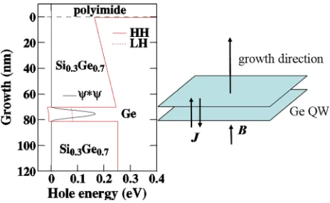
The band structure of the undoped Ge quantum wells was modeled using the 8 bandk.p.self-consistent device simula-tor17nextnano3. Figure1shows thenextnano3solution of the valence band at1 V forward bias with a thick gate dielectric on wafer A. The band off-set between the Ge quantum well and the Si0.3Ge0.7barriers for the heavy hole ground state is
0.26 eV. The solid black line is the self-consistent charge distribution with confinement to the 11 nm thick Ge quantum well. The heavy hole (HH) state forms the ground state with the unoccupied light hole (LH) state 94 meV higher in energy than the HH state. The Ge quantum well is compressively strained with a theoretical strain of 1.2% for the Ge well, Si0.3Ge0.7barrier combination. However, the measured strain in the case of the Ge well, Si0.2Ge0.8higher Ge content barrier
structures is0.65% due to a residual tensile strain in the bar-rier layer.13This effect will reduceDbut not change the inter-pretation of the spin-splitting properties significantly.
III. MEASUREMENTS
A. Introduction to electrical measurements
The magnetotransport measurements were made between 1.6 K and 350 mK using either a standard 4He variable tem-perature insert or a Heliox 3He insert. The temperature was measured directly at the sample with a calibratedCernox sen-sor in both cryostat systems. An AC excitation of between 10 and 100 nA was used for the source-drain current. Pre-amplifiers with100 gain and a 10 kHz bandwidth were used forqxxandqxyprior to lockin amplification at a frequency of 33 Hz. Gate voltages were applied with a Keithley 213 voltage source through a low pass filter.
B. The Hall effect
[image:3.612.322.554.61.204.2]Figure2(a)shows the Hall mobility (l) as a function of hole density (p) at 1.6 K for wafer A. Three separate cool downs (labeled 1–3) are shown that demonstrate the repro-ducibility and stability of the persistent photoconductivity
TABLE I. The properties of the two wafers reported in this paper.
Wafer Barrier material QW width (nm) p (1011cm2) l(cm2/V s)
(A) Si0.3Ge0.7 11 1.3 478 000
(B) Si0.2Ge0.8 13 0.9 209 000
FIG. 1. The valence band structure of device A calculated usingnextnano3 with a voltage of1 V on the surface. The charge distributionjW:Wjis plotted showing confinement to the Ge quantum well. The schematic shows the applied field and the quantization axis forJwith respect to the growth direction and the applied magnetic field (B) direction.
FIG. 2. (a) The Hall mobility as a function of hole density at 1.6 Kafter illu-mination in device A. Three separate cool downs are shown for comparison. (b) The two contact source-drain conductance and (c) hole density as a func-tion of top gate voltage at 1.6 K in device A.
[image:3.612.323.553.580.720.2] [image:3.612.50.299.716.765.2]effect. The fact thatlp1.0prior to the on-set of insulating behaviour (for p41010cm2) indicates a dominant scat-tering mechanism due to residual background acceptor impu-rities in the quantum well and buffer layers.18The two contact source-drain conductance, including contact series resistance, is70lS at Vg(top gate voltage)¼0 V although this can be increased to 250lS in enhancement without significant gate leakage current. Figure2(b) shows the source-drain conduc-tance after illumination showing a stable hole density. Full channel depletion is achieved atþ2 V, with a capacitance of
0.561011cm2/V from the Hall carrier density as a func-tion of top gate voltage (see Figure2(c)). This is close to the predicted capacitance value of 0.42 1011cm2/V, given the series capacitance contributions to the dielectric gate stack using the parameters in TableIIand the following equation:
dp dVg
1
¼e dGe eGe
þdSiGe eSiGe
þdpolyimide epolyimide
; (1)
where d is the layer thickness andeis the dielectric constant. The variable subscripts refer to the different dielectric mate-rials between the metal surface gate and the Ge quantum well. e is the unit of charge. This confirms the quantum well region is conducting rather than an interface or surface con-tribution. There is no screening of the gate field and no paral-lel conduction in the SiGe graded composition buffer layers or the Ge or Si cap at the surface. There is no drift of the pinch-off voltage or hysteresis in the conductivity versus gate voltage characteristic; i.e., there is no charge build-up at the surface of the polyimide dielectric.
C. The Shubnikov-deHaas effect
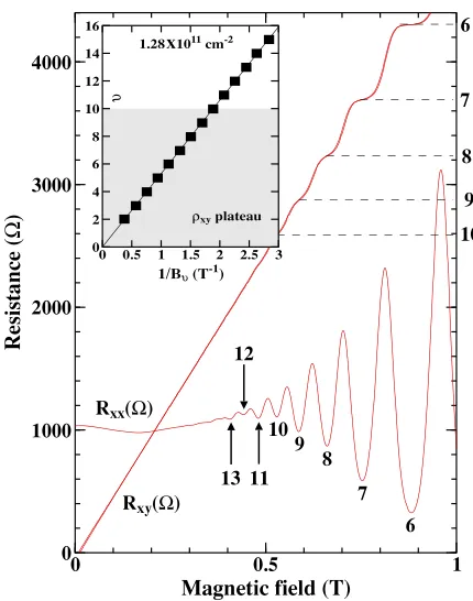
Magnetic fields (B) were applied in the growth direc-tion, perpendicular to the conducting plane andparallel to the total angular momentum vector J (see Figure 1 for a schematic of the geometry). An ungated device from wafer A was measured at 350 mK (see Figure3). This figure shows the Shubnikov-deHaas effect in qxx and the quantum Hall effect inqxyup to 1 T. The full data set was taken up to 12 T. A clear series of oscillations are observed down to filling fac-torst(hp/eB)15, where h is Planck’s constant with a sin-gle fundamental field (Bf) of 2.65 T, corresponding to p¼1.281011cm2. The inset of Figure3is a plot of the filling factor against inverse minima field position (1/Bt), showing that a single harmonic series is present with no evi-dence of beating, multiple frequencies or a second subband. The gradient of the line corresponds to the measured Bfvalue. The grey area in Figure3inset shows the region where quan-tum Hall plateaus are observed (withqxy¼h/te2), confirming the unique filling factor assignment. A fast Fourier transform
(FFT) of the oscillations in qxxshows a single fundamental field at Bf¼hp/e due to the dominance ofoddfilling factors in the Shubnikov-deHaas effect in the low field region. The lowest visible minima are at odd filling factors 13, 15, 17; this point is further discussed in Section IV and is fundamental to under-standing the spin-splitting behaviour in p-Ge. Any non-parabolicity in the Ge valence band could introduce harmonics of Bfin the FFT, but these are not seen at this hole density, where Ef2.7 meV. Non-sinusoidal Shubnikov-deHaas oscil-lations included in the field domain of the FFT can also produce additional harmonic peaks as previously reported7in p-Ge.
A magnetic field modulation system was used to measure analogue dRxx/dB and d2Rxx/dB2signals directly. A solenoid co-linear with the DC magnetic field was used that provided an AC magnetic field of 5.7 mT at 33 Hz. A lock-in amplifier was used to measure dRxx/dB at the fundamental 33 Hz. The second har-monic signal at 66 Hz corresponds to d2Rxx/dB2. The Rxx and
d2Rxx/dB2 signals can be compared on the same plot, for example, Figure4. The sensitivity of the magnetic field mod-ulation technique in measuring device B is demonstrated in Figure 4. The red curve is the DC qxxat 0.4 K and the green curve is the DC qxx at 1.6 K. At 1.6 K, even filling factor Shubnikov-deHaas minima>4 and odd minima>7 have disap-peared inqxx. In the analogue second derivative signal at 1.6 K (the dotted green curve), odd minima can still be observed for
[image:4.612.328.543.58.331.2]t>7 showing the increased sensitivity to oscillatoryqxx struc-ture. The random noise level in Figure4is less than the width of the red and green lines. There arenomultiple frequencies (i.e., peak splitting) in the FFT of dRxx/dB or d2Rxx/dB2from device A or B that would be characteristic of a Rashba spin-splitting. TABLE II. Dielectric properties associated with wafer A.
Material d (nm) er
Ge 8.5 16.0
Si0.3Ge0.7 70 14.8
polyimide 430 3.4
FIG. 3.qxxandqxyat low field and 360 mK in (ungated) device A after
illumination showing the prevalence of odd-minima inqxxat the on set of
[image:4.612.51.297.703.766.2]D. Gated transport measurements
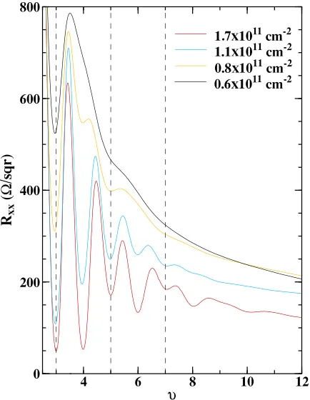
In Figure5,qxxis plotted as a function of filling factor in a series of gated measurements at 1.6 K in device A. At 0.61011cm2Shubnikov-deHaas minima are observed at
t¼3, 5, and 7 (the vertical dotted lines) with an even mini-mum only at the Shubnikov-deHaas fundamentalt¼2 posi-tion, not shown in the figure. Even minima (>2) start to develop as the carrier density is increased with the surface gate, for example, thet¼6 minimum starts to appear at 1.1
1011cm2. The dominance of odd minima is due to the large g-factor (g) in the HH states of the Ge valence band with the Zeeman splitting (DEss)¼3 glBB, comparable to the cyclotron energy (ÉeB/m*) in this material where m* is the effective hole mass andlBis the Bohr magneton. This is discussed further in SectionIV. The reduction of the energy gap at even filling factors in the Shubnikov-deHaas effect has been previously observed in lower mobility p-Ge super-lattices19 and p-SiGe quantum wells.20 The effect is clearer in lower mobility material with larger Landau level broaden-ing and is relatively unnoticed when p is>1.71011cm2. At 2 1011cm2 in the modulation doped Ge quantum well system,10 the prevalence of odd minima has gone although the spin-splitting is still the dominant exchange enhanced Zeeman effect.
Low filling factors were investigated in these wafers in magnetic fields up to 12 T. A fractional quantum Hall effect (fqhe) is observed at 350 mK corresponding to
t¼2/3 (at higher carrier density) and 1/3 (at lower carrier density) in device A. The momentum scattering rate 1/sp
(where sp is the momentum lifetime calculated from the transport mobility) is in the region of 70 GHz or less to observe the fqhe as a general rule from the literature over a range of semiconducting materials.21This corresponds to al>300 000 cm2/V s for the case of heavy holes in Ge, eas-ily achieved with p as low as0.81011cm2in device A.
In wafer A at high magnetic field (and 350 mK), a mag-netoresistance characteristic of the fqhe can be seen develop-ing in the lowest Landau level (see Figure 6). This figure shows rxxand rxy as a function of the filling factor at 350 mK from p¼0.78 to 1.61011cm2. Minima can be seen developing at 2/3 and 1/3 in rxx. These minima correspond to the formation of fractional plateau inrxyat 2/3(e2/h) and 1/3(e2/h). Higher mobility p-Ge material from the same growth system has shown a richer fqhe structure in the sec-ond Landau level22at lower temperatures and the low filling factor regime is not discussed further here.
E. Narrow channel arrays
[image:5.612.65.284.59.334.2]In a narrow channel, the loss of even filling factors in the Shubnikov-deHaas effect is even more pronounced. Figure 7shows the magnetoresistance in an array of nar-row channels with nominal physical widths of 3, 2, and 1lm from wafer A. The inset shows a low field FFT of the Shubnikov-deHaas oscillation in this device with the fun-damental field at hp/e due to the dominant Zeeman split-ting enhancing the odd filling factor minima in comparison to the even minima. The influence of the increased scatter-ing rate in the 2 and 1lm device channels can be seen as a clear loss of the minima at t¼4, leaving only a strong 3 FIG. 4. Magnetoresistance in device B with carrier density 91010cm2.
The odd filling factors (from 3 to 11) are indicated by the vertical dotted lines. The y-axis scale in the case ofd2Rxx/dB
2
[image:5.612.330.547.62.342.2]is in arbitrary units not the X/SQR units of the labeled y-axis. SQR is the length to width ratio of the Hall bar.
FIG. 5.qxxmeasurements at 1.6 K as a function of filling factor in device A
showing the development of the evenfilling factors with increasing hole density. At 61010cm2, only odd minima are observed att¼3, 5, and 7 (the vertical dashed lines).
and 5 (and 7) minima. This behavior is also confirmed when analogue dqxx/dB signals are directly measured by magnetic field modulation or by increasing the measurement tempera-ture. The saturation carrier density does not change with wire width due to the low density of surface states at the etched Ge sidewall.10The conducting wire width as opposed to the lithographic wire width could not be determined as the low field boundary scattering peak (see Ref. 10) was not well defined. However, the field extent over which a negative mag-netoresistance dominates does increase from 0.2 to 0.4 T (in Fig. 7) with decreasing mesa width but without quantitative numbers available for the conducting thickness and the deple-tion width.
IV. DISCUSSION
A. Zero magnetic field spin-splitting
The Ge quantum well is compressively strained and has HH (J¼3/2, mj¼63/2) character at the top of the valence band with the LH states (J¼3/2, mj¼61/2) higher in energy. In Section II, this HH-LH energy splitting was calculated as 94 meV; hence, there is a negligible LH contribution to the charge transport. The Rashba term in the Hamiltonian23,24for theC8vstates is given by
^
HRashbaC8v ¼b1ðkjjEÞ Jþb2ðkjjEÞ J3; (2)
where the total angular momentum J has components (Jx, Jy, Jz), J3 has components, (Jx3, Jy3, Jz3), and kjj has components (kx, ky, 0). The electric fieldEis in the growth direction with components (0, 0, Ez). In Eq. (2),b1 b2 with no linear k, spin-splitting for the HH band.23The HH spin-splitting is then given by:DEss¼2b1k3jj. However, the fundamental quantization axis for the angular momentumJ
is along the strain vector, perpendicular to the plane of the Ge quantum well. This means that the ground state HH spin orientation is out of plane with the higher energy LH spin states projected in-plane. If the in-plane momentum is kjj, then for a perpendicular electric fieldE
ðkjjJÞ E 0; kjjJ 0; (3)
[image:6.612.330.545.59.356.2]and a Rashba spin-splitting cannot exist in the strained QW for the out-of-plane HH angular momentum orientation. This FIG. 6.rxxandrxyas a function of the filling factor at 350 mK for hole
den-sities from 81010cm2to 1.61011cm2in device A. The maximum applied magnetic field is 12 T. The dashed diagonal line inrxycorresponds
tote2/h.
FIG. 7.qxxup to 4 T in a series of narrow channels (width 1 to 3lm as
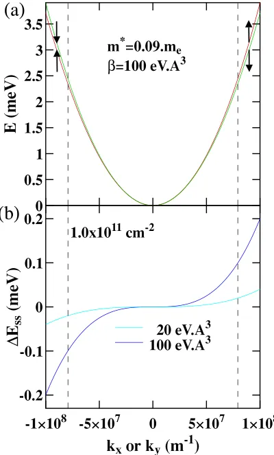
[image:6.612.76.270.61.534.2]partly explains the lack of Rashba spin-splitting in devices where there is negligible coupling to the LH states. In Figure
8(a), the calculated band structure for the HH state is plotted as a function of in-plane momentum (kx or ky) assuming m*¼0.09me from Ref. 25 and a b1 value of 100 eV A˚
3
from Ref. 7. The spin projection conserves time reversal symmetry with the state at energy E(þk, ")¼E(k, #). In Figure8(b), the energy splittingDEss¼E(k,")E(k, #) is plotted as a function of k. The vertical dotted lines corre-spond to the Fermi wave vector for p¼11011cm2. Two values ofb1are used from the literature, 20 eV A˚3(the high-est value measured in Ref. 6) and 100 eV A˚3(Ref. 7) as a comparison. The predicted spin-splitting at 11011cm2is in the range 0.02 meV–0.1 meV. TheDEssvalue corresponds to a thermal energy kBT (where kBis Boltzmann’s constant and T is the temperature) of 0.23 K (with b1 from Ref. 6) with the actual measurement temperature of7DEssand hence a thermal broadening of any potential Rashba effect.
The previous theoretical work on the Rashba effect23,24 in the valence band predicts a cubic Rashba effect for the HH state but ignores the fact that strain provides the main quantization axis for the angular momentum states. In the Ge quantum well, the SIA contribution to the spin-splitting is controlled by the effective potential steps at the Ge-Si1xGex interfaces and there is very little contribution from the applied gate voltage or the built-in electric field in
determining the spin-splitting, i.e.,DEssshould be insensitive to the applied gate voltage. Previous experimental measure-ments6–9 have demonstrated a small to moderate Rashba effect with only a weak dependence on applied electric field, in disagreement to what is measured here.
B. Spin-splitting in finite magnetic field
The Zeeman energy term for the overall Luttinger Hamiltonian26in the valence band with J¼3/2 in an applied per-pendicular magnetic field B is given by the following equation:
^
HZeemanC8v ¼2jlBBJþ2qlBBJ3: (4)
The first term in Eq.(4)is an isotropic term (with axial sym-metry defined by J) and this dominates over the second anisotropic term. 2j is the g-factor, determined from the Luttinger formulation,24,26 and the band parameter q is cal-culated fromkptheory. This is an energy correction due to coupling to remote (conduction) bands. In the Ge HH valence band, qjand Eq.(4)reduces toH^C8v¼glBBJ with DEss¼3glBB the dominant spin-splitting term in an applied magnetic field. In the Luttinger model,24,26the mixing of HH-LH states in applied magnetic field is negligible unless there is a magnetic field component in-plane. Previous meas-urements27 on acceptor states in narrow Ge quantum wells have made use of the fact that an in-plane magnetic field can split the LH states while preserving the HH (mj¼63/2) degeneracy.
The effective mass7,25 and the g-factor25,28 have been determined in p-Ge as 0.0960.02 mewith g in the range from 4 to 7. With these parameter values from the literature, the Zeeman splitting is comparable to the cyclotron energy split-ting, with DEss
hxc ¼
3 2g
m
me 0:860:4, where the cyclotron fre-quency xc¼eB/m*. This leads to the dominant anomalous Zeeman splitting effect particularly at odd filling factors that are observed in Figure 5. The Zeeman spin-split peak of the Shubnikov-deHaas oscillation FFT is then at hp/e. This fre-quency identification in the Shubnikov-deHaas effect can be seen in the inset of Figure7. The dominance of odd minima in the Shubnikov-deHaas effect disappears for p21011cm2. This is for two reasons. First, the “disordered” Landau level width is proportional to B1/2, so at higher hole density the Shubnikov-deHaas minima occur at higher real B and the Landau levels have a reduced width. This would tend to reverse the effects of losing the even filling factor gaps in the density of states at low carrier density. The second effect is that influenced by the exchange interaction. The Lande g-factor that determines the Zeeman energy gap is exchange energy enhanced, and at higher B, the exchange energy reduces (there is less spatial wavefunction overlap) decreas-ing the Zeeman energy gap. This would have the effect of increasing the dominance of even minima gaps that can be seen developing at p 1.71011cm2in Figure5.
V. SUMMARY
The compressively strained Ge quantum well guarantees that the out-of-plane heavy hole angular moment component FIG. 8. (a) The band structure in the heavy hole band in Ge forb1¼100 eV
A˚3, showing the 63/2 angular momentum states. (b) The spin-splitting energy as a function of in-plane wave vector with the predictedb1parameter
from Refs.6and7for comparison.
[image:7.612.73.273.388.719.2]mj¼63/2 does not couple to the linear in-plane momentum via a linear (or cubic) Rashba spin-orbit effect with p1011cm2. There is no measurable Rashba spin-orbit coupling unless there is HH-LH mixing of the wavefunction caused by compressive strain, high p-type doping, or applied in-plane magnetic field. In the compressively strained Ge quantum well-SiGe barrier combination, this mixing effect is ruled out by the large energy splitting between the mj63/2 and 61/2 states. The dominance of odd minima qxx in the Shubnikov-deHaas effect is due to the anomalous Zeeman splitting of the heavy hole state compared to the cyclotron energy. The effects reported in this work are also applicable in the InxGa1xSb-GaSb strained p-type quantum well system, where the heavy hole spin state is projected in the growth direction, leading to spin confinement.29 Undoped p-Ge strained quantum wells behave as a spin63/2 system with the spins oriented in the strain (growth) direction. Any Rashba spin-orbit coupling effect is likely to be due to LH states that can be occupied depending on the details of the strain in the device, the confining potential, and the p-type doping level.
ACKNOWLEDGMENTS
This work programme at the University of Cambridge and Warwick University is funded by the EPSRC, “Spintronic device physics in Si/Ge heterostructures,” EP/ J003263/1, and a platform Grant No. EP/J001074/1.
1
See http://www.itrs2.net/2013-itrs.html for International Technology Roadmap for Semiconductors (ITRS2).
2I. L. Markov,Nature512, 147 (2014). 3P. S. Goley and M. K. Hudait,Materials
7, 2301 (2014).
4
C. Shen, T. Trypiniotis, K. Y. Lee, S. N. Holmes, R. Mansell, M. Husain, V. Shah, H. Kurebayashi, I. Farrer, C. H. de Groot, D. R. Leadley, G. Bell, E. H. C. Parker, T. Whall, D. A. Ritchie, and C. H. W. Barnes,Appl. Phys. Lett.97, 162104 (2010).
5S. Dushenko, M. Koike, Y. Ando, T. Shinjo, M. Myronov, and M.
Shiraishi,Phys. Rev. Lett.114, 196602 (2015).
6
R. Moriya, K. Sawano, Y. Hoshi, S. Masubuchi, Y. Shiraki, A. Wild, C. Neumann, G. Abstreiter, D. Bougeard, T. Koga, and T. Machida,Phys. Rev. Lett.113, 086601 (2014).
7C. Morrison, P. Wisniewski, S. D. Rhead, J. Foronda, D. R. Leadley, and
M. Myronov,Appl. Phys. Lett.105, 182401 (2014).
8
J. Foronda, C. Morrison, J. E. Halpin, S. D. Rhead, and M. Myronov, J. Phys.: Condens. Matter27, 022201 (2015).
9M. Failla, M. Myronov, C. Morrison, D. R. Leadley, and J. Lloyd-Hughes,
Phys. Rev. B92, 045303 (2015).
10
P. J. Newton, J. Llandro, R. Mansell, S. N. Holmes, C. Morrison, J. Foronda, M. Myronov, D. R. Leadley, and C. H. W. Barnes,Appl. Phys. Lett.106, 172102 (2015).
11R. Winkler, D. Culcer, S. J. Papadakis, B. Habib, and M. Shayegan,
Semicond. Sci. Technol.23, 114017 (2008).
12
R. Pillarisetty,Nature479, 324 (2011).
13A. Dobbie, M. Myronov, R. J. H. Morris, A. H. A. Hassan, M. J. Prest, V.
A. Shah, E. H. C. Parker, T. E. Whall, and D. R. Leadley, Appl. Phys. Lett.101, 172108 (2012).
14
M. Myronov, C. Morrison, J. Halpin, S. Rhead, C. Casteleiro, J. Foronda, V. A. Shah, and D. Leadley, Jpn. J. Appl. Phys., Part 1 53, 04EH02 (2014).
15
M. Myronov, C. Morrison, J. Halpin, S. Rhead, J. Foronda, and D. R. Leadley,Solid-State Electron.110, 35 (2015).
16O. A. Mironov, A. H. A. Hassan, R. J. H. Morris, A. Dobbie, M. Uhlarz,
D. Chrastina, J. P. Hague, S. Kiatgamolchai, R. Beanland, S. Gabani, I. B. Berkov, M. Helm, O. Drachenko, M. Myronov, and D. R. Leadley,Thin Solid Films557, 329 (2014).
17See http://www.nextnano.de/nextnano3/ for nanodevice simulator
soft-ware,nextnano3. 18
A. Gold,Phys. Rev. B35, 723 (1987).
19
Yu. G. Arapov, N. A. Gorodilov, V. N. Neverov, G. I. Kharus, N. G. Shelushinina, O. A. Kuznetsov, L. K. Orlov, R. A. Rubtsova, and A. L. Chernov, JEPT Lett.59, 245 (1994).
20
P. T. Coleridge, A. S. Sachrajda, H. Lafontaine, and Y. Feng,Phys. Rev. B
54, 14518 (1996).
21B. A. Piot, J. Kunc, M. Potemski, D. K. Maude, C. Bethausen, A. Vogl, D.
Weiss, G. Karczewski, and T. Wojtowicz,Phys. Rev. B 82, 081307(R) (2010).
22
Q. Shi, M. A. Zudov, C. Morrison, and M. Myronov,Phys. Rev. B91, 241303(R) (2015).
23R. Winkler, H. Noh, E. Tutuc, and M. Shayegan,Phys. Rev. B
65, 155303 (2002).
24
R. Winkler,Phys. Rev. B62, 4245 (2000).
25I. B. Berkutov, V. V. Andrievskii, Yu. F. Komnik, O. A. Mironov, M.
Myronov, and D. R. Leadley,Low Temp. Phys.35, 141 (2009).
26
J. M. Luttinger,Phys. Rev.102, 1030 (1956).
27
K.-M. Haendel, R. Winkler, U. Denker, O. G. Schmidt, and R. J. Haug, Phys. Rev. Lett.96, 086403 (2006).
28
J. C. Hensel,Phys. Rev. Lett.21, 983 (1968).
29