FABRICATION AND CHARACTERIZATION OF SILICON
NITRIDE THIN FILM PLANAR WAVEGUIDES PRODUCED BY RF
MAGNETRON SPUTTERING TECHNIQUE
UZAIR MAJEED
A thesis submitted in partial
fulfillment of the requirement for the award of the degree of Doctor of Philosophy of Science
Faculty of Science, Technology and Human Development Universiti Tun Hussein Onn Malaysia
iii
DEDICATION
iv
ACKNOWLEDGEMENTS
I would like to express my deepest appreciation to Assoc. Prof. Dr. Mohd. Kamarulzaki Mustafa for his mentorship, kindness and patience during my entire educational journey. Without his valuable assistance, this work wouldn’t have been completed.
Special thanks for my parents Mr. and Mrs. Majeed Uddin Siddiqui for their immense support and precious love who was always standing by me in my hard times during this work.
I am indebted to my wife and my son Muhammad Safwan for their patience, understanding and care.
I would like to acknowledge the valuable pat on my back of my brothers Farrukh Majeed, Osama Majeed, Talha Majeed, Hammas Majeed and my sister Mrs. Muhammad Waseem.
I would like to extend my thanks to staff and colleagues of Micro and Nano Technology – Shamsuddin Research Center (MiNT-SRC) for all their support during my study.
Many thanks to my lab mates Younas Iqbal and Auwal Mahmood for the fun we had together. I really enjoyed their company.
These acknowledgements wouldn’t be completed without mentioning my friends Habib Shah, Fazal-e-Wadood, Fazal-e-Akbar and Haslinda binti Abdul Hamid who introduced Malaysian lifestyle and culture to me.
v
ABSTRACT
Silicon nitride based planar waveguides play an important role in biosensing applications. Conventional fabrication of silicon nitride waveguides utilizes the chemical vapor deposition (CVD) technologies. Silicon nitride waveguide fabrication through magnetron sputtering is still unexplored and a few literatures are available only on microelectronic and optoelectronic applications. In current study, the silicon nitride thin film planar waveguides were fabricated on SiO2 coated silicon substrates
vi
ABSTRAK
vii
TABLE OF CONTENTS
TITLE i
DECLARATION ii
DEDICATION iii
ACKNOWLEDGEMENTS iv
ABSTARCT v
TABLE OF CONTENTS vii
LIST OF TABLES xi
LIST OF FIGURES xiii
LIST OF SYMBOLS AND ABBREVIATIONS xvii
LIST OF PUBLICATIONS xx
CHAPTER 1 INTRODUCTION
1.1 Introduction 1
1.2 Background of study 3
1.3 Problem statement 6
1.4 Objectives of the study 7
1.5 Scopes of the study 7
CHAPTER 2 LITERATURE REVIEW
2.1 Introduction 9
2.1.1 Modes in planar waveguides – physical
optic approach 9
2.1.2 Modes in planar waveguides – ray optic
approach 13
viii 2.3 Waveguide fabrication by sputtering technique 19
2.3.1 Sputtering process considerations 21
2.3.1.1 Sputtering yield 21
2.3.1.2 Mean free path 22
2.3.2 Applications of sputtering technique 22 2.4 Effect of sputtering parameters on thin film
properties 24
2.4.1 Effect of sputtering power 24
2.4.2 Effect of sputtering pressure 25
2.4.3 Effect of target to substrate distance 26
2.5 Characterization techniques 27
2.5.1 X-ray diffraction 27
2.5.2 Field emission – scanning electron
micrsocopy 31
2.5.3 Energy dispersive x-ray analysis 33
2.5.4 Surface profiling 34
2.5.5 Atomic force microscopy 35
2.5.6 Spectral reflectance 37
2.5.7 UV-VIS spectroscopy 40
2.5.8 Spectroscopic Ellipsometry 43
2.5.9 Prism coupling technique 44
CHAPTER 3 METHODOLOGY
3.1 Introduction 47
3.2 Sample preparation 49
3.2.1 Substrate cleaning 49
3.2.2 Fabrication of silicon dioxide lower
cladding 49
3.3 Fabrication of silicon nitride core 51
3.3.1 Substrate cleaning 51
3.3.2 Sputtering deposition system 51
3.3.2.1 Deposition chamber 52
ix 3.3.2.3 Sputtering deposition controller 55 3.3.3 Pre-s puttering of Si3N4 target 56
3.3.4 Variation of sputtering parameters 56 3.3.4.1 Variation of sputtering power 57 3.3.4.2 Variation of sputtering pressure 57 3.3.4.3 Variation of target to substrate
distance 58
3.4 Characterization of silicon nitride thin films 59
3.4.1 Physical characterization 59
3.4.1.1 Field emission – scanning electron
micrsocopy 59
3.4.1.2 Atomic force microscopy 61
3.4.1.3 X-ray diffraction 63
3.4.1.4 Surface profiling 64
3.4.2 Optical characterization 65
3.4.2.1 Spectral reflectance 65
3.4.2.2 UV-VIS spectroscopy 66
3.5 Fabrication of waveguide through selected
sputtering parameters 67
3.6 Characterization of silicon nitride thin film planar
waveguide 68
3.6.1 Spectroscopic ellipsometry 68
3.6.2 Prism coupling 69
CHAPTER 4 RESULTS AND DISCUSSION
4.1 Effect of sputtering parameters on surface
morphology 71
4.1.1 Surface structure 71
4.1.2 Surface topography 74
4.1.3 Growth rate 83
x 4.3 Effect of sputtering parameters on chemical
composition 88
4.4 Effect of sputtering parameters on optical properties 94 4.4.1 Refractive index and extinction co-efficient 94
4.4.2 Optical bandgap 97
4.5 Selection of sputtering parameters for the fabrication
of asymmetric planar waveguide 99
4.6 Characterization of asymmetric planar silicon nitride
waveguides 101
4.6.1 Ellipsometric analysis 101
4.7 Optical waveguides loss measurements 104
CHAPTER 5 CONCLUSION AND FUTURE RECOMMENDATIONS
5.1 Conclusion 107
5.2 Future recommendations 109
REFERENCES
VITA
xi
LIST OF TABLES
2.1 Applications of DC sputtering technique 23
2.2 Applications of RF sputtering technique 23
2.3 Description of surface profile parameters 37
3.1 Piranha cleaning parameters 49
3.2 Deposition conditions during lower cladding fabrication 50
3.3 The process parameters for pre-sputtering of Si3N4 target 56
3.4 Deposition conditions with variation in sputtering power 57 3.5 Deposition condition with variation in sputtering pressure 58 3.6 Deposition conditions with variation in target to substrate
distance 59
3.7 Parameters for fabrication of asymmetric planar
waveguide 68
4.1 Roughness parameters of deposited thin films at various
sputtering powers 76
4.2 Roughness parameters of deposited thin films at various
sputtering pressures 79
4.3 Roughness parameters of deposited thin films at various
target to substrate distance 82
4.4 Growth rate of sputtered films at different sputtering
powers 84
4.5 Growth rate of sputtered films at different sputtering
pressures 84
4.6 Growth rate of sputtered films at different target to
substrate distance 85
4.7 Percentage composition of samples deposited at different
xii
4.8 Percentage composition of samples deposited at different
sputtering pressure 90
4.9 Percentage composition of samples deposited at different
target to substrate distance 92
4.10 Optical properties of silicon nitride layer in planar
xiii
LIST OF FIGURES
1.1 Illustration of symmetric planar waveguide 1
2.1 Planar waveguide structure infinite in y and z directions 10 2.2 Modes in planar waveguide (Hunsperger, 2002) 11 2.3 Ray-optic representation of optical waveguide 13 2.4 Geometrical relationships of optical waveguide
propagation constants 14
2.5 Ray-optic approach for (a) air radiation mode, (b)
substrate radiation mode, (c) guided mode 15
2.6 An approach to determine scattering loss in planar
waveguide 18
2.7 Interactions of ion with target surface (Ohring, 2001) 20 2.8 Reflection of x-rays from two successive crystal planes 28
2.9 A schematic of XRD equipment 28
2.10 A typical XRD spectra of silicon (211) wafer before and after several hours of etching in KOH solution
(Abdel-Hady et al.,2013) 30
2.11 A schematic of FESEM internal structure 32
2.12 A typical EDX spectrum of thin film sample 33
2.13 A schematic of surface profiling technique 34 2.14 A schematic of AFM (Barattin & Voyer, 2008) 35 2.15 A typical 3D AFM image of silicon nitride thin film 36 2.16 A schematic of spectral reflectance measurement system 38
2.17 An illustration of the components of an electromagnetic
wave (Tomkins & McGahan, 1999) 39
2.18 An illustration of light reflection from a single interface
(Tomkins & McGahan, 1999) 39
xiv
2.20 A schematic of spectroscopic ellipsometer 43
2.21 A schematic of prism coupler setup 45
2.22 A schematic of loss measurement setup using prism
coupler technique 46
3.1 Flow chart of the fabrication and characterization of
silicon nitride thin films for waveguide applications 48
3.2 Thermal oxidation furnace (MOD-LAB, USA) 50
3.3 Ultrasonic cleaning apparatus (Power sonic 405, Hwashin,
Korea) 51
3.4 Magnetron sputtering system (SNTEK, KOREA) 52
3.5 Outlook of deposition chamber of magnetron sputtering
system 53
3.6 Cross-section of magnetron sputtering deposition chamber 54
3.7 Si3N4 Sputtering target used in this study 55
3.8 Controller of magnetron sputtering deposition system 55
3.9 A schematic of target to substrate distance modification 58
3.10 Field emission – scanning electron microscope (7600F,
JEOL, Japan) 60
3.11 Sputter coater (JFC1600, JEOL, Japan) 60
3.12 Atomic force microscopy system (NC 100 Park systems,
USA) 62
3.13 X-ray diffractometer (Xpert3, PANalytical, USA) 63
3.14 Surface profiler (Alpha Step, KLA TENCOR, USA) 64
3.15 Thin film analyzer (F-20, Filmetrics USA) 66
3.16 UV-VIS spectrophotometer (UV1800, SHIMADZU,
Japan) 67
3.17 Spectroscopic ellipsometer (SE2000 Semilab, Hungary) 69
3.18 Prism coupler (2010/M, METRICON, USA) 70
4.1 Surface morphology of silicon nitride thin films at various sputtering powers: (a) 100 W (b) 150 W (c) 200 W (d) 250
W (e) 300 W 72
4.2 Surface morphology of silicon nitride thin film at various sputtering pressures: (a) 5 mTorr (b) 7.5 mTorr (c) 10
xv 4.3 Surface morphology of deposited thin films at various
target to substrate distances: (a) 8 cm (b) 10 cm (c) 12 cm
(d) 14 cm 74
4.4 Surface topology of silicon nitride thin films at different sputtering power: (a) 100 W (b) 150 W (c) 200 W (d) 250
W (e) 300 W 75
4.5 Surface roughness of silicon nitride thin films at different
sputtering powers 77
4.6 Surface topology of silicon nitride thin films at different sputtering pressure: (a) 5 mTorr (b) 7.5 mTorr (c) 10
mTorr (d) 12.5 mTorr (e) 15 mTorr 78
4.7 Surface roughness of silicon nitride thin films at different
sputtering pressures 80
4.8 Surface topology of silicon nitride thin films at different target to substrate distance: (a) 8 cm (b) 10 cm (c) 12 cm
(d) 14 cm 81
4.9 Surface roughness of silicon nitride thin films at different
target to substrate distance 83
4.10 XRD spectra of silicon nitride thin films at various sputtering parameters: (a) sputtering power (b) sputtering
pressure (c) target to substrate distance 87
4.11 EDX spectrum of silicon nitride thin films at various
sputtering powers: 89
4.12 Nitrogen content increase at various sputtering power 90
4.13 EDX spectrum at different sputtering pressures: (a) 5 mTorr (b) 7.5 mTorr (c) 10 mTorr (d) 12.5 mTorr (e) 15
mTorr 91
4.14 Variation in Nitrogen content at different sputtering
pressures 92
4.15 EDX spectrum obtained at various target to substrate
distance: 93
4.16 Variation in nitrogen content at different target to substrate
xvi
4.17 Refractive index and extinction co-efficient at diverse sputtering parameters: (a) sputtering power (b) sputtering
pressure (c) target to substrate distance 96
4.18 Optical investigations of thin films deposited at various sputtering pressure: (a) Transmission spectra (b)
absorption coefficient (c) Tauc’s plot (d) Optical band gap 98 4.19 Optical investigations of thin films deposited at various
target to substrate distance: (a) Transmission spectra (b)
absorption coefficient (c) Tauc’s plot (d) Optical band gap 99 4.20 Measured and fit values of Ψ for the waveguide fabricated
at 300 W 101
4.21 Measured and fit values of Δ for the waveguide fabricated
at 300 W 102
4.24 Refractive index dispersion of the waveguide fabricated at
300 W 103
4.25 Extinction co-efficient dispersion of the waveguide
fabricated at 300 W 103
4.28 Modes obtained at λ = 448 nm 104
xvii
LIST OF SYMBOLS AND ABBREVIATIONS
dc - Collision diameter
e - Charge of electron
E - Electric field vector
H - Magnetic field vector h - Thickness of core is - Current density
k - Wave vector
k - Extinction co-efficient
m - Mode of propagation
nc - Refractive index of upper cladding
nf - Refractive index of core
ns - Refractive index of lower cladding
r - Radius vector
v - Velocity of light in vacuum ve - Velocity of electron
α - absorption co-efficient β - Propagation constant ω - Frequency of light ωc - Cutoff frequency
λo - Wavelength of light in vacuum
λc - Cutoff wavelength
λmfp - Mean free path
φ - Angle of light ray w.r.t normal to interface plane Δn - Refractive index difference between core and cladding AFM - Atomic Force Microscopy
xviii
B - Magnetic field
C - Capacitance
CVD - Chemical Vapor Deposition CRT - Cathode Ray Tube
D - Dimension
DC - Direct Current DI - Deionized Water E1 - Energy of incident ion
Eb - Surface binding energy
EDX - Energy Dispersive X-ray
FESEM - Field Emission Scanning Electron Microscopy GM/V - Gas Main Valve
HCG - Human Chorionic Gonadotropin IGZO - Indium Gallium Zinc Oxide IPA - Iso Propyle Alcohol
ITO - Indium Tin Oxide
ITiO - Indium doped Titanium Oxide
LPCVD - Low Pressure Chemical Vapor Deposition M1 - Mass of incident ion
M2 - Mass of target atom
MiNT-SRC - Micro and Nano Technology Shamsuddin Research Center NA - Avogadro’s number
NIR - Near Infra Red ONO - Oxide Nitride Oxide
P - Pressure
PECVD - Plasma Enhanced Chemical Vapor Deposition PVD - Physical Vapor Deposition
R - Ideal gas consyant RF - Radio Frequency
SCCM - Standard Cubic Centi Meter S - Sputtering yeild
SR - Spectral Reflectance
STP - Standard Temperature Pressure
xix TE - Transverse Electric
TM - Transverse Magnetic TMP - Turbo Molecular Pump TIR - Total Internal Reflection T/V - Throttle Valve
UTHM - University Tun Hussein Onn Malaysia UV-VIS - Ultra Violet – Visible
W - Watt
xx
LIST OF PUBLICATIONS
Mustafa, M. K., Majeed, U., & Nayan, N. (2015). “Characterization of silicon nitride waveguide produced by RF sputtering technique.” Malaysian Technical Universities Conference on Engineering and Technology (MUCET), Johor Bahru, Johor.
Majeed, U., Mustafa, M. K., & Nayan, N. (2015). Effect on silicon nitride thin films properties at various pressure of RF magnetron sputtering. Malaysian Journal of Fundamental and Applied Sciences, 11(2). 1-5.
CHAPTER 1
INTRODUCTION
1.1 Introduction
[image:20.595.124.514.523.630.2]The propagation of electromagnetic radiations in a homogeneous media has been a subject of interest because of its wide range applications. The phenomenon is described as electromagnetic wave guiding and the media is called waveguide. Planar or slab waveguide is the simplest structure that supports electromagnetic wave guiding. It is a multilayer structure in which a high refractive index media is sandwiched between low refractive media in planar geometry. An illustration of symmetric planar waveguide is shown in Figure 1.1.
Figure 1.1: Illustration of symmetric planar waveguide
According to Figure 1.1, ns, nf and nc are the refractive indices of lower
cladding, core and upper cladding respectively such that nf > ns≥ nc and ‘h’ is the
thickness of core layer. The light beam is coupled with the angle larger than the Upper cladding, nc
Core, nf
2 critical angle, it is confined in the core layer due to total internal reflection (TIR) from the interface.
Planar optical waveguides based sensing devices with high sensitivity, selectivity and rapid detection have already been demonstrated for clinical, environmental, industrial and military applications (Duval et al., 2012; Long et al., 2013). The sensitivity of planar waveguides has a direct relation with the refractive index of core layer. Due to this, the high refractive index materials such as TiO2,
Ta2O5, Nb2O5 and Si3N4 have attracted the researcher’s attention because of their low
propagation losses and high stability (Aquino et al., 2013; Bauters et al., 2011; Bradley et al., 2010; Muttalib et al.,2014).
Silicon nitride is one of the promising ceramic materials that was developed in 1960`s and 70`s in search of dense, highly stable and tough materials. The remarkable chemical, mechanical and electronic properties of silicon nitride widen it scope to numerous applications such as anti reflective coatings, dynamic random access memory, gate dielectrics in field effect transistors, protective coatings and waveguide devices (Signore et al., 2012). The properties such as high and tunable refractive index, known surface chemistry and low propagation losses fascinated researchers to exploit these films for development of highly sensitive waveguide based devices for sensing purposes.
Waveguide fabrication is the most crucial step in developing an effective device. Fabrication techniques can be categorized as chemical vapor deposition (CVD) and physical vapor deposition (PVD). The deposition of thin films using CVD techniques is done by exposing the substrates to one or more volatile precursors which either react or decompose on the substrate surface. In PVD techniques, physical processes such as high temperature vacuum evaporation with subsequent condensation or plasma sputter bombardment are exploited to deposit the required thin films.
3 literatures (de Castro et al., 2012; Yuste et al., 2012). Sputtering parameters have significant influences on the deposited thin film properties.
Preparation of silicon nitride films by other methods such as low pressure chemical vapor deposition (LPCVD), sol gel, thermal evaporation, plasma enhanced chemical vapor deposition (PECVD), ion plating and magnetron sputtering also has been reported. (Ali, Khan, & MatJafri, 2015; Karouta et al., 2012; Morin et al., 2012). The films deposited by magnetron sputtering show a delicate control on film properties with variation in deposition parameters. The properties such as growth rate, refractive index, surface roughness, film homogeneity, surface density and chemical composition have imperative effect in development of planar waveguides. Precise control gives the opportunity for optimization of deposition parameters to produce low loss planar optical waveguides.
1.2 Background of study
Magnetron sputtering is one of the PVD process to deposit thin films of virtually all materials due to availability of sputtering targets commercially. Silicon nitride thin films are under study due to its remarkable structural, electrical and optical properties which could be use for several applications.
Planar waveguide is a multiple layered structure used to confine light and pass over the required distance. The light is incident on a transparent interface separating two mediums of different refractive indices. Light refract through the interface along with partial reflection. Increasing incident angle above the critical angle gives the complete reflection from interface, name as total internal reflection (TIR). The wave guiding phenomenon is based on TIR for guiding the light over a required path.
4 al., 2014). This probing technique gave rise to several detection protocols such as phase modulation and intensity modulation for sensing application.
Heideman and colleagues first demonstrated the silicon nitride based oxide/nitride/oxide (ONO) waveguide in 1991. The fabrication of ONO waveguide structure was started with growing of silicon dioxide lower cladding by thermal oxidation technique on silicon substrates. A core layer of silicon nitride was deposited through LPCVD technique. The structure was completed by depositing silicon dioxide upper cladding through PECVD technique. They utilized ONO structure for the detection of 2.5 ng/ml of Human Chorionic Gonadotropin (HCG). The detection protocol used for this experiment was phase modulation with a phase shift of 0.6 π (Heideman, Kooyman, & Greve, 1991).
Schipper from the same group fabricated the ONO structure from the same procedure and utilized it to develop a rather simple detection protocol. The ONO structure was partly covered with upper cladding. Any immune reaction occurred in uncovered surface of sensor resulted a change in critical angle. Therefore, the sensor was named as critical sensor (Schipper et al., 1995).
Shirshov with his colleagues developed the ONO structure with same procedure in 1998. They exploited ONO waveguide as planar polarization interferometer. The detection protocol was based on measuring the polarization state of light beam after the interaction with immunoreactions. The sensor was able to detect as low as 10 ng/ml concentration (Shirshov et al., 1998). Nabok’s group exploited the ONO waveguide fabricated by the same method for the detection of 10 ppb of imidacloprid pesticide using the intensity modulation detection protocol (Nabok, Haron, & Ray, 2003).
The conventional fabrication of ONO waveguide involves three deposition technologies. The first layer of SiO2 lower cladding is grown by thermal oxidation on
silicon substrates followed by the silicon nitride core layer deposition by LPCVD. Then a protective upper cladding of SiO2 is deposited by PE CVD technique.
The thermal oxidation technique is a diffusion based process executed at temperature >1000oC using silicon substrates in oxygen ambient. The reaction takes place as presented in Equation 1.1.
i O2
high temp.
5
Hereafter, silicon nitride deposition on SiO2 substrates is performed by LPCVD
technique. Either silane (SiH4) or dichlorosilane (SiH₂Cl₂) gas is used as silicon
precursor with ammonia gas. The reaction takes place at temperature > 600oC as shown in Equation 1.2.
i N high temp. i N 12 2 (1.2)
Further the SiO2 upper cladding layer is deposited using PECVD technique in
silane and nitrogen filled environment. The reaction takes place as shown in Equation 1.3 at temperatures lower than LPCVD due to plasma enhancement.
i 2N2O
high temp.
iO2 2N2 2 2 (1.3)
The waveguide structure showed very low propagation losses. The refractive indices of silicon dioxide upper and lower cladding layer was measured as n = 1.46. The refractive index of silicon nitride core layer was n ~ 2.0. That made the refractive index contrast Δn ~ 0.5. The deposited films are usually high in density. However, despite of producing high quality optical waveguides, the conventional fabrication technology bears some disadvantages as follows: the involvement of toxic gases, incorporation of H2 gas which causes the degradation of optical and
structural properties and elevated temperatures that are inevitable for H2 removal.
Study shows the silicon nitride deposition by reactive magnetron sputtering technique using Si sputtering target in N2 ambient (Mousinho et al., 2012). The films
were deposited at low temperatures and were free of hydrogen. Therefore sputtering technique has an advantage over current fabrication technology as simple, safe and sequential process. However several sputtering parameters need to optimize in order to produce the good quality waveguide.
co-6 sputtering of stochiometric silicon nitride and silicon oxide sputtering targets at room temperature. However, the author observed high propagation losses when used the stochiometric silicon nitride target due to silicon rich nature of deposited films. Tiwari and Chandra (Tiwari & Chandra, 2011) deposited the silicon nitride thin films at room temperature for mechanical applications. The resultant films are reported with refractive indices greater than 1.8 without substrate heating. This study opened the possibility of optical waveguide fabrication using the stochiometric silicon nitride sputtering target.
1.3 Problem statement
Since the application of silicon nitride thin film as a planar waveguide for sensing applications, the features such as sensitivity, miniaturization, immobilization protocols and detection techniques are being improved. However there is no improvement observed in waveguide fabrication technology. Conventional CVD fabrication provides good quality optical waveguides but it inherits high deposition temperature (> 400oC). Silicon nitride thin films deposited at low temperatures by CVD technology are usually porous, unstable and contain a large amount of hydrogen (Karouta et al., 2012) . Another disadvantage of CVD technology is involvement of toxic gases such as silane, dicholorosilane and ammonia.
Sputtering technique is capable of deposit silicon nitride at low temperatures. Moreover, it doesn`t requires reactive toxic gases (Ruchi Tiwari & Chandra, 2011) and hence the procedure is environment friendly. Fabrication and characterization of silicon nitride in reactive sputtering regime which is sputtering of Si target in presence of N2 gas, has already been published extensively. However, the reactive
sputtering also has some limitation such as low deposition rate, poisoning of target and possibility of impurity incorporation. Contrary to this, non reactive sputtering, that is, fabrication by sputtering of stochiometric Si3N4 could be a promising
7 efficient planar optical waveguides but also aid the other applications such as microelectronics and optoelectronics as these fields also exploit the CVD fabricated silicon nitride thin films up to this time.
1.4 Objectives of the study
This research focused on investigating the magnetron non reactive sputtering technique as an alternative to conventional CVD technology to fabricate silicon nitride based optical waveguides. Following objectives to be studied during research work are as follows:
(i) To fabricate silicon nitride thin films at various sputtering powers, pressures and target to substrate distances
(ii) To characterize the physical and optical properties of deposited silicon nitride thin films
(iii) To fabricate the planar waveguide for propagation loss measurement (iv) To characterize optical properties of asymmetric planar waveguide (v) To investigate the propagation losses using prism coupler method
1.5 Scopes of the study
This research is embarked the study objectives based on following scopes:
(i) Deposition of silicon nitride thin films on silicon oxide coated silicon substrates using the stochiometric sputtering target under sputtering power from 100 W to 300 W, sputtering pressure from 5 mTorr to 15 mTorr and target to substrate distance from 8 cm to 14 cm
8 (iii) Characterization of the optical properties of deposited thin films which includes refractive index, extinction co-efficient, optical transmission, and optical bandgap using spectral reflectance and ultra violet- visible (UV-VIS) spectroscopy
(iv) Deposition of planar optical waveguides for propagation loss measurements using selected sputtering parameters
(v) Characterization of the thickness and optical properties of planar waveguides which includes refractive index and extinction co-efficient using spectroscopic ellispometry
CHAPTER 2
LITERATURE REVIEW
2.1 Introduction
Planar optical waveguides are the structures used to confine and guide the light in waveguide based devices. A simplest planar waveguide consists of core layer sandwiched between two cladding layers and ns, nf and ncare the refractive indices of
lower cladding, core and upper cladding respectively such that nf > ns ≥ nc and `h` is
the thickness of core layer. A polarized light beam is incident at one edge of the waveguide with angle larger than the critical angle, the beam experiences total internal reflection (TIR) from the interface and reflects back to opposite interface. The beam experiences TIR again at interface and it continues, resulting in confinement of beam within waveguide that emerges out of the other end. Planar waveguides can be distinguished as symmetric and asymmetric waveguide. Symmetric waveguide is one in which ns= nc. While asymmetric waveguides has ns >
nc and usually air is considered as upper cladding.
2.1.1 Modes in planar waveguides – physical optic approach
10 boundaries with respect to one (x) direction, and it is infinite in lateral directions (y and z) as shown in Figure 2.1.
[image:29.595.190.438.116.300.2]
Figure 2.1: Planar waveguide structure infinite in y and z directions
Referring to Figure 2.1, if light waves are assumed to be propagating in z direction, the mathematical definition of a mode is that it is an electromagnetic field which is a solution of Maxwell’s wave equation.
2 ) ) )
(2.1)
Where E is the electric field vector, r is the radius vector, n(r) is the index of refraction and v is the speed of light in a vacuum (Tamir, 1988). The solution of Equation 2.1 takes the form in case of monochromatic waves:
) ) (2.2)
Here ω is the radian frequency. By substituting Equation 2.2 in 2.1,
) n ) ) (2.3)
Where k= ω/v, if a uniform plane wave is assumed to be propagated in z direction, that is ) ) ) and β is the propagation constant. The Equation 2.3 becomes;
Lower cladding, ns
Upper cladding, nc
Core, nf
x
z
11
)
)
n )-β ) (2.4)
As the waveguide is assumed to be infinite in y direction, by writing Equation 2.4 separately in x direction for upper cladding, core and lower cladding as region 1, region 2 and region 3 respectively, the resultant equations are as follows;
Region 1
)
n -β )
Region 2
)
n -β )
Region 3
)
n -β )
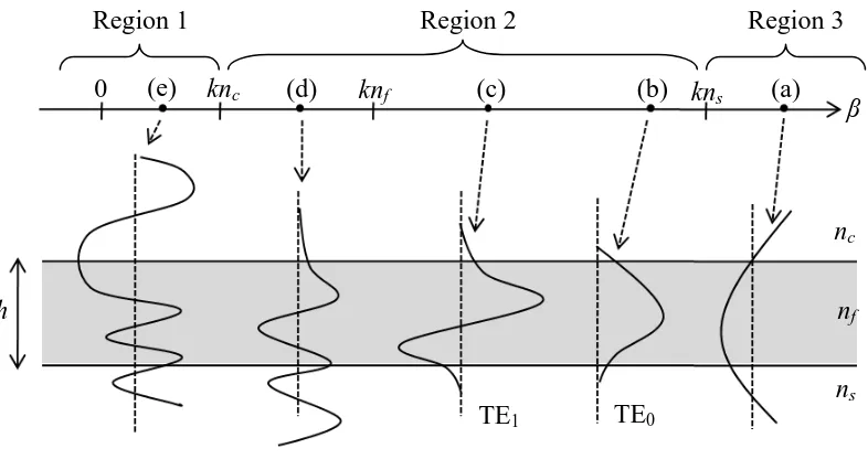
[image:30.595.123.516.505.713.2]E(x,y) is one of the Cartesian component of E(x,y). The solution of Equation 2.5 is either sinusoidal or exponential function of x in each region, depending on whether n -β , i = c, f, s is greater than or less than zero. E(x,y) and ∂E(x,y) /∂x must be continuous at the interface between layers. Now the possible modes will be limited to those shown in Figure 2.2 (Hunsperger, 2002).
Figure 2.2: Modes in planar waveguide (Hunsperger, 2002)
nc
Region 2
Region 1 Region 3
ns
knc (d) knf (c) (a)
0 (e) (b)
β kns
nf
TE0
TE1
h
12 The change in the shape of modes as a function of β at constant frequency ω and nf>ns>nc can be easily seen in Figure 2.2. This is a specific example of
asymmetric waveguide.
If β > kns, the function E(x) must be exponential in all three regions and only
the mode shape (a) shown in Figure 2.2 satisfy the boundary conditions of E(x) and ∂E(x)/ ∂x being continuous at the interface. However, this mode is not really exists as the field increasing unboundedly in layer c and s, implying infinite energy. Modes (b) and (c) are well confined guided zeroth order and first order transverse electric TE0 and TE1 respectively. Such modes can be supported if the value of β lies in the
range between knf and kns. If the value of β is in between knc and kns, a mode shape
like (d) is resulted. This is called substrate mode which confines at upper cladding interface but sinusoidally varying in lower cladding. This mode is not considered as confined mode because it damped after short propagation distance, however found useful in coupling applications. If β is less than knc, the solution of E(x), the modes
are known as radiation mode. Because the energy is radiated easily in upper and lower claddings.
For confined modes that are necessary for effective wave guiding; only discrete values of β are allowed in the range of knf and kns as shown in Equation 2.6;
s (2.6)
These discrete values of β correspond to mode number i.e. zero or fundamental, first and second TE or TM modes (Reed & Knights, 2004) . The numbers of supported modes are dependent on h ω nc, nf and ns . For the case of
asymmetric waveguide where ns<< nc, and fixed h, nc, nf and ns, there is a cutoff
frequency ωc. Below ωc wave guiding will not occur. This ωccorrespond to a long
wavelength λc. All these parameters are related by the equation
n n - n ) λ / n h (2.7)
13
2.1.2 Modes in planar waveguides – ray optic approach
In order to exploit the planar waveguides for sensor applications, the understanding of sensing mechanism is mandatory. Waveguide based sensors usually detect a refractive index change at the core cladding interface. This refractive index change corresponds to a binding event between antigen and antibodies (Zinoviev et al., 2011). The probe used to detect the change in refractive index is “evanescent wave”.
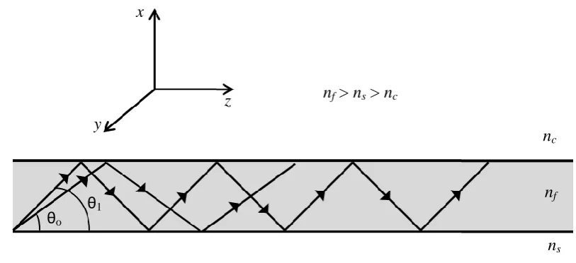
[image:32.595.112.519.412.598.2]While exciting the guided modes of waveguide, the optical confinement is not only within the core but a small portion travels through the interface whose intensity decays exponentially over a hundred of nanometer above the interface. This portion of light is called evanescent wave and it is the back bone of waveguide based biosensors. The ray optical approach explains the light propagation in the waveguide and supports the existence of evanescent field phenomenon. It represents the optical propagation in the form of plane waves that propagates in zig zag manner through x-z plane experience TIR from the interfaces bounding the waveguide as shown in Figure 2.3.
Figure 2.3: Ray-optic representation of optical waveguide
Opposing to physical-optics approach, where plane waves propagating in z direction travel with different phase velocity which is the characteristic of that mode, in ray-optic approach the plane waves posses same physical velocity for each mode but with different angle of reflection from the interfaces. That makes the z component of phase velocity different for each mode (Hunsperger, 2002).
nc
ns
x
z y
nf > ns > nc
θ1
θo
14 Figure 2.3 shows the propagation of two different modes TE0 and TE1 in the form of
ray patterns. The electric, E and magnetic, H fields of these plane waves would add vectorially to give the distribution of E and H comprising the same two modes, propagating in z direction. Both, the ray-optic and physical-optic approaches can be used to represent either TE waves with components Ey, Hz and Hx, or TM waves,
with component Hy, Ez and Ex.
The co-relation between physical-optic and ray-optic approach can be seen by Equation 2.5. The solution of the Equation 2.5 in waveguide i.e. Region 2 represents the form:
) n (2.8)
Where a TE mode is assumed, and p and γ are waveguide structure dependent quantities. Substituting Equation 2.8 into 2.5 for Region 2, the resultant Equation 2.9 is:
β n
(2.9)
As k= ω/v β, p and knf are all propagation constants with units of (m)-1. If a
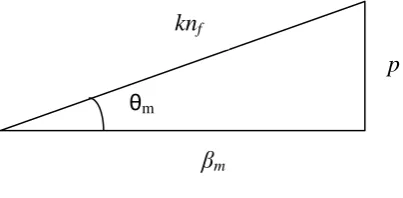
plane wave travelling at an angle m a β ) with respect to z- direction and
having propagation constant kn2, its mode can be represented by z-direction
propagation constant βm and x-direction propagation constant p. as shown in Figure
[image:33.595.217.419.576.675.2]2.4.
Figure 2.4: Geometrical relationships of optical waveguide propagation constants p
βm
knf
15 As the frequency is constant, k nf = ω/ v nf is also a constant quantity, while rest of
parameters such as ,βm and pare associated with mth mode and these parameters
are different for different modes.
[image:34.595.119.527.218.314.2]The simplicity of ray-optic model lies in the only requirement of nell’s law with TIR phenomenon. Consider a ray of light propagating in a three layer structure as shown in Figure 2.5 (Hunsperger, 2002).
Figure 2.5: Ray-optic approach for (a) air radiation mode, (b) substrate radiation mode, (c) guided mode
The light rays of Figure 2.5(a), (b) and (c) corresponds to air radiation, substrate radiation and a guided mode, respectively. The angle of reflection and refraction φi, i=c, f, s are measured with respect to the normal to the interface planes.
From nell’s law,
n φ / n φ n / n (2.10)
And,
n φ / n φ n /n (2.11)
When φsis very small, light ray experience only the refraction and freely pass
through interfaces as shown in Figure 2.5(a) and it is the radiation mode of waveguide. As φs increases until where φf exceeds the critical angle for TIR at nf -nc
interface, the light is partially confined and this corresponds to the substrate mode as shown in Figure 2.5(b). The condition for TIR is given in Equation 2.12 as:
(2.12)
Or, combining (2.12) with (2.11)
nc nc nc
nf nf
nf
ns ns ns
φs φs φs
φf φf φf φf φf
φf
16
(2.13)
As φs is further increased φf also exceeds the critical angle at nf-ns interface,
the light wave becomes confine as shown in Figure 2.5(c) that correspond to a guided mode. In this case the critical angle is given by Equation 2.14, i.e.
(2.14)
Or, combining (2.14) with (2.11)
) (2.15)
The Equations 2.12 and 2.14 determine the conditions for the modes supported by a waveguide as a function of φf which are equivalent to the conditions
in physical optic approach as a function of β.
From Figure 2.5, it is clear that φf relates β by,
(2.16)
Thus, results obtained to determine the mode supported by waveguide structure by physical-optic approach are merely a repeat of ray-optic approach conditions.
The wave front of plane waves that are normal to the zig zag rays are assumed to be infinite which require a constant phase over the plane. Thus there is much overlapping of the wave as they travel in zig-zag path. In order to preservation of a wave across the waveguide the total phase change from a point on a wave front that travels from nf -ns interface to the nf -nc interface and back again must be the a
multiple of 2π. This leads to the condition:
17 Where h is the thickness of waveguide region 2, is the angle of reflection with respect to z direction, m is mode number and
φ
fs andφ
fc are the phase changes sufferupon TIR phenomenon.
The phases , represent Goos-Hänchen shifts. These phase
shifts are interpreted as penetration of electric field in substrate and cover region of waveguide which is also called “Evanescent Wave”.
2.2 Propagation loss in waveguides
An effective planar waveguide is the one that completely transfer the input optical signal to the desired distance. However it is not possible to achieve 100% efficiency due to factors contributing the propagation losses. The losses in optical propagation depend on the properties of the deposited film. A careful characterization after fabrication of each layer could help to achieve the optimized deposition parameters. This, in turn, lowers the propagation losses. There are several types of propagation losses. These include scattering losses, radiation losses, absorption losses and polarization dependent losses (Tamir, 1988).
There are two types of scattering losses observed in planar waveguides i.e. volume scattering losses and surface scattering losses. Volume scattering losses are caused by the imperfections such as voids, crystalline defects and contaminant atoms within the waveguides (Reed & Knights, 2004). The loss per unit length due to volume scattering is proportional to the number of imperfections per unit length. Volume scattering loss very strongly depends on the relative size of imperfections as compared to the wavelength of light in material.
Surface scattering loss appears when the light interacts with each interface in planar waveguide several time and even slightly rough surfaces could cause the attenuation of light. The effect is greater for longer length of waveguides or higher modes. In a planar waveguide of length L as shown in Figure 2.6, the number of reflections from each surface is given by Equation 2.18,
18 Since m is larger for the higher order modes, it causes the rises the number of
[image:37.595.116.527.134.278.2]reflection from each interface (Hunsperger, 2002).
Figure 2.6: An approach to determine scattering loss in planar waveguide Roughness at waveguide boundaries which is known as interface roughness, can lead to scattering losses. It is a type of scattering loss which is generally higher at boundaries where the refractive index change is large (Tamir, 1988). The theory for approximating the scattering through the interface of optical waveguide was first introduced by Tien in 1971 (Tien, 1971). This theory was based upon the specular reflection of power from a surface. If the incident beam has power Pi, the specular reflected power, Pr from a surface is given by ((Hunsperger, 2002).
exp - π nλ
o cos
2
(2.19)
According to Equation 2.19, is the variance of surface roughness, that is, root mean square roughness, m is propagation angle within the waveguide and nf is
the refractive index of core. By considering, the total power flow in a given waveguide, together with the loss at both waveguide interface based upon Equation 2.19, Tien (Tien, 1971) produced following expression for the loss co-efficient due to interface scattering.
s 2 sin cos π n c 2
s2)1/2 λo
2
s
(2.20)
m
ns
nf
nc
h
L
x
19 In Equation 2.20, c and s are the root mean square rough nesses of upper and lower
waveguide interfaces respectively, kyc and kylare the y-directed decay constants in
upper and lower cladding layers respectively and h is the thickness of waveguide. Equation 2.20 points the requirement of low interface roughness in the waveguide. Low interface roughness leads to reduce the scattering losses.
Substrate radiation losses affect the light propagation due to leakage of light towards substrates due to having high refractive index as compare to core layer. The prevention is possible by depositing a thick lower cladding layer with respect to the thickness of core layer. Experimental studies show that for a 100 nm thickness of core layer , 1 µm thick lower cladding is enough to prevent optical leakage if the refractive index contrast is higher such as Δn ~ 0.5 (Heideman et al., 1991).
Absorption losses in silicon nitride based planar waveguides by sputtering technique contribute to silicon dangling bonds as reported by Jessica Sandland (Sandland, 2004). Silicon is good absorber of visible region therefore becomes a high demand material for optical detector and solar panels.
2.3 Waveguide fabrication by sputtering technique
Sputtering technique is a physical vapour deposition process and widely accepted for the thin film deposition (Wasa, Kitabatake, & Adachi, 2004). The need for alloys with stringent stoichiometric limits, conformal coverage, and better adherence, for magnetic and microelectronic materials, increased the demand for sputtering deposition. Today, the capabilities of sputtering and the availability of high- purity targets and various gases make sputtering technique a popular choice for the deposition of thin films (Ohring, 2001). Some of the benefits of sputtering include:
(i) High uniformity of thickness (ii) Good adhesion of film to substrate (iii) Reproducibility of films
(iv) Ability to deposit and maintain the stoichiometry of the target material (v) Relative simplicity of thickness control
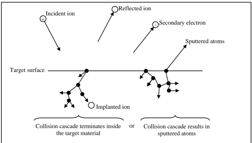
20 The addition of RF (which allows the sputtering of insulators) and magnetron extended the capability of sputtering. This is a momentum transfer process in which a solid material source (target) is bombarded with ions to eject the material atoms (Sarakinos, Alami, & Konstantinidis, 2010). These atoms then travel through the substrate and settled to form thin film. The graphical representation of ion-target surface interaction is shown in Figure 2.7 (Ohring, 2001).
Figure 2.7: Interactions of ion with target surface (Ohring, 2001)
According to Figure 2.7 an ion impinges the target surface, several phenomenons may occur:
The ion doesn’t have sufficient energy, it may reflect back from target surface.
The impact of ion causes to eject the secondary electron from the target.
The ion implants in the target.
The ion impact rearrange the structure in the target material which disturb the stochiometry of target.
The ion impact ejects the target material atoms by setting a series of collisions between target material and bombarding ions. This ejection process is called sputtering.
Reflected ion Incident ion
Secondary electron
Sputtered atoms
Target surface +
-
Implanted ion
Collision cascade terminates inside the target material
21 Therefore it is observed that the sufficient supply of ions is required to continue the sputtering process. The sputtering gas enters in the sputtering chamber in form of gas molecules and an external supply of electrons is provided to ionize the gas molecules.
2.3.1 Sputtering process considerations
2.3.1.1 Sputtering yield
The sputter yield S is defined as mean number of atoms removed from the sputtering target per incident ion (Wasa et al., 2004) and is given by
S atoms removed
incident ions (2.21)
Mathematically,
π 2
M1M2 (M1 M2)
E1
Eb (2.22)
In Equation (2.22), M1 and M2 are the masses of incident ion and target atom
respectively. E1 is the incident ion energy, Eb is the surface binding energy of target
material, and is a measure of efficiency of momentum transfer. Equation 2.22 is the theoretical modeling of linear collision cascade regime which happens as a result of ion impact. The result of this regime is sputtering, that is, the ejection of target atoms. This theoretical modeling was presented by Sigmund and it provides the specific dependence of sputtering yield (S) on the energy (E1) of incident ion. This
22
2.3.1.2 Mean free path
Mean free path of an atom λmfp, is define as the path for which an atom travel without
any collision. Any collision with other atoms or incident ion could re-track it to directions other than substrate.
Mathematically,
mfp
RT) (2.23)
R is ideal gas constant, dc is collision diameter and P is the pressure during
deposition. At lower sputtering pressure and assuming the collision diameter in angstroms, the mean free path of an atom is very large compare to deposition chamber. Sandland (Sandland, 2004) suggests that there is no collision before arrival at substrate. However, this also suggests that higher the pressure could lower the mean free path which could result in scattering of atom during its travel. This proves the existence of an optimum value of sputtering pressure beyond which the deposition rate reduced after reaching the maximum due to back scattering of sputtered atoms in plasma.
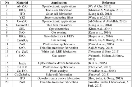
2.3.2 Applications of sputtering technique
23 Table 2.1: Applications of DC sputtering technique
No Material Application Reference
1 InGaZnO4 Thin film transistors fabrication (Raja et al., 2013)
2 ZnCdO Fabrication of optoelectronic devices for
blue/UV region (Shtepliuk et al., 2013)
3 ZnO Semiconductor devices fabrication (Vijayalakshmi et al., 2013)
4 a-IGZO Thin film transistors fabrication (Yasuno et al., 2013)
5 Cu3N Optical storage devices (Bai et al., 2013)
6 TiO2 photocatalyst material (Wang et al., 2014)
7 -Fe2O3 photoelectrochemical application (Huang et al., 2014)
8 TiSiN Self lubrication films in tool cutting (Fernandes et al., 2014)
9 NiO–Ag Gas sensing (Reddy, Reddy, & Reddy, 2014)
10 C-TiN Biomaterial (Sedira et al., 2014)
11 V2O5 Infra red detectors (Raj, Gupta, & Sridharan, 2015)
12
Ni-HfOx-Pt Random access memory fabrication (Ito et al., 2015)
13 IZO Transparent electrode in Solar cell (Werner et al., 2015)
14 Ti TiO2 nanotubes (Chappanda et al., 2015)
15 Al and
Mg Plasmonics structure fabrication (Appusamy et al., 2015)
16 AlN Sensing applications (Smecca et al., 2015)
17 AlN High-frequency surface acoustic wave
devices fabrication (Ke et al., 2015)
18 ZnO:Al Optoelectronic devices fabrication (Qu et al., 2015)
19 Fe-WO3 Gas sensing applications (Tesfamichael et al., 2015)
20 HfN Protective coatings (García-González et al., 2015)
Table 2.2: Applications of RF sputtering technique
No Material Application Reference
1 Al- ZnO Optoelectronic applications (Wu & Chu, 2013)
2 HfO2 Transistor fabrication (Khairnar & Mahajan, 2013)
3 ITO Solar cell fabrication (Liang & Qi, 2013)
4 YSZ Super conducting films (Wang et al.,2013)
5 Co-ZnO Optoelectronic applications (Al-Salman & Abdullah, 2013)
6 GaSnZnO Thin film transistors (Liang et al., 2014)
7 SiNx Optoelectronics (Kitao et al., 2014)
8 SnO2 Gas sensing (Kaur et al., 2014)
9 HfO2 Gate dielectrics in FETs (Haque et al., 2014)
10 CuAlO2 Gas sensing (Hsieh, Lu, & Hwang, 2014)
11 ZnO Photovoltaic applications (Purohit et al., 2015)
12 SnO2 Thin film transistor fabrication (Saji & Mary, 2015)
13 Cu–GaN White light LED fabrication (Yohannes & Kuo, 2015)
14 SnO2 Gas sensor (Velmathi, Mohan, & Henry,
2015)
15 In2S3 Optoelectronic device fabrication (Ji et al., 2015)
16 BiFeO3 Photovoltaic applications (Chen et al., 2015)
17 Cu-TiO2 Photo catalyst (Sreedhar et al., 2015)
18 Cu2ZnSnSe4 Solar cell fabrication (Fan et al., 2015)
19 ITO Optoelectronics device fabrication (Heo, Sohn, & Gwag, 2015) 20 ZnO Thin film transistor fabrication (Amutha Surabi, Chandradass, &
[image:42.595.108.531.108.410.2] [image:42.595.106.532.457.736.2]24
2.4 Effect of sputtering parameters on thin film properties
2.4.1 Effect of sputtering power
The sputtering power is a very common parameter to control the properties of thin films. Based on application, the sputtering power can be increase or decrease to get the required properties. Zeng et al. (2011) investigated this parameter for the deposition of (Cd1-x Znx)Te thin films on glass substrates. The power was varied from
60- 120 W during the deposition. The growth rate and crystallanity was found to improve linearly with the applied sputtering power.
Indium Gallium Zinc Oxide (In-Ga-ZnO) thin films were deposited at sputtering powers from 200 W to 500 W by Li et al. (2012). The results reported the increase in growth rate, optical band gap and carrier mobility with increase in power. Yu et al. (2012) deposited the Cu(In1-x Gax) Se2 thin films on glass substrates at
various sputtering power ranging from 50 W to 150 W. The observation on crystallinity and growth rate found these properties have a linear relationship with sputtering power.
Tseng and colleagues studied the effect of power on the deposition of AZO thin films (Tseng et al., 2012). The deposition was carried out on glass substrate and sputtering power was varied from 20 W to 150 W. The result shows an increase in growth rate with the increase in power. Similar behavior was observed for grain size and surface roughness. The variation in power affects the stochiometry by changing the aluminum concentration linearly. The resistivity of films decreased with increase in sputtering power.
REFERENCES
Abdel-Hady, K., Hesham, M. A. S., Marwa, N., & Ahmed, A. B. (2013). Fabrication of Congo Red/Oxidized Porous Silicon (CR/OPS) pH-Sensors. Materials Sciences and Applications, 04(08), 9.
Abolmasov, S. N. (2012). Physics and engineering of crossed-field discharge devices. Plasma Sources Science and Technology, 21(3), 035006.
Al-Lawati, Z. H., Bushby, R. J., & Evans, S. D. (2013). Alignment of a columnar hexagonal discotic liquid crystal on self-assembled monolayers. The Journal of Physical Chemistry C, 117(15), 7533-7539.
Al-Salman, H. S., & Abdullah, M. J. (2013). Fabrication and Characterization of Undoped and Cobalt-doped ZnO Based UV Photodetector Prepared by RF-sputtering. Journal of Materials Science & Technology, 29(12), 1139-1145. Ali, K., Khan, S. A., & MatJafri, M. Z. (2015). Low temperature nanocrystalline
silicon nitride film grown on silicon (111) by radio frequency sputtering system. Optik-International Journal for Light and Electron Optics, 126(6), 596-598.
Amirshaqaqi, N., Salami-Kalajahi, M., & Mahdavian, M. (2014). Investigation of corrosion behavior of aluminum flakes coated by polymeric nanolayer: effect of polymer type. Corrosion Science, 87, 392-396.
Amutha Surabi, M., Chandradass, J., & Park, S.-J. (2015). ZnO-Based Thin Film Transistor Fabricated Using Radio Frequency Magnetron Sputtering at Low Temperature. Materials and Manufacturing Processes, 30(2), 175-178. Appusamy, K., Jiao, X., Blair, S., Nahata, A., & Guruswamy, S. (2015). Mg thin
films with Al seed layers for UV plasmonics. Journal of Physics D: Applied Physics, 48(18), 184009.
-111 Nb2O5 glass ceramic planar waveguides for photonic applications. Optical
Materials, 35(3), 387-396.
Bai, Q., Yang, J., Li, Y., Wang, L., Wang, H., Ren, S., Liu, S. and Huang, W. (2013). Effect of N2-gas flow rates on the structures and properties of copper nitride
films prepared by reactive DC magnetron sputtering. Vacuum, 89, 78-81. Bao, X., Sun, L., Shen, W., Yang, C., Chen, W., & Yang, R. (2014). Facile
preparation of TiOX film as an interface material for efficient inverted
polymer solar cells. Journal of Materials Chemistry A, 2(6), 1732-1737. Barattin, R., & Voyer, N. (2008). Chemical modifications of AFM tips for the study
of molecular recognition events. Chemical Communications, (13), 1513-1532.
Bauters, J. F., Heck, M. J. R., John, D. D., Barton, J. S., Bruinink, C. M., Leinse, A., Heideman, R.G., Blumenthal, D.J. & Bowers, J.E. (2011). Planar waveguides with less than 0.1 dB/m propagation loss fabricated with wafer bonding. Optics express, 19(24), 24090-24101.
Ben-Awuah, J., & Eswaran, P. (2015). Effect of bioturbation on reservoir rock quality of sandstones: A case from the Baram Delta, offshore Sarawak, Malaysia. Petroleum Exploration and Development, 42(2), 223-231.
Benmore, C. J., R Weber, J. K., Tailor, A. N., Cherry, B. R., Yarger, J. L., Mou, Q., Weber, W., Neuefeind, J. & Byrn, S.R. (2013). Structural characterization and aging of glassy pharmaceuticals made using acoustic levitation. Journal of pharmaceutical sciences, 102(4), 1290-1300.
Bradley, J. D. B., Evans, C. C., Parsy, F., Phillips, K. C., Senaratne, R., Marti, E. & Mazur, E. (2010). Low-loss TiO2 planar waveguides for nanophotonic
applications. Paper presented at the 23rd Annual Meeting of the IEEE Photonics Society.
Campoy-Quiles, M., Alonso, M. I., Bradley, D. D. C., & Richter, L. J. (2014). Advanced ellipsometric characterization of conjugated polymer films. Advanced Functional Materials, 24(15), 2116-2134.
112 Chaoumead, A., Sung, Y.M., & Kwak, D.J. (2012). The effects of RF sputtering power and gas pressure on structural and electrical properties of ITiO thin film. Advances in Condensed Matter Physics, 2012, 1-7.
Chapman, B. N. (1980). Glow Discharge Processes: Sputtering and Plasma Etching: WILEY.
Chappanda, K. N., Smith, Y. R., Rieth, L. W., Tathireddy, P., Misra, M., & Mohanty, S. K. (2015). Effect of Sputtering Parameters on the Morphology of TiO 2 Nanotubes Synthesized From Thin Ti Film on Si Substrate. Nanotechnology, IEEE Transactions on, 14(1), 18-25.
Chen, M., Ding, J., Qiu, J., & Yuan, N. (2015). Effect of film thickness and bottom electrode material on the ferroelectric and photovoltaic properties of sputtered polycrystalline BiFeO3 films. Materials Letters, 139, 325-328.
Choo, S. J., Kim, J., Lee, K. W., Lee, D. H., Shin, H.J., & Park, J. H. (2014). An integrated Mach-Zehnder interferometric biosensor with a silicon oxynitride waveguide by plasma-enhanced chemical vapor deposition. Current Applied Physics, 14(7), 954-959.
Craig, M., Holmberg, K., Le Ru, E., & Etchegoin, P. (2014). Polypeptide multilayer self-assembly studied by ellipsometry. Journal of drug delivery, 2014, 1-5. Cui, L., Wang, G. G., Zhang, H. Y., Sun, R., Kuang, X. P., & Han, J. C. (2013).
Effect of film thickness and annealing temperature on the structural and optical properties of ZnO thin films deposited on sapphire (0001) substrates by sol–gel. Ceramics International, 39(3), 3261-3268.
de Castro, M. S. B., Ferreira, C. L., & de Avillez, R. R. (2013). Vanadium oxide thin films produced by magnetron sputtering from a V2O5 target at room
temperature. Infrared Physics & Technology, 60, 103-107.
Duval, D., Gonzalez-Guerrero, A. B., Dante, S., Osmond, J., Monge, R., Fernandez, L. J., Zinoviev, K.E., Domínguez, C. & Lechuga, L.M. (2012). Nanophotonic lab-on-a-chip platforms including novel bimodal interferometers, microfluidics and grating couplers. Lab on a Chip, 12(11), 1987-1994.
113 Fan, P., Zhao, J., Liang, G.X., Gu, D., Zheng, Z.H., Zhang, D.P., Cai, X.M., Luo, J.T. & Ye, F. (2015). Effects of annealing treatment on the properties of CZTSe thin films deposited by RF-magnetron sputtering. Journal of Alloys and Compounds, 625, 171-174.
Fernandes, F., Loureiro, A., Polcar, T., & Cavaleiro, A. (2014). The effect of increasing V content on the structure, mechanical properties and oxidation resistance of Ti-Si-V-N films deposited by DC reactive magnetron sputtering. Applied Surface Science, 289, 114-123.
Fultz, B., & Howe, J. M. (2012). Transmission electron microscopy and diffractometry of materials: Springer Science & Business Media.
García-González, L., Zamora-Peredo, L., Flores-Ramírez, N., Garnica-Romo, M. G., & Hernández-Torres, J. (2015). Influence of Nitrogen Flow Rates on the Structure, Hardness, and Electrical Resistivity of HfN Coatings by DC Sputtering. Journal of Materials Engineering and Performance, 24(4), 1558-1564.
Giacon, V. M., da Silva Padilha, G., & Bartoli, J. R. (2015). Fabrication and characterization of polymeric optical by plasma fluorination process. Optik-International Journal for Light and Electron Optics, 126(1), 74-76.
Haag, F., Beitelschmidt, D., Eckert, J. r., & Durst, K. (2014). Influences of residual stresses on the serrated flow in bulk metallic glass under elastostatic four-point bending-A nanoindentation and atomic force microscopy study. Acta Materialia, 70, 188-197.
Habibi, M. H., & Karimi, B. (2014). Application of impregnation combustion method for fabrication of nanostructure CuO/ZnO composite oxide: XRD, FESEM, DRS and FTIR study. Journal of Industrial and Engineering Chemistry, 20(4), 1566-1570.
Hampshire, S. (2007). Silicon nitride ceramics–review of structure, processing and properties. Journal of Achievements in Materials and Manufacturing Engineering, 24(1), 43-50.
Haque, S. M., Sagdeo, P. R., Balaji, S., Sridhar, K., Kumar, S., Bhattacharyya, D., Bhattacharyya, D. & Sahoo, N.K. (2014). Effect of substrate bias and oxygen partial pressure on properties of RF magnetron sputtered HfO2 thin films.
114 Harata, T., Aono, M., Kitazawa, N., & Watanabe, Y. (2014). Correlation of photothermal conversion on the photo-induced deformation of amorphous carbon nitride films prepared by reactive sputtering. Applied Physics Letters, 105(5), 051905.
Heideman, R. G., Kooyman, R. P. H., & Greve, J. (1991). Development of an optical waveguide interferometric immunosensor. Sensors and Actuators B: Chemical, 4(3), 297-299.
Heo, K. C., Sohn, Y., & Gwag, J. S. (2015). Effects of an additional magnetic field in ITO thin film deposition by magnetron sputtering. Ceramics International, 41(1), 617-621.
Hirohata, Y., Shimamoto, N., Hino, T., Yamashima, T., & Yabe, K. (1994). Properties of silicon nitride films prepared by magnetron sputtering. Thin Solid Films, 253(1-2), 425-429.
Hsieh, P.H., Lu, Y.M., & Hwang, W.S. (2014). Effects of RF power on the growth behaviors of CuAlO2 thin films. Ceramics International, 40(7), 9361-9366.
Huang, M.C., Wang,T., Wu, C.C., Chang, W.S., Lin, J.C., & Yen, T.H. (2014). The optical, structural and photoelectrochemical characteristics of porous hematite hollow spheres prepared by DC magnetron sputtering process via polystyrene spheres template. Ceramics International, 40(7), 10537-10544.
Hunsperger, R. G. (2002). Integrated optics: theory and technology: Springer Science & Business Media.
Ito, D., Hamada, Y., Otsuka, S., Shimizu, T., & Shingubara, S. (2015). Oxide thickness dependence of resistive switching characteristics for Ni/HfOx/Pt resistive random access memory device. Japanese Journal of Applied Physics, 54(6S1), 06FH11.
Jeong, S. H., & Boo, J. H. (2004). Influence of target-to-substrate distance on the properties of AZO films grown by RF magnetron sputtering. Thin Solid Films, 447, 105-110.
Ji, Y., Ou, Y., Yu, Z., Yan, Y., Wang, D., Yan, C., Liu, L., Zhang, Y. & Zhao, Y. (2015). Effect of film thickness on physical properties of RF sputtered In2S3
layers. Surface and Coatings Technology, 276, 587-594.