A Compact Switchable and Tunable Bandpass Filter
Muhammad F. Karim* and Mohammed Y. Siyal
Abstract—In this paper, an integrated switchable and tunable bandpass filter is designed, simulated, and fabricated. This integrated bandpass filter is able to switch as well as tune in the ultra-wideband (UWB) as well as 2.4 GHz band. At first, a UWB bandpass filter is developed which consists of two bent shorted quarter-wavelength stubs and a connecting half-wavelength stub. Subsequently, a 2.4 GHz bandpass filter is realized by connecting another half-wavelength stub on top of the UWB filter. RF pin-diodes are used for switching the bands between UWB and 2.4 GHz bandpass filter. The switchable bandpass filter converts into a tunable filter by changing the inductance or the length of shorted stubs through the pin diodes. A detailed parametric analysis is done for calculating different stubs lengths of the UWB as well 2.4 GHz bandpass filter. The simulation results show a high rejection level of >40 dB at the lower frequency and a low insertion loss of 0.8 dB in the passband for UWB filter. For 2.4 GHz bandpass filter, the simulation results show an insertion loss of 0.42 dB and a 3 dB bandwidth of 796 MHz. The filter is fabricated on a Rogers 4003 substrate, and the measurement results of the switchable filter in the UWB band show an insertion loss of 2.1 dB and a 3 dB bandwidth of 7 GHz. In the case of 2.4 GHz bandpass filter, the insertion loss is 0.78 dB.
1. INTRODUCTION
Recent development in wireless communications systems demands radio frequency (RF) devices to operate in multiple and separated frequency bands. As such, a single filter cannot fulfill filtering requirements for receivers operating in the UWB and wireless local area network (WLAN) bands simultaneously. In addition, the use of multiple filters occupies a large surface area [1]. Tunable and switchable microwave circuits have allowed increased system functionality with lower weight and cost than existing systems. Therefore, switchable and tunable filters are of great interest [2, 3]. Tunable filters have been demonstrated with the use of semiconductor varactor diodes [4–6] and micro-electromechanical systems (MEMS) [7–10]. For frequencies below 10 GHz, PIN diodes and varactor diodes are able to demonstrate Q > 50 with reduced cost, easier packaging, and lower bias voltage. Significant research activities have been carried out to explore various UWB filters for indoor and handheld systems. Various UWB bandpass filters have been developed to achieve a fractional bandwidth of 110% at the central frequency of 6.85 GHz [11, 12]. Meanwhile, IEEE 802.11b/g WLAN standard at 2.4 GHz band has also been extensively incorporated into mobile and handheld devices, such as laptop, cell-phones, and PDAs. Bandpass filters operating at 2.4 GHz have been developed over the years with various configurations [13, 14].
The resonant frequency and coupling between resonators and input/output coupling were adjusted using MEMS switches in edge coupled filter topologies that was implemented in [15]. The filter response shows three distinct states at 8, 9, and 10 GHz, and preserves constant bandwidth over the switchable range [15]. Another switchable filter topology was demonstrated, which included two folded
Received 18 July 2019, Accepted 26 August 2019, Scheduled 14 September 2019
* Corresponding author: Muhammad Faeyz Karim ([email protected]).
resonator extensions switched by PIN diodes. It was able to switch between WiFi and universal mobile telecommunications (UMTS) transmit band standards [16]. A bandstop filter with the topology can be conveniently switched to have a bandpass response due to the presence of the inter-resonator coupling structures and has recently been reported. The filter was reconfigured by a pair of reflective MEMS switches, and it was demonstrated that the switchable filter can exhibit both bandstop and bandpass filter responses [17]. An integrated filter that is able to switch as well as tune has not been reported in literature.
In this paper, an integrated new switchable and tunable bandpass filter is presented. The proposed filter is able to switch and tune in the UWB and 2.4 GHz band. At first, a UWB bandpass filter consisting of two bent shorted quarter-wavelength stubs and a connecting half-wavelength stub is developed. It switches from UWB to 2.4 GHz bandpass filter by connecting another half-wavelength stub through RF pin diodes. Using pin diodes, the switchable filter becomes a tunable bandpass filter by changing the inductance or the length of the shorted stubs. The switchable and tunable bandpass filter has the merit of compact size and low insertion loss.
2. DESIGN OF SWITCHABLE AND TUNABLE BANDPASS FILTER 2.1. Design of Switchable Bandpass Filter
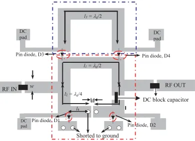
Figure 1 shows the schematic of a switchable and tunable bandpass filter. The UWB bandpass filter consisting of two bent short stubs l2 of quarter wavelength and one bent connecting line in the form of a square loop. Unlike the conventional quarter-wave filter, the connecting line between the two shorted stubs has a length of half wavelength, l1, in order to obtain a wider bandwidth. The bending of the stubs also makes the design more compact than the conventional structure. The UWB bandpass filter is designed with the center frequency at 6.85 GHz and the lengths of stubsl1 = 12.4 mm andl2 = 6.2 mm, respectively. The gap between the folded stubs isg= 0.3 mm, and this helps in the optimization of the bandpass frequency characteristics. Figure 2 shows the simulation results for the UWB bandpass filter
l3 = λg/2
Shorted to ground DC
pad
g
Pin diode, D3 Pin diode, D4
RF IN RF OUT
Pin diode, D1
Pin diode, D2 l1 = λg/2
l2 = λg/4
w
DC pad
DC pad
l4
DC block capacitor
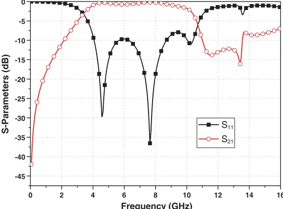
0 2 4 6 8 10 12 14 16 -45 -40 -35 -30 -25 -20 -15 -10 -5 0 S-Parameters (dB) Frequency (GHz) S11 S21
Figure 2. Simulation results of the UWB switchable bandpass filter.
using the commercial software IE3D. It shows a high rejection level of >40 dB at the lower frequency and a low insertion loss of 0.8 dB in the passband.
The bandwidth of the UWB filter within the lower dotted red grid in Figure 1 depends on the centre connecting line l1 as discussed previously. Using ABCD parameters, an expression can be obtained:
A B C D = 1 0 Y 1
cosβl1 jZ0sinβl1 jY0sinβl1 cosβl1
1 0
Y 1
(1)
S21 =
2
2 cosβl1−2jY Z0sinβl1+ 2Y Y0cosβl1−jY02sinβl1−jY sinβl1−jsinβl1 (2)
Y = −jY0cotβl2 (3)
where Y is the admittance, and Zo is the characteristics impedance. Eq. (3) is useful for determining
0 1 2 3 4 5 6 7 8 9 10
-50 -45 -40 -35 -30 -25 -20 -15 -10 -5 0 S-Parameters (dB) Frequency (GHz) S11 S21
the bandwidth of the UWB bandpass filter.
When a stub of lengthl3 =λg/2 is inserted into the filter as shown in the upper dotted blue grid in Figure 1, it becomes a switchable bandpass filter. It switches the band from UWB to 2.4 GHz band as shown in Figure 3. The insertion loss is 0.42 dB with a 3-dB bandwidth of 796 MHz. The out of band rejection is more than 4 dB on the lower and upper side bands of 2.4 GHz filter. The RF pin diodes D3 and D4 are placed to realize the switchable characteristics as depicted in Figure 1.
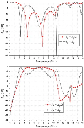
2.1.1. Varying the Length of Stub, l1, of UWB Bandpass Filter
In this case, suppose that the length of the stub, l1, of UWB bandpass filter changes from λg/2 to λg with other two lengths l2 and l3 fixed at λg/4 and λg/2. As depicted in Figure 4, the insertion loss for l1 = λg is quite high in the range of 4 dB with ripples appearing in the passband. With length l1 = λg/2, the insertion loss is less than 1 dB, and it satisfies the requirement of the UWB band in terms of bandwidth.
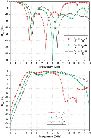
2.1.2. Varying the Length of Stub, l2, of UWB Bandpass Filter
A parametric study is done by varying the length of the stubs,l2, for UWB bandpass filter. The other two lengths l1 and l3 are fixed at λg/2 and λg/2, respectively. The variation in the lengths also shows the tunability characteristics of around 600 MHz as shown in Figure 5. The results also show that for l2 = λg/6 a high insertion loss is about 2 dB at 7 GHz. The 3-dB bandwidth is 9.8 GHz and is out of UWB. The return loss also decreases below 10 dB from 6 to 8 GHz. The length l2 = λg/2 shows the minimum insertion loss of less than 1 dB and covers the UWB. The out of band rejection is more than 40 dB at lower frequency band and over 15 dB at higher band. Subsequentlyl2 =λg/8 in Figure 5 shows the worst insertion loss of 3 dB at 7.2 GHz among the three, and the return loss drops below 10 dB from 6 to 9 GHz.
2.2. Design of Tunable Bandpass Filter
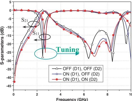
The tunable bandpass filter is developed by changing the length of the stub,l2. The detailed analysis on the variation of the length is presented in the next subsection. Pin-diodes D1, D2, D3, and D4 are incorporated and turn ON or OFF simultaneously for tunability as shown in Figure 1. When diodes D3 and D4 are turned OFF and diodes D1 and D2 turned ON, the filter shows UWB characteristics as shown in Figure 6. This is because the inductance or the length of the stub changes. Similarly, when diodes D3 and D4 are turned ON and D1 and D2 turned ON and OFF respectively, it behaves as a tunable filter in the 2.4 GHz band as shown in Figure 7.
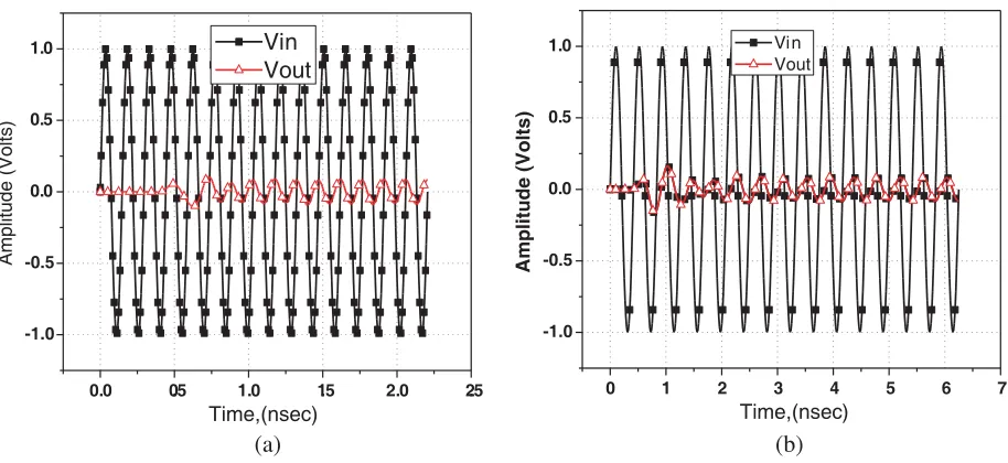
A transient response of the switchable filter at the UWB and 2.4 GHz band is also calculated using the Agilent ADS transient simulator controller in the co-simulation environment. The delay of the filter
0 2 4 6 8 10 12 14 16
-45 -40 -35 -30 -25 -20 -15 -10 -5 0 5
OFF (D1), OFF (D2) ON (D1), OFF (D2) ON (D1), ON (D2)
S-parameters (dB)
Frequency (GHz)
Tuning
S
11S
21Figure 6. Simulation results of the tunable UWB bandpass filter.
0 2 4 6 8 10
-45 -40 -35 -30 -25 -20 -15 -10 -5 0 5 S-parameters (dB) Frequency (GHz)
OFF (D1), OFF (D2) ON (D1), OFF (D2) ON (D1), ON (D2)
Tuning
S11 S21
0.0 0.5 1.0 1.5 2.0 2.5 -1.0
-0.5 0.0 0.5
1.0 Vin
Vout
Amplitude (Volts)
Time,(nsec)
0 1 2 3 4 5 6 7
-1.0 -0.5 0.0 0.5 1.0
Amplitude (Volts)
Time,(nsec)
Vin Vout
(a) (b)
Figure 8. Transient responses of the filter (a) UWB and (b) 2.4 GHz filter.
is calculated and compared between the input voltage peak, Vin, and output voltage peak, Vout. The delay through the switchable filter in the UWB is 34 ps as shown in Figure 8(a). For 2.4 GHz band, it is 320 ps as shown in Figure 8(b).
2.2.1. Varying the Length of the Stub, l2, of 2.4 GHz Bandpass Filter
Figure 9. Simulation result for the variation in the length of stub,l2, of 2.4 GHz bandpass filter.
2.2.2. Varying the Length of the Stub, l3 of 2.4 GHz Bandpass Filter
The final parametric study is for the length l3 of 2.4 GHz bandpass filter. The lengths l1 and l2 are fixed atλg/2 andλg/4, respectively. The observation in this case is that there is a wide frequency shift if the lengths are changed fromλg, λg/2 toλg/4. The shift in the frequency is more than 66% as the results in Figure 10. The rejection of l3 =λg stub length is very poor at the higher frequency band. However, the configuration l3=λg is not realizable with the RF pin diodes.
3. EXPERIMENTAL RESULTS AND DISCUSSIONS
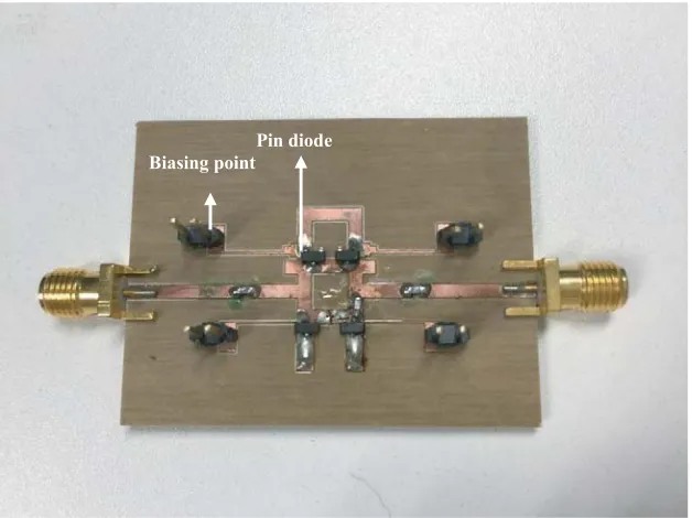
The switchable and tunable filter is fabricated on a Rogers substrate with dielectric constant,εr= 3.38,
Figure 10. Simulation result for the variation in the length of stub, l3, of 2.4 GHz bandpass filter.
Pin diode Biasing point
Figure 11. Fabricated structure — The switchable and tunable filter.
0 2 4 6 8 10 12 14 16 -60 -50 -40 -30 -20 -10 0
OFF (D1), OFF (D2) ON (D1), OFF (D2) ON (D1), ON (D2)
S-parameters (dB) Frequency (GHz) S11 S21
Tuning
9 10 -60 -50 -40 -30 -20 -10 0OFF (D1), OFF (D2) ON (D1), OFF (D2) ON (D1), ON (D2)
S-parameters (dB)
Frequency (GHz) S11
S21
1.0 1.5 2.0 2.5 3.0 3.5 4.0 -30 -25 -20 -15 -10 -5 0 S-parameters (dB) Frequency (GHz)
Tuning
0 1 2 3 4 5 6 7 8
(a) (b)
Figure 12. Measurement result. (a) Tuning — UWB band. (b) Tuning−2.4 GHz band.
(a) (b)
Figure 13. Measured isolation of the bandpass filter at (a) 2.4 GHz and (b) 6.8 GHz.
The isolation of the switchable filter is measured when the filter operates in the UWB while the isolation is calculated at 2.4 GHz and vice versa. Thus, the measured isolation is−11.32 dB at 2.4 GHz and is−35 dB at 6.8 GHz, respectively as shown in Figure 13.
4. CONCLUSIONS
switchable filter in the UWB show an insertion loss of 2.1 dB and a 3 dB bandwidth of 7 GHz. The tuning range is 150 MHz. For the 2.4 GHz filter, the insertion loss is 0.78 dB, and the tuning range is more than 600 MHz. The isolation of filter is−11.32 dB at 2.4 GHz and−35 dB at 6.8 GHz, respectively.
REFERENCES
1. Tamjani, A. A., L. Dussopt, and G. M. Rebeiz, “Miniature and tunable filter using MEMS,”IEEE Trans. Microwave Theory Tech., Vol. 51, 1878–1885, 2003.
2. Karim, M. F., A. Q. Liu, A. Arokiaswami, and A. B. Yu, “A tunable bandstop filter via the capacitance change of micromachined switches,” Journal of Micromechanics & Microengineering, Vol. 16, 851–861, 2006.
3. Karim, M. F., Y.-X. Guo, Z. N. Chen, and L. C. Ong, “Miniaturized reconfigurable and switchable filter from UWB to 2.4 GHz WLAN using PIN diodes,”International Microwave Symposium, IEEE Microwave Theory and Techniques Society (MTT-S), 509–512, Boston, USA, 2009.
4. Brown, A. R. and G. M. Rebeiz, “A varactor tuned RF filter,” IEEE Trans. Microwave Theory Tech., Vol. 48, 1157–1160, 2000.
5. Pal, B. and S. Dwari, “Microstrip dual-band bandpass filter with independently tunable passbands using varactor-tuned stub loaded resonators,” AEU — International Journal of Electronics and Communications, Vol. 73, 105–109, March 2017.
6. Supavarasuwat, P., M. Kumngern, S. Sangyaem, W. Jaikla, and F. Khateb, “Cascadable independently and electronically tunable voltage-mode universal filter with grounded passive components,” AEU — International Journal of Electronics and Communications, Vol. 84, 290– 299, February 2018.
7. Fourn, E., A. Pothier, C. Champeaux, P. Blondy, et al., “MEMS switchable interdigital coplanar filter,” IEEE Trans. Microwave Theory Tech., Vol. 51, 320–324, 2003.
8. Kraus, G. M., C. Goldsmith, C. D. Nordquist, et al., “A widely tunable RF MEMS end coupled filter,” IEEE MTTS Int. Microwave Symp. Dig., 429–432, 2004.
9. Karim, M. F., A. Q. Liu, A. Arokiaswami, and A. B. Yu, “A reconfigurable micromachined switching filter using periodic structures,”IEEE Trans. Microwave Theory Tech., Vol. 55, 1154–1162, 2007. 10. Potrebi´c, M., D. Toˇsi´c, and A. Plazini´c, “Reconfigurable multilayer dual-mode bandpass filter
based on memristive switch,” AEU —- International Journal of Electronics and Communications, Vol. 97, 290–298, December 2018.
11. Ishida, H. and K. Araki, “Design and analysis of UWB bandpass filter with ring filter,” IEEE MTT-S Int. Dig., 1307–1310, 2004.
12. Wong, S. W. and L. Zhu, “EBG-embedded multiple mode resonator for UWB bandpass filter with improve upper stop band performance,”IEEE Wireless Component Lett., Vol. 17, 421–423, 2007. 13. Gozhenko, V., A. Przadka, and P. Hagn, “Multilayer LTCC bandpass filter design,” IEEE 37th
European Microwave Conference, 540–543, 2007.
14. Matsuge, K., S. Him, M. Ishida, T. Kitaham, and T. Yamamoto, “Full RF module with embedded filters for 2.4 GHz and 5 GHz dual band WLAN applications,” IEEE MTT-S Int. Dig., 629–632, 2004.
15. Chan, K. Y., S. Fouladi, R. Ramer, and R. Mansour, “RF MEMS switchable interdigital bandpass filter,” IEEE Wireless Component Lett., Vol. 22, 44–46, 2012.
16. Brito, Z., I. Llamas-Garro, G. Navarro-Munoz, J. Perruisseau-Carrier, L. Pradell, F. Giacomozzi, and S. Colpo, “Precise frequency and bandwidth control of switchable microstrip bandpass filters using diode and microelectro-mechanical system technologies,” IET Microwaves, Antennas &
Propagation, Vol. 6, 713–719, 2012.