Design of a 225 GHz High Output Power Tripler
Based on Unbalanced Structure
Jin Meng1, 2, *, De Hai Zhang1, Chang Fei Yao3, Chang Hong Jiang1, and Xin Zhao1
Abstract—We report the results of a high-output power unbalanced tripler at 225 GHz, in which a pair of discrete Schottky varactor chips in parallel is adopted. Considering the present situation of domestic processing technology, the advantage of unbalanced structure is that it could provide bias to the diodes without a on-chip capacitor, which is essential in the balanced tripler scheme. The whole circuits are built on a 50µm-thick quartz substrate, and the novel field-circuit method is applied to the design process that enables us to calculate the impact of the parastics. The measured results indicate that the output power is more than 7 dBm in 215∼228 GHz, and the output power is 12.3 dBm at 224 GHz when driven with 23.8 dBm of input power at room temperature. In general, this tripler has important practical value.
1. INTRODUCTION
In the drive to realize solid-state heterodyne mixers for space science applications at terahertz wave range, the provision of sufficient local oscillator (LO) power is a critical issue [1–4]. Acting as a local oscillator source in the receiver front-end, frequency multiplier based on planar Schottky diodes has been intensively investigated over the past ten years, and many successful precedents of frequency multipliers are employed in space-borne and ground-based heterodyne systems such as Microwave Limb Sounder (MLS) [5] and Atacama Large Millimeter Array (ALMA) [6].
All solid-state sources above 1 THz are realized, which produce tens of microwatts output power, by some overseas leading research institutes such as Jet Propulsion Laboratory (JPL) and Rutherford Appleton Laboratory (RAL). Furthermore, several competing technologies [7–9] are proposed within the semiconductor frequency multiplier field. In comparison, the domestic researches on frequency multipliers at terahertz wave range mainly focus on the hybrid integrated circuits with discrete Schottky diodes. Constrained by the technological level, the on-chip capacitor cannot be achieved, which is essential in the common balanced frequency tripler. To overcome this difficulty, a tripler is implemented without bias circuit [10] in our former research work, because of the diodes in anti-parallel connection. However, the maximum output power of the tripler is only approximately 3 mW, and the typical efficiency is 2.5%.
This paper reports a 225 GHz unbalanced tripler including a couple of diodes in parallel. Due to the circuit topology, it is easy to bias the varactors. Then relevant experiment and analysis are presented. Compared with the tripler without bias circuit, the unbalanced structure shows better performance, which provides a possibility of realizing the high-output power tripler by using discrete Schottky varactor.
Received 20 January 2015, Accepted 9 February 2015, Scheduled 17 February 2015
* Corresponding author: Jin Meng ([email protected]).
1 Key Lab of Microwave Remote Sensing, Center for Space Science and Applied Research, Chinese Academy of Sciences, Beijing,
where I1(t) and I2(t) are the currents flow in the two diode chips respectively, and I(t) is the total
output current. In addition, A and C are constants, and assuming that the voltage across the diode is V(t) = sin(kω0t). From the calculated results, it can be seen that the even harmonics are suppressed,
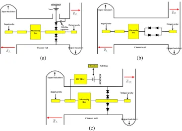
and thus the third harmonic can be obtained at output waveguide by using the matching circuit. The difference between two balanced triplers is mainly a on-chip capacitor needed in the circuit (as Figure 1(a)), which provides a DC bias to the varactor diodes. Commonly the capacitor is suitable for planar MMIC type frequency multipliers, hence this scheme is rarely adopted in domestic research. In consideration of feasibility of the circuit, a tripler without bias is proposed as shown in Figure 1(b). The disadvantages of this scheme are that the efficiency is relatively low, and heat accumulation happens in the Schottky junction when high input power is added due to the poor thermal conductivity of quartz glass (k = 1.4 W/m·K). To overcome these problems, a unbalanced scheme [13] with a pair of varactor chips in parallel is adopted as shown in Figure 1(c). Even though the even harmonics cannot be suppressed, hence the design process gets more difficult, unbalanced structure is suitable for designing high efficiency tripler with discrete Schottky diodes.
(a) (b)
(c)
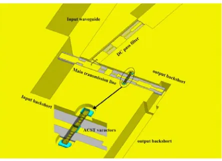
Figure 2. Bottom block of the 225 GHz unbalanced tripler, including a pair of quartz circuits used as DC pass filter and main transmission circuit respectively.
Figure 3. 3D model of diode cell in HFSS.
3. DESIGN TECHNIQUE
As depicted in Figure 2, the tripler is a split-block waveguide design, and a microstrip circuit based on 50µm thin quartz substrate is mounted in channel between the input and output waveguides. To provide the bias to diodes, another quartz circuit is brought in at the insensitive part of the main transmission line.
Field-circuit method is applied to the design process, so the tripler is divided into two parts: a liner network, which is analyzed using Ansys High Frequency Structure Simulator (HFSS) in consideration of the parasitic effects, and non-liner behavior of the varactor, solved by Agilent Advanced Design Simulator (ADS). Moreover, to reduce the complexity of the problem, the liner part is further broken up into three sections: diode cell, input and output circuits.
3.1. Three-Dimensional Modeling of the Diodes
In the design of a frequency multiplier, usually the first step is to determine the characteristics of the diodes such as the epitaxial layer doping and anode diameter. The parameters of discrete diodes, however, are confirmed when they leave the factory. Moreover, commercial diodes available for selection are few. For varactor, the first concern is that diode’s cutoff frequency should be much higher than the operating frequency, and then diodes which minimize the series resistance and maximize the capacitance variation are selected.
5VA diode chip provided by German company (Advanced Compound Semiconductor Technologies GmbH), which comprises a linear array of 3 varactors, is selected for the design of 225 GHz tripler. The dimension of the chip is 240µm×60µm (length, width respectively), and the semi-insulating GaAs substrate is 35µm thick. As the parasitic parameters caused by physical structure play an important role in affecting the performance of the tripler at terahertz wave range, the electromagnetic field around the diodes is calculated with HFSS. The active parts of the diodes are replaced with lumped ports on rectangles inside the epilayer [14–16] as shown in Figure 3. TheS-parameters of diode cell (regarded as an 8-ports network) are exported to the ADS for harmonic-balance simulation.
3.2. The Input and Output Circuits
Figure 5. Simplified circuit in the ADS. The tripler model is also regarded as a 9-port network.
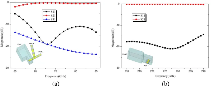
The S-parameters of the input circuit are clearly explained in Figure 4(a). From the simulated curve, it can be seen that the fundamental frequency is coupled to the main transmission line via an E-plane probe and passes through the filter to the diode cell (S21 parameter). Meanwhile, the DC
pass filter prevents the first harmonic from leaking into the bias circuit (S31 parameter). As shown in
Figure 4(b), another probe located in the output circuit couples the third harmonic to the standard output waveguide (S21 parameter). What needs to be explained is that the structural dimension (seen
as initial value) in HFSS will be optimized during the process of HB simulation in ADS.
3.3. Circuit Optimization
For optimization as a whole, the S parameter of each part is exported to ADS. Moreover, matching elements in the tripler are separated from the S-parameter matrix and replaced with discrete devices. Figure 5 shows the equivalent circuit of the tripler in ADS. Actually, the tripler model can also be regarded as a 9-port network, which includes the input waveguide port, output waveguide port, bias circuit port, and six lumped ports for Schottky diodes. The goal of above process is to obtain the desired conversion efficiency by adjusting the matching elements.
4. FABRICATION AND MEASUREMENT 4.1. Fabrication
(a) (b)
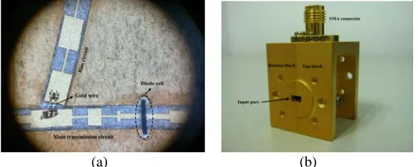
Figure 6. (a) Photo of the two quartz circuits mounted on the channels. (b) Photo of the assembled 225 GHz tripler block.
of bottom cavity with silver epoxy, and then heated for about an hour to solidify the adhesive. Second, a pair of diodes is mounted that one pad of each diode is glued on the transmission line of the quartz circuit, and the other pad is glued on the metal block. Another one hour is needed for heating. Then the bias quartz circuit is connected to the main transmission circuit by using gold wire bonding, and a SMA connector (type KFD76C) is introduced for DC feeding. Finally, the top and bottom blocks are jointed together with screws and pins. Figure 6(a) shows a photo of the quartz circuits under the microscope, and Figure 6(b) shows the photo of assembled tripler block.
4.2. Measurement
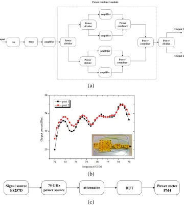
The power source used to drive the 225 GHz tripler mainly includes a sextupler, a power amplifier and a four-way power combiner module, and the composition block diagram is shown in Figure 7(a). The sextupler employs commercially available GaAs MMIC chip CHU 3377 fabricated by UMS company, and the power amplifier uses the MMIC chip APH633, fabricated by Hittite microwave corporation. At the output port of the power combiner module, aY-junction divider is applied to divide the power into two-way output. Figure 7(b) shows the measured results of the 75 GHz power source, which make clear that the output power of different ports have good consistency. Furthermore, the output power exceeds 26 dBm in a certain bandwidth range by removing theY-junction divider.
The block diagram of measurement setup is illustrated in Figure 7(c). An Agilent analog signal generator E8257D is followed by the power source, generating the signal over the 71–79 GHz band. An attenuator is added between the source and the DUT to control the input power (to DUT). The output power of the 225 GHz tripler is measured by PM4 power meter. Moreover, thanks to the unbalanced structure, the circuit has some dc current at high input levels. By introducing a resistor in the diode’s dc return path, this current can be used to bias the diode. Therefore, an external continuously variable potentiometer is connected to the SMA port.
Under the condition that the external biasing resistor’s value is 10 k ohms, the measured input and output powers of the tripler are plotted in Figure 8. It can be found that the output power is more than 7 dBm in 215∼228 GHz, and corresponding conversion efficiency is from 3% to 7.1%. The maximum output power is about 12.3 dBm at 224 GHz when driven with 23.8 dBm of input power at room temperature. Actually, the conversion efficiency relates to the input power and the value of biasing resistor. Therefore, another measurement is done to explain the relationship of the efficiency and above-mentioned variables. Corresponding results are shown in Figure 9. The efficiency changes along with the increasing of input power and reaches the peak value. Then the efficiency drops as the input power increases continuously (as Figure 9(a)). Moreover, the biasing resistor has an influence on the conversion efficiency. Figure 9(b) gives the measured results that the external resistor changes from 10 k to infinity at a fixed frequency (229 GHz), in which the highest conversion efficiency rises from 1.5% to 3.7%.
(a)
(b)
(c)
Figure 7. (a) The block diagram of 75 GHz (center frequency) source. (b) Measured results of the 75 GHz power source. (c) The block diagram of measurement setup.
(a) (b)
Figure 9. (a) Efficiency vs. input power (at fixed frequency point). (b) Efficiency vs. different bias resistor (taking a fixed frequency point 229 GHz for example).
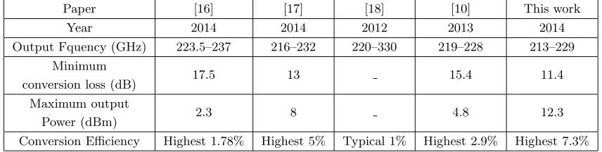
Table 1. Summary of the performance of domestic previous triplers and this work.
Paper [16] [17] [18] [10] This work
Year 2014 2014 2012 2013 2014
Output Fquency (GHz) 223.5–237 216–232 220–330 219–228 213–229 Minimum
conversion loss (dB) 17.5 13 15.4 11.4 Maximum output
Power (dBm) 2.3 8 4.8 12.3
Conversion Efficiency Highest 1.78% Highest 5% Typical 1% Highest 2.9% Highest 7.3%
improvement both in the design method and assembling process.
There are not many domestic reports on the design of tripler above 200 GHz. Table 1 demonstrates a simple comparison between the performance of other frequency triplers and this work.
5. CONCLUSION
An unbalanced 225 GHz tripler with discrete varactors has been designed and tested in this paper. The measured results show that this tripler has the ability to drive the mixer as a local oscillator source, which is important in the sub-millimeter receiver system. Our future work will be mainly focused on the model optimization [19, 20] and attempt to design wide band high-efficiency terahertz multiplier.
REFERENCES
1. Wang, H., A. maestrini, B. Thomas, et al., “Development of a two-pixel integrated heterodyne Schottky diode receiver at 183 GHz,”19th International Symposium on Space Terahertz Technology, 490–493, 2008.
2. Wang, H., “Design and modeling of monolithic circuits Schottky diode on a GaAs substrate at millimeter and submillimeter wavelengths heterodyne receivers for multi-pixel and on board satellites dedicated to planetary aeronomy,” Doctor Thesis, University of P&M Curie, Paris, 2009. 3. Hesler, J. L., “Planar Schottky diodes in submillimeter wavelength waveguide receivers,” Doctor
9. Schlecht, E., G. Chattopadhyay, A. Maestrini, et al., “200, 400, and 800 GHz Schottky diode substrateless multipliers: Design and results,” IEEE MTT-S International Microwave Symposium Digest, 1649–1652, 2001.
10. Meng, J., D.-H. Zhang, C.-H. Jiang, et al., “Research on the practical design method of 225 GHz tripler,” J. Infrated Millim. Waves, in Press.
11. Maestrini, A., B. Thomas, H. Wang, et al., “Schottky diode-based terahertz frequency multipliers and mixers,”Comptes Rendus Physique, Vol. 11, No. 7, 480–495, 2010.
12. Maestrini, A., J. S. Ward, J. J. Gill, et al., “A 540–640-GHz high-efficiency four-anode frequency tripler,”IEEE Transactions on Microwave Theory and Techniques, Vol. 53, No. 9, 2835–2843, 2005. 13. Porterfield, D. W., “High-efficiency terahertz frequency tripler,” IEEE MTT-S International
Microwave Symposium Digest, 337–340, Honolulu, Hawaii, 2007.
14. Marsh, S., B. Alderman, D. Matheson, and P. de Maagt, “Design of low-cost 183 GHz subharmonic mixers for commercial applications,”IET Circuits Devices Syst., Vol. 1, No. 1, 1–6, 2007.
15. Grajal, J., V. Krozer, E. Gonzalez, et al., “Modeling and design aspects of millimeter-wave and submillimeter-wave Schottky diode varactor frequency multipliers,” IEEE Transactions on Microwave Theory and Techniques, Vol. 48, No. 4, 700–712, 2000.
16. Zhang, Y., Q.-Q. Lu, and W. Liu, et al., “Design of a 220 GHz frequency tripler based om EM model of Schottky diodes,”J. Infrated Millim. WavesVol. 33, No. 4, 405–411, 2014.
17. Zhong, W., “Research on 220 GHz frequency multiplication technology based on Schottky barrier diodes,” School of Electronic Engineering, Chengdu, 2014.
18. Online: http://www.cas.cn/ky/kyjz/201210/t20121029 3668673.shtml.
19. Schlecht, E., G. Chattopadhyay, A. Maestrini, et al., “Harmonic balance optimization of terahertz Schottky diode multipliers using an advanced device model,” 13th Int. Symp. Space Terahertz Technology, 187–196, 2002.