Available online: https://edupediapublications.org/journals/index.php/IJR/ P a g e | 872
A New Five-Phase Coupled Inductor Inverter
With SVPWM Method for Common-Mode Voltage Reduction
1Patan Shali Basha, M.Tech, Email.Id: [email protected]
2 Dr.S.Suresh Reddy, Professor, Email.Id: [email protected]
NBKR Institute of Science and Technology, Vidyanagar,Andhra Pradesh, India
ABSTRACT-In this paper, two carrier-based pulse-width-modulation techniques are proposed to reduce the common-mode (CM) voltage generated by the five-phase inverter using space vector pulse width
modulation. This work presents multi-carrier
interleaved PWM strategies to control common mode voltage (CMV) in three phase coupled inductor inverter (CII). In this paper Space vector modulation (SVM) algorithm is used for the control of pulse width modulation (PWM).[1] It is used for the creation of alternating current (AC) waveforms. Carrier-based pulse-width-modulation techniques are popular due to their simplicity, and have been widely
researched for various three-phase inverter
configurations. The five-phase inverters have more flexibility in reducing the CM voltage than their three-phase counterparts because they have more phase legs hence finer control over the star-point voltage of the load. Two methods are proposed for the conventional two-level five-phase inverter to reduce the CM voltage; one utilizing adjacent modulating waveforms and the other utilizing non-adjacent
modulating waveforms. The coupled inductor
inverter (CII) uses coupled inductors to generate multi-level outputs. The proposed methods are further improved to ensure the volt-second integral over each switching period is zero. Moreover, the two proposed methods are designed to reduce switching events and prevent unexpected states occurring during the switching transitions. By using the simulation results we can analyse the performance and the switching strategy of both methods are verified using five-phase coupled inductor inverter.
I. INTRODUCTION
Multiphase inverters have been widely explored in recent decades, primarily as a method to drive multiphase machines [1] [2]. Compared with their three-phase counterparts, multiphase inverters have many advantages such as improved magnetomotive force (MMF) waveform, lower torque pulsation [3], higher torque density [4], and fault tolerance Common-mode (CM) voltage is one of the side effects in variable speed drive systems with PWM inverters. The high frequency CM voltage produces bearing currents via parasitic capacitance, which deteriorates the insulation, accelerates ageing, reduces the reliability and
ultimately leads to the failure of the machine [7][8]. In this paper Space Vector Modulation (SVM) Technique has become the important PWM technique for three phase Voltage Source Inverters for the control of AC Induction, Brushless DC, Switched Reluctance and Permanent Magnet Synchronous Motors. The study of space vector modulation technique reveals that space vector modulation technique utilizes DC bus voltage more efficiently and generates less harmonic distortion when compared with Sinusoidal PWM (SPWM) technique.
The side effects of the extra components are also apparent: more space is needed for the filters, applications of these filters are limited by the voltage and current ratings and failure probability of the system is increased due to there being more components. Reducing the CM voltage by updating the control strategies is preferred because this does not obviously increase the system cost and with the development of digital control ICs, the algorithms are not confined by limited resources of the previous digital controllers. The CM voltage was firstly researched in two-level inverters. However, as these inverters only have two output levels, the CM voltage can only be reduced with the control strategies rather than eliminated.
Several methods have been proposed to replace the zero vectors with different active vectors and these methods were reviewed in [21] from different aspects. Benefiting from the redundant vectors and extra output voltage levels, the multilevel inverters are able to eliminate the CM voltage. Many methods were proposed for different topologies aimed at eliminating or reducing the CM voltage proposed both space vector modulation (SVM) and sinusoidal pulse-width-modulation (SPWM) methods for the three-phase NPC system. A hybrid PWM method was proposed for open-end winding machine.
Available online: https://edupediapublications.org/journals/index.php/IJR/ P a g e | 873 inverters. It is a more sophisticated technique for
generating sine wave that provides a higher voltage to the motor with lower total harmonic distortion. The main aim of any modulation technique is to obtain variable output having a maximum fundamental component with minimum harmonics. Space Vector PWM (SVPWM) method is an advanced; computation intensive PWM method and possibly the best techniques for variable frequency drive applications.The main objectives of space vector pulse width modulation generated gate pulse are the following.
Wide linear modulation range
Less switching loss
Less total harmonic distortion in the spectrum of switching waveform
Easy implementation and less
computational calculations
A SVM method for a five-level inverter. [25] used predictive current control method for machine drive by only selecting switching vectors with minimum CM voltage to achieve a reduction of the CM voltage. The CM voltage in the multiphase machine drive system was also addressed. [29] The improved control methods are usually based on a star-connected load model, and then the CM voltage can be approximately expressed as the sum of the phase-to-midpoint (of the dc-link) voltages. Therefore, the essence of these methods, although they are proposed for different types of inverters, is similar, which is to choose the switching vectors so that the sum of the phase-to-midpoint voltages is minimum. The coupled inductor inverter (CII) is a competitive member in the family of multilevel inverters. In the three-phase system, the coupled inductors can utilize either three toroidal cores [30] or a more compact three-limb core [32][33].
Compared with the NPC topology [34], the advantages of CII topology are:
1. Fewer components required: to generate the same three-level output voltage, the CII only needs two switches and two diodes with the help of coupled inductor, which means the inverter semiconductor failure rate and the switching loss are reduced;
2. Dead-time is not required: Most voltage source inverters (VSI) have to use dead-time to prevent the shortcircuit of the dc-link, and the downside is obvious—distortion in the load current. However, due to the coupled inductor, the state in which both switches are ON is used to generate the middle level of the output voltage.
3. Low harmonic distortion on the load current: besides the absence of the dead-time, the CII improves the quality of the load current with
the coupled inductor which functions as a filter. Thus, extra filters between the inverter and the machine can be avoided, which reduces the system cost [35].
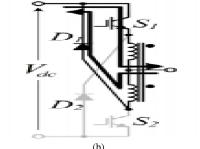
Fig. 1. Topology of the five-phase CII. In this paper, the reduction of CM voltage is studied in the five-phase CII system with five toroidal cores. Two general carrier-based pulse-width-modulation (CBPWM) techniques are proposed to reduce the CM voltage for the multilevel inverters. Then these two methods are improved to achieve volt-second balance on the magnetic cores, hence they can be applied to the five-phase CII system. This improvement also assures fewest switching events when the balance is achieved.
This paper is organized as follows: firstly, the operating principle of the CII is explained and a CBPWM method is proposed for the normal operation of the single phase leg of the CII; Secondly, two CBPWMs with the reduction of the CM voltage for multiphase multilevel inverters are proposed and improvements of these two CBPWMs are introduced so that they are applicable to the five-phase CII system and the fewest switching events happen in the methods. Finally, the methods are verified by simulations.
FIVE-PHASE COUPLED INDUCTOR INVERTER
Coupled Inductor Inverter
Available online: https://edupediapublications.org/journals/index.php/IJR/ P a g e | 874 capable of generating three levels: -Vdc/2, 0Vdc,
and +Vdc/2.
In three-phase inverters, the cores of the coupled inductors can be either toroidal cores or three-limb cores [30][31]. For the five-phase case, a five-limb core is not an off-the-shelf item, and a customized core will increase the cost of the system. Therefore, in this paper, the coupled inductors are made of five individual toroidal cores. From Fig. 2(a), the following holds:
𝑖0= 𝑖𝑢𝑝− 𝑖𝑑𝑡 (1) whereio is the load current, iup is the current in the upper arm of the coupled inductor and idn the current in the lower arm of the coupled inductor. The currents in the two arms share certain
(a)
Fig. 2. Four states of one leg of the coupled-inductor inverter: (a) topology of single leg CII; components, including the dc-offset and high frequency component. These components are represented by icm. The four normal working states are shown in Fig. 2(b)-(e), and the arrows represent the current directions, showing that the CII supports bidirectional current flow.
(b)
Fig. 2. Four states of one leg of the coupled-inductor inverter: (b) State1: outputs +Vdc/2 level;
When the phase leg is in State1, Fig. 2(b), the current flows into the load via S1 and out from the load via D1; when the topology is in State2, Fig. 2(c), the current flows into the load via D2 and out from the load via S2;
(c)
Fig. 2. Four states of one leg of the coupled-inductor inverter: (c) State2: outputs –Vdc/2 level;
when the topology outputs 0Vdc, S1 and S2 can be both ON, Fig. 2(d) or OFF, Fig. 2(e).
(d)
Fig.2. Four states of one leg of the coupled-inductor inverter: (d) State3: outputs 0Vdc level,
the coupled inductor is energized;
In State3, Fig. 2(d), the coupled inductor is energized due to the directly imposed dc-link voltage so that the current in the coupled inductor rises. Vice versa, in Fig. 2(e), the coupled inductor is de-energized due to the reversely imposed dc-link and the current flows through two diodes (D1 and D2), and decreases.
(e)
Fig.2. Four states of one leg of the coupled-inductor inverter :(e) State4: outputs 0Vdc level,
Available online: https://edupediapublications.org/journals/index.php/IJR/ P a g e | 875 positive; when the iup is smaller than idn, the load
current is negative. It is also noticeable that in State3 and State4, the current in the coupled inductor rises/falls much faster than in State1 and State2. As a result, the rate of change of the currents in the coupled inductor in State1 and State2 is much smaller than that in State3 and State4, due to the low imposed voltage. As the CII is operated with PWM methods, the currents iup, and idn also include high-frequency components, and here they are represented as ihf,up for those in the upper arm, and ihf,dn for those in the lower arm. Finally, it is seen that, in State3, Fig. 2(d) and State4, Fig. 2(e), a zero-sequence component flows through the coupled inductor which produces a dc-offset current. It is represented by idc. Therefore, the currents in the two arms can be described as:
𝑖𝑢𝑝 = 𝑖𝑓+ 𝑖ℎ𝑓,𝑢𝑝+ 𝑖𝑑𝑐 (2) 𝑖𝑑𝑛= −𝑖𝑓+ 𝑖ℎ𝑓,𝑑𝑛+ 𝑖𝑑𝑐 (3)
whereif is the fundamental-frequency component [35]. The if in two arms are chosen with the displacement of 180˚, for the sake of convenient control. When iup and idn are substituted in (2) into (1), the load current is:
𝑖𝑜= 2𝑖𝑓+ 𝑖ℎ𝑓,𝑢𝑝− 𝑖ℎ𝑓,𝑑𝑛 (4) Hence, the load current only contains the fundamental frequency and high-frequency components.
Carrier Based PWM for the Coupled Inductor Inverter
In the conventional PWM for the NPC, the modulating waveform is compared with the triangular carriers: if the modulating waveform is equal or higher than the carrier, a switching-on signal is generated; if the former is smaller than the latter, a switching-off signal is generated. In the CBPWM method for CII proposed in [30]: two opposite carriers, which represent the upper switch (S1) and the lower switch (S2), are compared with one sinusoidal modulating waveform; the control signal for S1 is obtained according the above rule, whereas the control signal of S2 is obtained after the inversion of the signal obtained from the comparison of S2’s carrier and the modulating waveform.
CBPWM METHOD FOR SINGLE LEG CII SYSTEM
In this section, a CBPWM method for the single leg CII is proposed. This technique directly follows the working principle of the coupled inductor and can naturally balance the volt-second, whereas the CM voltage is not reduced.
Proposed CBPWM for single-leg CII
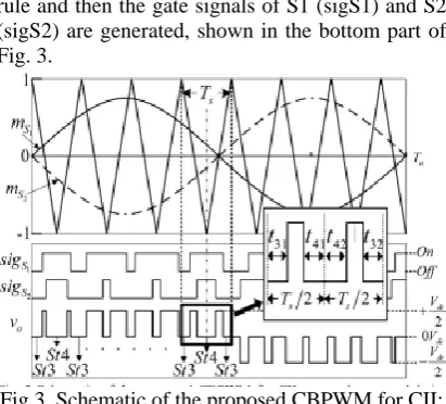
In this paper, according to the aforementioned analysis, a CBPWM technique is proposed which achieves the same effect as the
previous carrier-based method for CII but is simpler to realize. The schematic of the proposed CBPWM is shown in Fig. 3, top part: two modulating waveforms (mS1 and mS2), which have a displacement of 180˚, represent two switches (S1 and S2); theyare compared against a triangular carrier abiding by the conventional PWM rule and then the gate signals of S1 (sigS1) and S2 (sigS2) are generated, shown in the bottom part of Fig. 3.
Fig.3. Schematic of the proposed CBPWM for CII: mS1 and mS2: modulating waveforms for the upper switch S1 and the lower switch S2; sigS1 and sigS2 are the resulting gate signals generated by the
comparison between mS1 and the carrier, and between mS2 and the carrier; vo is the output
voltage of one leg.
Finally, the output voltage of one leg, vo, is obtained according to the states of two switches. The principle of this technique directly describes the operating principle of coupled inductor: by making the switches work out of phase, the two arms of the coupled inductors are imposed with the voltage pulses having opposite fundamental sinusoidal elements so that the currents in these two arms are opposite. Consequently, the load current will follow (3).
Natural Flux Balance
Available online: https://edupediapublications.org/journals/index.php/IJR/ P a g e | 876 are the first and the second duration of State4.
Because the modulating waveforms mS1 and mS2 are opposite, t31 equals to t41 and t32 equals to t42. Thus the durations of State3 and State4 are the same, which means the requirement of the volt-second balance is satisfied.
PROPOSED CBPWM METHOD WITH REDUCTION OF COMMON-MODE
VOLTAGE IN FIVE-PHASE CII In this section, CBPWM methods to cancel the CM voltage for five-phase inverters are proposed. Then the proposed methods are improved so that they can be applied to the five-phase CII system for the sake of volt-second balance. Theimproved methods also reduce switching events. Finally, the procedures of these methods are illustrated.
Common-mode Voltage
One of the side effects from the basic PWM process is an increased common-mode (CM) voltage. As shown in Fig. 1, the CM voltage, vnN, is defined here as the potential of node “n” with respect to the node “N”. The frequency of the CM voltage can be equal to or higher than the switching frequency. When the inverters are connected to machines, this high-frequency voltage will produce bearing current via parasitic capacitance, leading to premature ageing of the insulation or bearing. Moreover, the CM voltage has other negative impacts such as causing vibration to the machine and producing EMI which potentially disrupts other electrical devices. In the five-phase inverter with balanced load in star-connection, the CM voltage is defined as follows:
𝑣𝑛𝑁=15(𝑣𝐴𝑁+ 𝑣𝐵𝑁+ 𝑣𝐶𝑁+ 𝑣𝐸𝑁) (5) Elimination of CM Voltage in Five-Phase Inverters
Similarly, as discussed in [35] for the three-phase case, vnN = 0 is the requirement to eliminate the CM voltage in five-phase inverters. However, there are two ways to obtain this, shown in (5) and (6):
𝑣𝑛𝑁=15[(𝑣𝐴𝑁− 𝑣𝐵𝑁) + (𝑣𝐵𝑁− 𝑣𝐶𝑁) + (𝑣𝐶𝑁− 𝑣𝐷𝑁) + (𝑣𝐷𝑁− 𝑣𝐸𝑁) + (𝑣𝐸𝑁− 𝑣𝐴𝑁)]=0
(6)
which uses the two adjacent modulating waveforms and is called Method1;
𝑣𝑛𝑁=1
5[(𝑣𝐴𝑁− 𝑣𝐶𝑁) + (𝑣𝐵𝑁− 𝑣𝐷𝑁) + (𝑣𝐶𝑁− 𝑣𝐸𝑁) + (𝑣𝐷𝑁− 𝑣𝐴𝑁) + (𝑣𝐸𝑁− 𝑣𝐵𝑁)] = 0
(7)
which uses the non-adjacent modulating waveforms and is called Method2. Although the two methods are using two different waveforms, their weighted total harmonic distortion (WTHD)
performances are similar, which will be shown in Section VII.
Fig.4. Schematic of CBPWM with CM voltage elimination for five-phase inverters: mA and mB
are the modulating waveforms of Phase A and Phase B; pA and pB are the results of the comparisons between mA and the carrier, and between mB and the carrier; vAN is the expected
output voltage of Phase A.
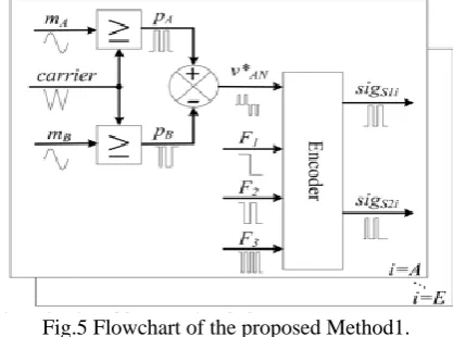
Fig. 4 shows the waveforms of Method1, the outputwaveform of Phase A and uses the same legends as Fig. 3. Fig. 5 displays the flowchart of realizing Method1.
Step1: PWM signals (pA and pB) are obtained by comparing the modulating waveforms of Phase A and Phase B (mA and mB) respectively with the carrier;
Step2: signal v*AN is obtained by subtracting pB from pA; this signal will also be the pattern of the output voltage of Phase A (vAN);
Step3: An encoder is designed to translate v*AN into control signals of two switches in Phase A. The signals F1, F2 and F3, Fig. 5, are additional signals for the CII system. After these three steps, the gate driver signals of the two switches in Phase A are obtained.
Available online: https://edupediapublications.org/journals/index.php/IJR/ P a g e | 877 CII system, an extra step is required to identify the
position of two 0Vdc states so that the volt-second is balanced.CM Voltage Reduction for Five-phase CII with CBPWM methods
If the methods are implemented directly on the CII with State3 and State4 appearing in turns, large in-phase currents are generated in the coupled inductors (greater than ten times the current rating in the simulation). As shown in Fig. 4, because the phase displacement of mA and mB is not 180˚, the durations of State3 and State4 are not equal: in the inset, t31 is much smaller than t41, and as is the case for t32 and t42.
The solution is demonstrated in Fig. 6 which shows three switching periods. Because the switching period is much shorter than the output period, mA (solid) and mB (dotted) are represented by straight lines; SigS1 and SigS2 represent the final gate signals of two switches in one leg.
TABLE I TRUTH TABLE OF THE FINITE STATE MACHINE
Firstly, in order to reduce switching losses (because the transition between State3 and State4 requires two switches to change state at the same time), the end of one switching period and the beginning of its next switching period should have identical states.
Fig. 6. Schematic of CBPWM with CM voltage elimination for CII: mA and mB are the modulating waveforms of Phase A and Phase B; pA and pB are
the results of the comparisons between mA and the carrier, and between mB and the carrier; t31 and t32 are the durations of State3; t41 and t42 are the
durations of State4; SigS1 and SigS2 are the control signals for S1 and S2 in one phase leg.
For instance, in Fig. 6, the second switching period is joined to the first period by State4 and the third is joined to the second via State3. Secondly, in the middle of the switching period, the direct transition from State3 to State4 or from State4 to State3 is inevitable for the sake of volt-second balance. If State3 appears before State4, the two switches in the same leg have different turn-off times when they are conducting different currents:
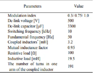
TABLE II PARAMETERS IN SIMULATION
The truth table of the encoder for the CII system is given in Table I. F1, F2 and F3 are only considered when v*AN is 0. State3 and State4 respectively occupy four of eight states produced by the combination of the three additional signals. SPACE VECTOR CONCEPT
The space vector concept, which is derived from the rotating field of induction motor, is used for modulating the inverter output voltage. In this modulation technique the three phase quantities can be transformed to their equivalent two-phase quantity either in synchronously rotating frame (or) stationary frame. From these two-phase components, the reference vector magnitude can be found and used for modulating the inverter output. The process of obtaining the rotating space vector is explained in the following section, considering the stationary reference frame. Considering the stationary reference frame let the three-phase sinusoidal voltage component be,
Va = VmSinωt(8) Vb = VmSin(ωt-2π/3) (9) Vc = VmSin(ωt-4π/3) (10)
Available online: https://edupediapublications.org/journals/index.php/IJR/ P a g e | 878 flux can be represented as single rotating voltage
vector. The magnitude and angle of the rotating vector can be found by means of Clark’s Transformation as explained below in the stationary reference frame. To implement the space vector PWM, the voltageequations in the abc reference frame can be transformed intothe stationary dq reference frame that consists of the horizontal (d) and vertical (q) axes as depicted in Figure-2.
Fig.7 The relationship of abc reference frame and stationary dq reference frame.
As described in Figure-7. This transformation is equivalent to an orthogonal projection of [a b c] t onto the two-dimensional perpendicular to the vector [1 1 1] t (the equivalent d-q plane) in a three-dimensional coordinate system. As a result, six non-zero vectors and two zero vectors are possible. Six non-zero vectors (V1-V6) shape the axes of a hexagonal as depicted in Figure-8, and supplies power to the load.
Fig.8. Basic switching, vectors and sectors
The angle between any adjacent two non-zero vectors is 60 degrees. Meanwhile, two non-zero vectors (V0 and V7) and are at the origin and apply zero voltage to the load. The eight vectors are called the basic space vectors and are denoted by (V0, V1, V2, V3, V4, V5, V6, V7). The same transformation can be applied to the desired output voltage to get the desired reference voltage vector,Vref in the d-q plane. The objective of SVPWM technique is to approximate the reference voltage vector Vref using theeight switching patterns. One simple method of approximation is to generate the average output of the inverter in a small period T to be the same as that of Vref in the same period.
Table:III Switching patterns and output vectors
SIMULATION RESULTS
In this section, the methods are simulated in MATLAB, and simulated results of both Method1 and Method2 are shown. The simulations are performed with three modulation indices: 0.3, 0.75 and 1.0 which represent the linear modulation range of the CII. The modulation index is defined as:
𝑀 = 𝑉𝑟𝑒𝑑
𝑣𝑑𝑐√2 (11)
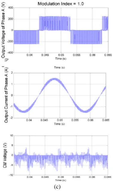
whereVref is the reference voltage and Vdc is the dc-link voltage. Simulations and experiments share the parameters in Table II. Fig. 7 shows the simulated results of Method1 at different modulation indices. It is clear that the CM voltages at all three modulation indices are almost zero (less than 10V, which is 2% of the dc-link voltage). Fig. 8 shows the simulated results of Method2.
Available online: https://edupediapublications.org/journals/index.php/IJR/ P a g e | 879 (a)
(b)
(c)
Fig. 9. Simulated results of Method1 (time scale 5ms/div): (a) modulation index = 0.3; (b) modulation index = 0.75; (c) modulation index =
1.0; the first row: the load voltage of Phase A, 200V/div; the second row: the load current of Phase A, 1A/div, the third row, the CM voltage,
5V/div.
Available online: https://edupediapublications.org/journals/index.php/IJR/ P a g e | 880 (a)
(b)
(c)
Fig.10. Simulated results of Method2 (time scale 5ms/div): (a) modulation index = 0.3; (b) modulation index = 0.75; (c) modulation index =
1.0; the first row: the load voltage of Phase A, 200V/div; the second row: the load current of Phase A, 1A/div, the third row, the CM voltage,
5V/div.
It is seen that the CM voltage is successfully reduced to almost zero, in spite of some residual CM voltages which are less than 5V.
CONCLUSION
A carrier-based PWM technique for the five-phase coupled inductor inverter (CII) is proposed in this paper. This method uses two opposite sinusoidal waveforms which are compared with a carrier to control the switches in one phase leg. This technique is a more intuitive method of PWM compared with existing techniques and helps develop a better understanding ofthe operating principle of the coupled inductor in the inverter. Space vector PWM is an advanced technique used for variable frequency drive applications. It utilizes dc bus voltage more effectively and generates less THD in the Three Phase Voltage Source Inverter Two alternative carrier-based PWM methods are then proposed for the five-phase inverter so as to reduce the common-mode (CM) voltage. These two methods are further improved to balance the volt-second in the coupled inductors; hence, in-phase currents in the coupled inductors are avoided. The two methods are verified in simulation and they successfully reduce the CM voltage to almost zero.
REFERENCES
Available online: https://edupediapublications.org/journals/index.php/IJR/ P a g e | 881 Elect. Power Appl., vol. 1, no. 4, pp. 489-516, Jul.
2007.
[2] E. Levi, "Multiphase electric machines for variable-speed applications," IEEE Trans. Ind. Electron., vol. 55, no. 5, pp. 1893-1909, May 2008.
[3] S. Williamson and S. Smith, "Pulsating torque and losses in multiphase induction machines," IEEE Trans. Ind. Appl., vol. 39, no. 4, pp. 986-993, July/Aug. 2003.
[4] R. O. C. Lyra and T. A. Lipo, "Torque density improvement in a six-phase induction motor with third harmonic current injection," IEEE Trans. Ind. Appl., vol. 38, no. 5, pp. 1351-1360, Sept./Oct. 2002.
[5] N. Nguyen, F. Meinguet, E. Semail, and X. Kestelyn, "Fault-tolerant operation of an open-enopen-end winding five-phase PMSM drive with short-circuit inverter fault," IEEE Trans. Ind. Electron., early access.
[6] H. Guzman, F. Barrero, and M. J. Duran, "IGBT-gating failure effect on a fault-tolerant predictive current-controlled five-phase induction motor drive," IEEE Trans. Ind. Electron., vol. 62, no. 1, pp. 15-20, Jan. 2015.
[7] C. Shaotang, T. A. Lipo, and D. Fitzgerald, "Modeling of motor bearing currents in PWM inverter drives," IEEE Trans. Ind. Appl., vol. 32, no. 6, pp. 1365-1370, Nov. 1996. [8] S. Chen, T. A. Lipo, and D. Fitzgerald, "Source of induction motor bearing currents caused by PWM inverters," IEEE Trans. Energy Convers., vol. 11, no. 1, pp. 25-32, Aug. 1996.
[9] A. Willwerth and M. Roman, "Electrical bearing damage-- a lurking problem in inverter-driven traction motors," in Proc. IEEE ITEC, 2013, pp. 1-4.
[10] M. C. Di Piazza, A. Ragusa, and G. Vitale, "Effects of common-mode active filtering in induction motor drives for electric vehicles," IEEE Trans. Veh. Technol., vol. 59, no. 6, pp. 2664-2673, Jul. 2010.
[11] D. Cochrane, D. Y. Chen, and D. Boroyevic, "Passive cancellation of common-mode noise in power electronic circuits," IEEE Trans. Power Electron., vol. 18, no. 3, pp. 756-763, May 2003.\
[12] V. Dzhankhotov, J. Pyrhonen, P. Silventoinen, M. Kuisma, and T. A. Minav, "A new passive hybrid air-core foil filter for modern power drives," IEEE Trans. Ind. Electron., vol. 58, no. 5, pp. 1757-1762, May 2011.
[13] M. H. Hedayati, A. B. Acharya, and V. John, "Common-mode filter design for PWM rectifier-based motor drives," IEEE Trans. Power
Electron., vol. 28, no. 11, pp. 5364-5371, Nov. 2013.
[14] M. L. Heldwein, L. Dalessandro, and J. W. Kolar, "The three-phase common-mode inductor: modeling and design issues," IEEE Trans. Ind. Electron., vol. 58, no. 8, pp. 3264-3274, Aug. 2011.