Simulation of a Multi-Level Inverter with
DC-Link Switches for Power factor Control using
Matlab/Simulink
J.Lakshmi Prasad1, B.Shilpa2Assistant Professor, Dept. of EEE, Anantha Lakshmi Institute of Technology and Sciences, Ananthapuramu,
A.P, India1
PG Student, Dept. of EEE, Anantha Lakshmi Institute of Technology and Sciences, Ananthapuramu, A.P, India 2
ABSTRACT: This paper is based on Bridge structure which proposes a multi-level inverter topology. Here H-Bridge structure with 4 switches connected to DC link. A new PWM method based on POD which required only one carrier signal. Switching sequence to balance the capacitor voltages required Minimum no. of components count to increase the no. Of voltage levels required. The proposed topology simulation is used to verify operating principle of proposed inverter.
KEYWORDS: PWM, DC-link switches, Multi-level inverters, powerfactor.
I.INTRODUCTION
Multilevel inverters is attracting in favor of academia as well as industry in the recent decade for high-power and medium-voltage energy control. In addition, they can synthesize switched waveforms with lower levels of harmonic distortion than an equivalently rated two-level converter [7]. The multilevel concept is used to decrease the harmonic distortion in the output waveform without decreasing the inverter power output. This paper presents the most important topologies like diode-clamped inverter (neutral- point clamped), capacitor-clamped (flying capacitor), and cascaded multilevel [6] with separate dc sources. This paper also presents the most relevant modulation methods developed for converters: multilevel sinusoidal pulse width modulation, multilevel selective harmonic elimination, and space-vector [11] modulation. Authors strongly believe that this survey article will be very much useful to the researchers for finding out the relevant references in the field of topologies and modulation [2] strategies of multilevel inverter. Increasing the number of voltage levels [6] in the inverter without requiring higher ratings on individual devices can increase the power ratings. The unique structure of multilevel voltage source inverters allows them to reach high voltages with low harmonics without the use of transformers [5] or series connected synchronized switching devices.The topological structure of multilevel inverter must
i) have less switching devices as far as possible
ii) be capable of withstanding very high input voltage for high power applications
iii) have lower switching frequency[3] for each switching device
The features of multilevel inverters are,
i) The output voltage and power increase with number of levels
The advantages are,
i) They are suitable for high voltage and high current applications
ii) They have higher efficiency because the devices can be switched at a low frequency
iii) Power factor [1] is close to unity
iv) No EMI problem exists
II. CONNECTION OF MULTI-LEVEL INVERTER:
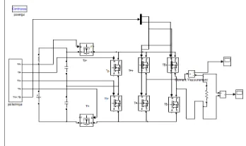
As shown in Fig1. , the proposed MLI is composed of two dc-link capacitors (C1, C2) and four switching devices (TA +,TA-, TB+, TB-) comprising a H-bridge, and four active switches(TP+, TP-, TN+, TN-) located between dc-link and H-bridge. The voltage across the switching devices in the dc-link [2] (TP+, TP-, TN+, TN-) is VDC/2 and operated at a switching frequency. Whereas, voltage across the switching devices in the H-bridge (TA+, TA-, TB+, TB-) is VDC and the switches (TA+, TA-, TB+, TB-) are switched at a frequency of the fundamental component of the output voltage (e.g. 50 or 60 Hz). Thus, the dc-link switches (TP+, TP-, TN+, TN-) and the H bridge [13] switches (TA+, TA-, TB+, and TB-) can be strategically selected based on the rated power of the inverter system in order to reduce system cost and increase efficiency.
Fig 1 single phase multi-level inverter
III. OPERATING MODES AND PROPOSED PWM STRATEGY:
The output voltage of the proposed MLI shown in Fig. has five levels (VDC, VDC/2, 0, -VDC/2, -VDC) according to the switching states of the inverter. There are four operation modes depending on the instantaneous value of the reference voltage, Vref and the maximum value of the carrier signal [4], VC. Table shows the possible inverter output voltage level according to the operating mode. In case of the N-level NPC type multi-level inverter, N-1 triangular carrier signals with the same frequency and amplitude are used so that they fully occupy contiguous bands over the range +VDC to -VDC. A single sinusoidal reference is compared with each carrier signal to determine the output voltage for the inverter [10]. Three dispositions of the carrier signal are considered to generate the PWM signal. 1) Phase disposition (PD); where all carriers are in phase.
2) Alternative phase opposition disposition (APOD); where each carrier is phase shifted by 180 degree from its adjacent carrier.
3) Phase opposition disposition (POD); where the carriers above zero voltage are 180 degree out of phase with those below zero voltage.
The generation of the PWM signal for dc-link switches (TP+, TN-) can be explained as follows.
∙ Mode 1: a signal subtracted from the reference signal by Vc is compared with the carrier signal. If vref -Vc> vcarrier, then all switches TP+ and TN- are turned on. If vref -Vc< vcarrier, then the switch TP+ or TN- is turned off alternately.
∙ Mode 2: the reference signal is directly compared with a carrier signal. If vref > vcarrier, then the switch TP+ or TN- is turned on alternately. If vref < vcarrier, then all switches TP+ and TN- are turned off.
∙ Mode 3: -vref is directly compared with a carrier signal.If -vref > vcarrier, then the switch TP+ or TN- is turned onalternately. If -vref < vcarrier, then all switches TP+ and TN- are
turned off.
∙ Mode 4: a signal subtracted from -vref by Vc is compared with the carrier signal. If If -vref -Vc> vcarrier, then all switches TP+ and TN- are turned on. If -vref -Vc< vcarrier, then the switch TP+ or TN- is turned off alternately.Only one carrier signal is used to generate eight PWM signals in the proposed PWM method. Thus it is quite simple.
IV. VOLTAGE BALANCING OF DC-LINK CAPACITOR
One of the important issues about multi-level inverter is the voltage balance of the dc-link capacitor. The voltage of capacitor C1 and C2 should be equally balanced to VDC/2. However the midpoint voltage fluctuates when C1 and C2 Charge and discharge continuously [5]. If the capacitor voltage is unbalanced [11], the output voltage becomes unsymmetrical and it results in a high harmonic content in the load current. To solve this problem, the switching state should be selected appropriately. If only one switch in a dc link is turned on, the output voltage becomes VDC/2. In order to balance the voltage of dc-link capacitor, dc-link switches (TP+, TN-) are alternately turned on at mode 2, and alternately turned off at mode 1. And switches (TP-, TN+) are operated complementally to switches (TP+, TN-). The switching sequence of mode 3 and mode 4 are similar that of mode 1 and mode 2.
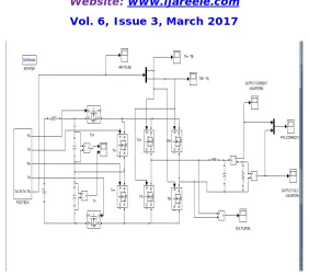
Fig 3 : Power Factor Correction
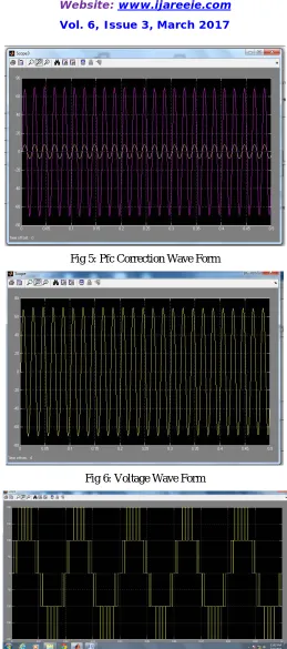
The proposed 9-level inverter is tested to verify the operating principle of the proposed MLI. The LC filter is inserted between the output of the inverter and the load. Electrical specifications of the proposed inverter are summarized Fig. 6 and 9 show simulation waveforms of the proposed inverter in 9-level. Fig. 4 shows the waveforms of the inverter output voltage, load voltage and the load current when the power factor becomes unity. Fig. 8 shows the waveforms of the inverter output voltage, load voltage and the load current during the lagging power factor.
VI. RESULTS AND DISCUSSION
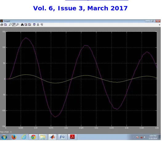
Fig 5: Pfc Correction Wave Form
FIG 8:Output Voltage and Current
VII. CONCLUSION
This paper proposed a new multi-level inverter topology based on a H-bridge inverter with four switches connected to the dc-link.
1. Number of devices of the proposed multi-level inverter is fewer than that of the conventional multi-level inverters. It is reliable and cost competitive than the conventional two-level and multilevel inverters.
2. The 4 switches in the H-bridge are switched at a low frequency (e.g. 60 Hz). Switching losses are very low. 3. For 4 switching devices Only one carrier signal is required to generate the PWM signals.
4. This concept is extended to 9-level or higher level with minimized active device component count.
REFERENCES
[1] D.A.B. Zambra, C. Rech, J.R. Pinheiro, "Comparison of Neutral-Point- Clamped, Symmetrical, and Hybrid Asymmetrical Multilevel Inverters", IEEE Trans. Ind. Electron., Vol. 57, no. 7, pp2297-2306, July 2010.
[2] M. Calais, "Analysis of multicarrier PWM methods for a single-phase five level inverter", PESC. 2001 IEEE, Vol. 3, pp. 1351-1356, 2001. [3] G. Grandi, C. Rossi, D. Ostojic, D. Casadei, "A New Multilevel Conversion Structure for Grid-Connected PV Applications", IEEE Trans. Ind. Electron., vol. 56, no. 11, pp. 4416-4426, Nov. 2009.
[4] N. A. Rahim, S. Mekhilef, “Implementation of Three- Phase grid Connected Inverter for Photovoltaic Solar Power Generation System” Proceedings IEEE. PowerCon 2002. Vol. 1, pp. 570-573., Oct 2002
[5] A. Nabae, I. Takahashi and H. Akagi, “A New Neutral-Point-Clamped PWM Inverter” IEEE Trans. Ind. Appl., vol. 1A-17, no. 5, pp. 518-523, Sep. 1981.
[6] Y. Liang, C.O. Nwankpa, "A power-line conditioner based on flyingcapacitor multilevel voltage source converter with phase-shift SPWM" IEEE Trans. Industrial Electronics, Vol. 36, pp. 965-971, 2000.
[7] E. Villanueva, P. Correa, M. Pacas, “Control of a Single-Phase Cascaded H-Bridge Multilevel Inverter for Grid-Connected Photovoltaic Systems”, IEEE Trans. Industrial Electronics, Vol. 56, pp. 4399-4406, 2009.
[8] O. Lopez, R. Teodorescu, J. Doval-Gandoy, "Multilevel transformerless topologies for single-phase grid-connected converters" IEEE. IECON 2006, pp. 5191-5196, 2006.
[9] Tae-Jin Kim, Dae-Wook Kang, Yo-Han Lee and Dong-Seok Hyun, “The analysis of conduction and switching losses in multi-level inverter system”, PESC. 2001 IEEE Vol. 3, pp 1363-1368, 2001.
[10] B.P. McGrath, “Multicarrier PWM strategies for multilevel inverters”, IEEE Trans. Ind. Electron., Vol. 49, no. 4, pp. 858-867, 2002.