ePrints Soton
Copyright © and Moral Rights for this thesis are retained by the author and/or other
copyright owners. A copy can be downloaded for personal non-commercial
research or study, without prior permission or charge. This thesis cannot be
reproduced or quoted extensively from without first obtaining permission in writing
from the copyright holder/s. The content must not be changed in any way or sold
commercially in any format or medium without the formal permission of the
copyright holders.
When referring to this work, full bibliographic details including the author, title,
awarding institution and date of the thesis must be given e.g.
FACULTY OF ENGINEERING, SCIENCE &
MATHEMATICS
OPTOELECTRONICS RESEARCH CENTRE
TAPERED WAVEGUIDE LASERS
bySimon James Hettrick
Thesis submitted for the degree of Doctor of Philosophy
ABSTRACT
FACULTY OF ENGINEERING, SCIENCE AND MATHEMATICS OPTOELECTRONICS RESEARCH CENTRE
Doctor of Philosophy
TAPERED WAVEGUIDE LASERS. By Simon James Hettrick
The work reported in this thesis concerns the design and fabrication of tapered waveguide lasers to allow efficient, high-power diode-pumping and produce diffraction-limited, near-symmetrical output, whilst maintaining a monolithic de-sign compatible with integrated optical circuits.
The design rules required for efficient operation of a tapered waveguide are derived, and applied to the fabrication of tapered waveguides by thermal ion ex-change (TIE) in Nd-doped borosilicate glass. Ti:sapphire pumped laser operation of these waveguides indicates efficient (40%) and low-loss (0.2dBcm−1)
opera-tion, comparable to that of a channel waveguide fabricated within the same sub-strate. Parabolic and linear taper shapes are compared, and the linear shape is found to provide superior operation at wide taper expansions (up to250µm, over a length of≈22mm), and hence is more suited to end-pumping with multi-watt broad-stripe-diodes. Broad-stripe-diode end-pumping is also investigated, and the laser performance is characterised, indicating a need to control the refractive index profile to maximise the overlap of the multimode-pump and single-mode laser. Field-assisted ion exchange is therefore investigated to improve the over-lap of the diode-pump and laser modes in a tapered waveguide. Waveguides produced by this technique are shown to exhibit the desired step-like index pro-file, but require further optimisation to improve the laser performance.
Low-loss (0.1dBcm−1) operation of a tapered waveguide laser is reported in a hybrid Nd-doped/undoped borosilicate glass. The hybrid glass is proposed as a useful substrate for reducing the quasi-3-level reabsorption loss of Yb3+-doped
lasers. As an initial step towards this goal, channel waveguides are fabricated in standard Yb3+-doped phosphate glass, which exhibit efficient (50–75%) and
moderate-loss (0.6dBcm−1) laser operation.
The design requirements for a power scalable diode-side-pumped tapered waveguide laser are also investigated, and YVO4 is proposed as a suitable
Over the past four years I’ve been really looking forward to writing the ac-knowledgements, however, thanking everyone that has helped me through this time - in one page - is going to be difficult. Here goes:
Firstly, I’d like to thank my supervisor Dave Shepherd for his constant help, optimistic attitude and the look of panic he does when you say some-thing stupid before the vi va. Cheers Dave!
I’d also like to thank Jacob Mackenzie (Matchcad Man) and Cheng Li for the diode-pumping, Dave Sager and Neil Sessions the cleanroom Guru’s and Angelique Favre for the glass bonding.
Outside of work (the best place to be in my opinion) I’ve found a num-ber of people without whom life would have been very dull. The most notable culprits are Taj Bhutta for providing advice galore, being useless at Goldeneye and his somewhat savage critique of my writing. Denis Guil-hot - next for the chop - who came round every Thursday to see if I was still alive, then cooked my lunch and listened to me rant about Physics for an hour, and Barry Dunne for being delightfully non-ORC and thrashing me repeatedly at chess. I’d also like to thank the transient population of office 2071 for the larking about over the years, don’t let the portacabin break the Babylon ethic. And make them give you shelves.
My Mum and Dad who not only had to put up with laser-based con-versations bordering on the torturous, but paid me to do it! Thanks for the support, and I hope you’re not upset that the thesis has nothing to do with floppy disks.
Abstract i
Quote ii
Acknowledgements iii
Contents iv
1 Introduction 1
1.1 Diode-pumped Solid-State Lasers . . . 1
1.2 The Waveguide Geometry . . . 2
1.2.1 Waveguide Lasers . . . 3
1.2.2 The Tapered Waveguide Laser . . . 5
1.3 Solid-State Materials . . . 8
1.3.1 Active Ions . . . 8
1.3.2 Host Materials . . . 10
1.4 Waveguide Fabrication . . . 11
1.5 Synopsis . . . 14
1.6 Aims and Objectives . . . 15
1.6.1 Ion Exchanged Tapered Waveguide Lasers . . . 15
1.6.2 Indiffused Waveguides in Yttrium Vanadate . . . 17
1.7 References . . . 18
2 Waveguide Laser Theory 26 2.1 Introduction . . . 26
2.2 Waveguide Modes . . . 27
2.2.1 Electromagnetic Theory . . . 27
2.3 Modes in Waveguides with x-Dependent Refractive Index . 34
2.3.1 The WKB Method . . . 35
2.3.2 Application of the WKB Method to Ion Exchange and Indiffusion Profiles . . . 40
2.4 Laser Theory . . . 44
2.4.1 Introduction . . . 44
2.4.2 Quasi-Three Level Laser Operation . . . 45
2.4.3 Application to Waveguide Lasers . . . 49
2.5 Summary . . . 51
2.6 References . . . 52
3 The Tapered Waveguide 54 3.1 Introduction . . . 54
3.2 The Tapered Waveguide . . . 55
3.3 Tapered Waveguide Theory . . . 57
3.4 Design of Tapered waveguides . . . 61
3.5 Analysis of Tapered waveguides by the Beam Propagation Method . . . 62
3.5.1 Two Dimensional Analysis . . . 63
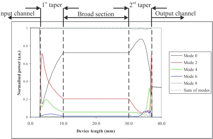
3.5.2 Investigation of Taper Shape and Adiabatic Operation 63 3.5.2.1 Discussion of Results . . . 64
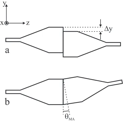
3.5.3 Effect on Performance of Taper End-Face Misalign-ment . . . 69
3.5.3.1 Discussion of Results . . . 70
3.5.4 Three Dimensional Analysis . . . 73
3.5.4.1 Discussion of Results . . . 74
3.6 Summary . . . 77
3.7 References . . . 78
4 Tapered Waveguides fabricated by Thermal Ion Exchange 82 4.1 Introduction . . . 82
4.2 Thermal Ion Exchange from a Molten Salt . . . 82
4.3 Diffusion Theory . . . 90
4.3.1 One Dimensional Solution of the Diffusion Equation 91 4.3.2 Two Dimensional Solution of the Diffusion Equation 93 4.4 Fabrication . . . 94
4.4.1 Sample Preparation . . . 94
4.4.2 Deposition of an Ion Exchange Mask . . . 95
4.4.3 Photolithography . . . 96
4.4.4 Production of Waveguides by TIE . . . 97
4.4.5 Fabrication of TIE Waveguides in IOG-1 Glass . . . . 98
4.5 Direct Characterisation . . . 100
4.5.1 Discussion of SIMS analysis . . . 102
4.6 Optical Characterisation of TIE Waveguides . . . 104
4.6.1 Preliminary investigation of a Tapered Waveguide . . 105
4.6.2 Comparison of Parabolic and Linear Tapers . . . 110
4.6.3 Waveguides in Ytterbium doped IOG-1 . . . 113
4.6.4 Tapered Waveguides in Hybrid BK7 . . . 116
4.6.5 Diode pumping of Tapered Waveguides . . . 118
4.7 Summary . . . 122
4.8 References . . . 123
5 Tapered Waveguides fabricated by Field Assisted Ion Exchange 127 5.1 Introduction . . . 127
5.2 Improvement of Pump and Laser Overlap with FAIE . . . . 128
5.2.1 Pump and Laser Overlap . . . 129
5.3 FAIE Diffusion Theory . . . 133
5.4 Practicalities of the FAIE Process . . . 136
5.5 Fabrication of FAIE Waveguides . . . 139
5.6 Direct Characterisation of FAIE by SIMS . . . 141
5.6.1 SIMS Fitting Results and Discussion . . . 142
5.7 Optical Characterisation of FAIE Waveguides . . . 145
5.7.1 Determination of Waveguide Depth . . . 145
5.7.2 The Prism Coupler . . . 146
5.9 References . . . 153
6 Indiffused Waveguides in Yttrium Vanadate 156 6.1 Introduction . . . 156
6.2 Indiffusion: Historical Summary . . . 157
6.3 Indiffusion Theory . . . 158
6.3.1 Solution to the One-dimensional Indiffusion Equation160 6.3.1.1 Solution to the Indiffusion Equation for an Unlimited Source . . . 160
6.3.1.2 Solution to the Indiffusion Equation for an Instantaneously Depleted Source . . . 161
6.4 High Power Tapered Waveguides . . . 162
6.4.1 Material Requirements of Diode-pumped, Tapered Waveguide Lasers . . . 163
6.4.2 Side-pumping of a Tapered Waveguide . . . 164
6.4.3 Yttrium Vanadate as a Material for High Power, In-diffused Waveguides. . . 167
6.5 Fabrication . . . 169
6.5.1 Sample Preparation . . . 169
6.5.2 Deposition of a Diffusant Metal Layer . . . 170
6.5.3 Indiffusion . . . 172
6.6 Characterisation . . . 174
6.6.1 Surface Defects . . . 174
6.6.2 SIMS Analysis . . . 175
6.6.3 Calibration of SIMS data . . . 176
6.6.4 Fitting of SIMS data to Theoretical Profiles . . . 177
6.6.5 Calculation of Diffusion Properties . . . 180
6.6.6 Discussion of SIMS Results . . . 181
6.6.7 Fluorescence Spectroscopy . . . 184
6.6.8 Investigation of Waveguide Modes . . . 186
6.7 Summary . . . 187
7.2 Tapered Waveguides fabricated by Thermal Ion Exchange . 194 7.3 Tapered Waveguides fabricated by Field-Assisted Ion
Ex-change . . . 197 7.4 Indiffused Waveguides in Yttrium Vanadate . . . 198 7.5 References . . . 200
A The Effective Index Method 202 A.0.1 Propagation Angle in a Channel Waveguide . . . 204 A.1 References . . . 205
B Taper Design Features of Photolithographic Masks 207
C Derivation of the Non-Linear Diffusion Equation 210 C.1 References . . . 212
D List of Publications 213
Introduction
1.1 Diode-pumped Solid-State Lasers
Solid-state lasers have been the focus of a great deal of research since the realisation of the first laser in 1960 [1]. The solid-state lasers detailed in this thesis consist of a host material, either a crystal or glass, doped with an ac-tive ion. Both semiconductor lasers and the relaac-tively new ceramic based lasers [2] are also classified within the solid-state laser group, however, the scope of this thesis is limited to diode-pumped solid-state glass and crystal lasers. An extensive number of active ions have been studied, the majority of which belong to the rare-earth (RE) or transition metal groups, allow-ing access to a wavelength range that spans from the ultraviolet to the mid-infrared. This vast wavelength range has allowed solid-state lasers to find applications within such diverse fields as medicine, materials process-ing, range-finding and research. Host materials have also been extensively studied, with hundreds of possible hosts presently available [3].
Early diode-lasers suffered from limited output powers, and are still lim-ited to powers of ≈ 10W for an individual diode emitter [7, 8]. However, far greater power can be accessed through the use of diode-bars, although this increase in power is accompanied by an increase in the beam asym-metry and a reduction in the beam quality. Therefore, the benefits of a diode-laser pump have to be offset against the difficulties involved with efficiently coupling the highly asymmetric and multimode pump beam into a solid-state gain medium. Various solutions have been proposed for coupling into bulk media such as: shaping the beam [9], the use of re-flective pump chambers [10, 11], lens ducts [12] and fibre coupling [13]. With the exception of reflective pump chambers, these solutions attempt to improve the geometrical match of the diode-laser output with the bulk-laser mode, and rely on manipulating the diode-bulk-laser output. An alterna-tive approach is to design a laser gain medium that naturally provides a geometrical match with the output from a diode-laser. The planar waveg-uide is such a structure; it is inherently well matched to the diode-laser output, allowing a reduction in the pump coupling optics required [14], or in some cases, requiring no coupling optics at all [15].
1.2 The Waveguide Geometry
There are a number of possible waveguide geometries, all of which op-erate by confining optical radiation within the waveguide core through the use of total internal reflection. Examples of the main geometries are depicted in figure 1.1.
suscepti-a
b
c
d
n3
n2
n2
n2 n2
n3
n3 n3
Core Cladding
Substrate
Superstrate
Core
Core
Core
Substrate Substrate
[image:13.595.137.460.102.284.2]n1
Figure 1.1: Main waveguide geometries: a/ Fibre, b/ 3-layer, air-clad planar, c/ 3-layer planar, d/ Channel
bility to vibration, moisture and temperature drift. The slab geometry, of which the planar waveguide is an extreme example, is well known to have superior thermal properties in comparison to the rod geometry [16], and is therefore attractive for reducing thermally induced problems experienced under high pump powers.
Planar fabrication methods, and the planar geometry of the laser itself, are perfectly suited to the production of optoelectronic integrated circuits (OIC’s) [17]. The possibilities of the OIC have been discussed since 1960, with research fuelled by the desire to produce a renaissance in optics sim-ilar to that which accompanied the production of the first electronic inte-grated circuits (IC’s). The development of the OIC has been hampered by the lack of an optical analogue to silicon, and the lack of suitable laser sources [18]. The tapered waveguide laser, investigated in the follow-ing chapters, fulfils the requirements of such a device with early research showing reasonable output power, efficiency and near-symmetric, single transverse mode operation.
1.2.1 Waveguide Lasers
in the fabrication of optical glasses have resulted in the production of ex-tremely low-loss fibres (< 0.1dBkm−1), which are attractive laser hosts.
Although the fibre geometry is not inherently suited to diode-laser pump-ing, the innovation of double-clad fibres [20, 21] has led to output powers up to110W with near-diffraction limited output [22], and272W with only a slightly reduced beam quality [23].
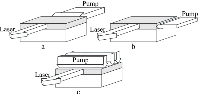
In comparison to fibre lasers, planar waveguides benefit from a geometri-cal match to the output of a diode-laser and fabrication is possible within many different host materials. There is also a greater degree of versa-tility concerning the pump arrangement, with three separate geometries possible. In the end-pumped geometry (figure 1.2a), both the laser and pump propagate co-linearly, allowing the greatest overlap between pump and laser modes [25], although scaling to higher powers is limited by the use of a single pump source. Side-pumping (figure 1.2b), in which the pump and laser propagate perpendicularly, suffers from a reduced pump and laser overlap, which can lead to a lower efficiency in comparison to end-pumping. A significant advantage of the side-pumped geometry is that simple power scaling can be achieved by increasing the length over which the waveguide is pumped to allow more pump units, or by pump-ing both side faces [26]. Face pumppump-ing (figure 1.2c) also has the potential for power scaling, as the large area of the top face can be pumped with stacked diode bars [27]. However, relatively large core depths and reflec-tive pump chambers are required for efficient absorption.
RE doped, planar waveguide lasers were first realised in 1972 [24], but suffered from a high threshold power and required cooling to 77K. Two decades elapsed before the advent of the first high-power diode-side-pumped waveguide laser, which consisted of a Nd3+-doped yttrium
re-Laser
Pump
Pump
Laser
Laser
Pump
a b
[image:15.595.136.462.104.257.2]c
Figure 1.2: Pump geometries: a/ End-pumping, b/ Side-pumping, c/ Face-pumping
quires a hybrid unstable-stable resonator to improve the beam quality.
It would be desirable to obtain both high output power and diffraction limited performance from a monolithic laser design. These specifications restrict waveguide design, as efficient pump coupling requires a multi-mode waveguide, whereas diffraction limited performance requires single-mode laser operation. One method is the use of double-clad planar waveg-uides, which have led to output powers of>10W for Tm3+[26], Yb3+[30]
and Nd3+-doped YAG [30]. However, diffraction limited performance is
only achieved in the guided axis of the waveguide.
1.2.2 The Tapered Waveguide Laser
A different approach is required to attain the goal of diffraction-limited operation in both axes, combined with a monolithic design and access to reasonably high pump powers. The most straightforward technique is to focus the pump beam to match the fundamental laser mode. The beam waist ω0 in a stable laser cavity can be calculated with reference to the
following equation [31]:
ω0 =
µ
Lλ π
¶1 2 · g
1g2(1−g1g2)
(g1+g2−2g1g2)2
¸1 4
WhereLis the cavity length,λis the wavelength within the gain material, g1,2 = 1−L/R1,2 andR1,2is the curvature of the end-face mirrors.
A near-planar, monolithic cavity of a few centimetres in length, lasing at
≈ 1µm, would lead to a beam waist size in the order of a 100µm, which limits pumping to sources that can be efficiently focussed to this degree. Alternatively, the high gain afforded by the waveguide geometry allows the use of a hybrid unstable/stable resonator to improve the non-guided beam quality of a planar waveguide, with a recent non-monolithic device shown to operate successfully [32]. A monolithic design has also been pro-duced, through the fabrication-intensive procedure of polishing curved waveguide end-faces, but this prototype requires further optimisation be-fore successful operation can be attained [33]. Diffraction limited output in both directions can be achieved through the use of a channel structure, although this geometry is not well suited to high-power diode-pumping. Output powers of only 1W [34] have been demonstrated, and an external cavity was required to achieve diffraction-limited output.
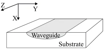
An alternative solution is to combine both the planar and channel geome-tries, in an attempt to gain the benefits of both. The resulting geometry is that of the tapered waveguide, which is depicted in figures 1.3 and 1.4. The tapered waveguide consists of a broad section to allow efficient coupling of a diode-laser, a channel waveguide to select single mode operation and an interconnecting adiabatic taper. The taper allows conversion of the sin-gle laser mode within the channel section, to a sinsin-gle mode of greater lat-eral size within the broad section. Any higher order modes excited during the mode size conversion would be radiated from the waveguide as the mode returned to the channel section. A fundamental requirement for low-loss taper operation, is that the taper maintains all power within the single-mode during the mode size conversion. Operation of this nature is termed ‘adiabatic operation’ and is possible through careful taper de-sign [35, 36].
Broad Section
Taper
Channel section
x y
z n2
n3
n > n2 3
Figure 1.3: 3D view of a tapered waveguide
Broad section Taper Channel section
n
2n > n
2 3n
3Figure 1.4: Plan view of a tapered waveguide
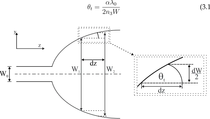
L= W2n3 2αλ0
(1.2)
Where L is the taper length, W is the taper width, n3 is the refractive
in-dex of the substrate and λ0 is the free-space wavelength. The coefficient αcontrols the rate at which the taper opens, and is therefore linked to the adiabatic performance of the taper. Milton and Burns reccomend anα61
for adiabatic taper performance [35]. For reasons that will be explained in section 3.3, equation 1.2 is only applicable to waveguides fabricated with a small difference between the refractive index of the core and the sub-strate (typically 10−3), such as the tapered waveguides produced during
this thesis.
vastly different channel widths would require a taper length of ≈ 20m, which is impractical due to limits on substrate size, fabrication capabilities and propagation losses. However, a broad section width of≈ 200–300µm could be adiabatically converted over a length of≈ 2–3cm, which would allow end-pumping with a single emitter broad-stripe diode, and access to pump powers up to 4W. The first ion-exchanged tapered waveguide laser is demonstrated in chapter 4, early results of diode pumping are also discussed in this chapter. Side-pumping of the broad section with a diode-bar may be possible if the waveguide is fabricated in a material with an absorption coefficient of sufficient magnitude to absorb the pump power over the width of the broad section. The material requirements and the possibilities of this pump geometry are discussed in more detail in chapter 6.
1.3 Solid-State Materials
The work described in the following chapters concerns the laser operation of two ions: neodymium and ytterbium, within two different glass hosts: BK7, a popular silicate glass for optical applications and IOG-1, a relatively new phosphate glass. Initial steps towards the fabrication of a neodymium doped yttrium vanadate laser are also described.
1.3.1 Active Ions
The laser operation of neodymium (Nd) and ytterbium (Yb) doped waveg-uides are studied during this thesis. The relevant energy levels of these ions are depicted in figure 1.5. Rare earth ions have the advantageous property that the 4f electrons, utilised during lasing, are shielded from the crystal field by the filled, outer-lying5sand5pelectron shells [3]. The effect of this shielding is to produce relatively narrow emission lines, and allows the absorption and emission characteristics of the ion to be rela-tively unaffected by doping in different hosts.
1.06 mm
1.8mm
0.94mm
1.3mm
Pump 808nm
4 F3/2 4
F +5/2 2 H9/2 4 I15/2 4 I11/2 4 I13/2 4 I9/2 Non-radiative decay
1.03mm
2 F5/2 2 F7/2 Non-radiative decay Pump 940nm / 970nm
}
a
b
Figure 1.5: Relevant energy levels of a/ neodymium, and b/ ytterbium laser ions
manifold, followed by fast non-radiative decay to one of the Stark split levels of the 4F
3/2 manifold. The strongest transition, from the 4F3/2 to
the 4I
11/2 manifold, results in an emission wavelength of λ ≈ 1.06µm.
The laser operation of the Nd3+ ion is four-level in nature, as the 4I 11/2
manifold is high above the ground state and is therefore unpopulated at room temperature. Apart from the transition to the4I
11/2 manifold, other
weaker transitions are also possible to the4I
15/2,4I13/2and4I9/2manifolds,
resulting in emission wavelengths ofλ ≈1.8µm,λ≈1.3µmandλ≈0.9µm respectively.
Initial research into the laser operation of the Yb3+ion was limited by the
difficulties involved with flashlamp pumping at the required wavelength of ≈ 0.94µm or 0.97µm [37]. The advent of diode-lasers that could effi-ciently pump at these wavelengths renewed interest in the Yb3+ ion, as
it exhibits some attractive features for high power lasers [38]. The small quantum defect between the pump and the ≈ 1.03µm laser wavelength results in reduced thermal loading of the host material, and allows higher output powers to be gained for a given pump power. The Yb3+ ion
dis-plays no higher lying or intermediate manifolds, which eliminates the concentration dependent effects suffered by Nd3+ systems [39], allowing
higher Yb3+ concentrations to be utilised in order to improve the laser
split levels of the 2F
7/2 ground state manifold, which is thermally
popu-lated at room temperature. The resulting quasi-three level operation of an Yb3+laser suffers from re-absorption loss leading to a higher threshold
than that of four-level systems.
1.3.2 Host Materials
Laser hosts can be split into two main categories: glasses and crystals. Glasses have a number of favorable properties which include low cost, large substrate size, high homogeneity, chemical durability, doping flexi-bility and an index match with optical fibres [40]. In comparison to crystal hosts, glasses suffer from lower thermal conductivity, which limits their high power operation, and emission broadening. However, a reason for the continued use of glass in waveguide applications is its compatibility with the ion exchange fabrication technique, which allows simple and re-producible waveguide production. Chapters 4 and 5 deal with the pro-duction of glass waveguides by ion exchange.
In comparison to glasses, crystal hosts are known to possess superior me-chanical strength, thermal conductivity and benefit from a narrower emis-sion linewidth when doped with active ions, however, the cost, doping flexibility and substrate size is often poor in comparison. Yttrium alu-minium garnet (YAG) has achieved a position of dominance for high power applications, due to the ability to dope with Nd3+ and Yb3+ ions and its
very high thermal conductivity and mechanical strength. However, YAG is not a suitable host for the side-pumping of relatively narrow waveg-uides, as will be considered in chapter 6, due to a typical absorption length of a few millimetres for diode-pump sources. In comparison to Nd:YAG, Nd3+-doped yttrium vanadate (Nd:YVO
4) benefits from an absorption
co-efficient ≈ 3×greater, a broader absorption band and a stimulated emis-sion cross-section≈ 6×greater [41, 42]. These properties are very attrac-tive to the diode-side-pumping of the relaattrac-tively narrow waveguides dis-cussed in the previous section. Chapter 6 discusses the possibilities of diode-side-pumping Nd:YVO4 waveguides and details the first
YVO4 is limited by its thermal conductivity [43], which is approximately
half that of YAG, however, the thermal management of the planar geome-try should go some way to overcoming this shortfall.
1.4 Waveguide Fabrication
A wide variety of fabrication techniques are available for the production of waveguides, which can be separated into two groups: layer alteration, which involves the alteration of the upper layer of a substrate and layer deposition, which involves the growth of a new layer on a substrate. Typi-cally the choice of fabrication method is dependant upon the desired prop-erties of the final laser device, i.e. the required host material, waveguide geometry, numerical aperture (NA) and refractive index profile.
Layer alteration techniques often require relatively simple fabrication pro-cedures, are reproducible and cheap to perform. However, as many of these techniques are driven by thermal diffusion they are highly depen-dent on the process temperature, which can result in lengthy fabrication durations [44]. The low refractive index change caused by these tech-niques, and hence the low numerical aperture (NA), is perfectly suited to the production of single mode waveguides, but is not best suited for pumping with non-diffraction limited sources.
of buried waveguides has also been completed using a novel ion exchange technique that involves the contact bonding of a potassium rich glass with a glass of lower potassium concentration [54]. This process benefits from a single-step fabrication procedure and can be combined with UV writing to produce channel waveguides [55].
Field-assisted ion exchange (FAIE) was developed to allow greater flexi-bility over the index profile, and is especially useful for the production of step-index waveguides [52]. FAIE is identical to TIE, except for the addi-tion of an electric field applied across the sample. The electric field drives the migration of the exchanger ions, with fields of sufficient magnitude allowing the thermal diffusion characteristics of the ion exchange to be overcome [45]. Both TIE and FAIE often result in waveguide propagation losses of60.2dBcm−1 [45].
Proton exchange is strongly related to ion-exchange and involves exchang-ing lithium ions within crystals of lithium niobate (LiNbO3) or lithium
tan-talate (LiTaO3), with H+ions from an acidic solution. The simplicity of the
process, coupled with the low propagation losses of 0.15dBcm−1 [56], has
allowed proton exchange to become one of the two major methods used for waveguide fabrication within these crystals. The alternative method for production of low-loss (6 0.5dBcm−1 [57, 58]) waveguides is the
pro-cess of indiffusion [59,60], which has also been completed in sapphire [61] and most recently within YVO4, as discussed in chapter 6. The process
in-volves applying a metal film to the surface of a crystal substrate, followed by heating of the substrate to temperatures≈ 1000–2000℃. During heat-ing, ions within the metal layer diffuse into the crystal, and alter the crys-tal’s refractive index. The index profile produced by indiffusion is graded, with the shape dependant on fabrication parameters [44]. The main bene-fits of the process are the ability to produce waveguides in crystal media, selective doping with active ions, and the possible use of the diffusant ion as both the index modifier and the active ion [62].
of ion exchange and proton exchange, the shielding is completed using a thick layer of metal with features delineated through photolithography and etching. Patterning of the metal source, through the use of a pho-tolithographic lift-off technique, is used to delineate features for indiffu-sion. The simplicity involved with the production of channel waveguides by ion exchange and indiffusion led to their use for the fabrication of ta-pered waveguides during this thesis.
UV writing is a relatively new technique for the fabrication of channel waveguides in glass, which relies on the photosensitivity of various glasses to UV radiation. A UV laser is focussed into the glass substrate and in-duces a refractive index change. Channel waveguides are fabricated by scanning the substrate through the use of a computer controlled transla-tion stage. The main benefit of this method is the flexibility of the waveg-uide geometries that can be fabricated, without the necessity of lengthy photolithographic procedures [64]. The process is suited to the production of low-loss waveguides (< 0.2dBcm−1 [65]), however, as with the other
layer alteration processes discussed here, the refractive index change due to this process is low (∆n ≈ 10−3 [63]) leading to the production of low
NA waveguides.
a tapered waveguide laser using a double-clad design [15], with the extra layers grown through the use of a layer deposition process.
Various layer deposition methods are available such as: liquid phase epi-taxy (LPE) [67,68], molecular beam epiepi-taxy (MBE) [69], pulsed laser depo-sition (PLD) [70], Sol-Gel [71] and flame hydrolysis depodepo-sition (FHD) [72]. One technique that is inherently well matched to the production of high NA, double-clad waveguides is contact (also referred to as thermal or di-rect) bonding. This process involves the high-quality polishing of a core and substrate material, which are chemically cleaned and contacted to-gether. Van der Waals forces bond the two materials with a sufficient bond strength to allow mechanical thinning of the core to the required depth [73]. The process can be repeated to cap the core with a superstrate material, or to produce double-clad devices [15]. Contact bonding is an extremely flexible technique, as no lattice match is required between the two materials, however, it is preferable for the materials to share a similar thermal expansion coefficient to inhibit fracture under high power opera-tion. The flexibility in the choice of the materials allows dissimilar material such as Nd:YAG and glass to be bonded, resulting in a very high NA of 0.8 [73]. As no alteration of the material is required during contact bond-ing, the spectral properties are identical to that of bulk materials and very low-loss waveguides (0.2dBcm−1[14]) can be produced.
1.5 Synopsis
The remainder of this thesis is separated into five chapters, which are or-ganised in the following manner.
later chapters.
An overview of the tapered waveguide and the theory of their operation is discussed in chapter 3. Requirements for the design of tapered waveg-uides are detailed, followed by the analysis of a variety of tapered struc-tures using the beam propagation method (BPM).
The theory, practical requirements and fabrication of thermal ion ex-changed waveguides are detailed in chapter 4. The operation of tapered and channel waveguide lasers are detailed under titanium sapphire and broad-stripe diode-laser pumping. Chapter 5 investigates the possibili-ties of field-assisted ion exchange, with special focus on the production of step-index waveguides.
An initial investigation of indiffusion in YVO4 is detailed in chapter 6,
fol-lowed by a discussion of the theory and practicalities required for the pro-duction of high power diode-side-pumped tapered waveguides. The fab-rication and analysis of planar diffused YVO4 waveguides is completed,
and conclusions are drawn concerning the future of this research.
The final chapter includes the conclusions to the work presented in this thesis, followed by the possibilities for future research.
1.6 Aims and Objectives
1.6.1 Ion Exchanged Tapered Waveguide Lasers
The principle aim in the production of a tapered waveguide laser, using the ion exchange fabrication method in glass, is the production of a 1W -class laser. The tapered waveguide will be designed to be compatible with diode-end-pumping, whilst producing a diffraction-limited output beam.
A tapered waveguide laser, fabricated in Nd3+-doped BK7, can be
as-sumed to operate with a slope efficiency of ≈ 50%. Under this condition, an incident diode-pump power of≈4W would be required to achieve an
Diode name Model no. Output Power M2
(at 808nm)
W (slow axis/fast axis)
Diode A 382D-1330E-3-1 4 39×3.2
Diode B 462D-1375E-3-1 2 22×1.9
Table 1.1: Characteristics of the broad-stripe diode-pump sources used for end-pumping the ion exchanged tapered waveguide laser
The diode-pump beam quality, measured by the M2 value, is
fundamen-tal to achieving a reasonable launch efficiency, and can be related to the numerical aperture NA, and size D of the waveguide by the following equation:
M2 = D×NA
λ (1.3)
The maximum M2 of the diode-pump beam, required to attain
reason-able launch efficiency, can be calculated by entering values for the NA achieved by the potassium/sodium ion exchange technique in BK7 glass, as used throughout this thesis, and the minimum taper width of200µm, as discussed in section 1.2.2. It can be seen that a maximum allowable diode pumpM2 of≈40is required in the width of the tapered waveguide. The
depth of the waveguide is determined by the ion exchange technique, with a depth of ≈ 10µm achievable in reasonable process times. Use of equa-tion 1.3 withD= 10µmproduces a maximum allowable diode-pumpM2
of≈2, in the depth of the waveguide.
Two broad-stripe diode-lasers were purchased from the supplier, Polaroid, under this rationale. The properties of these diode-lasers conform with the requirements discussed in the previous paragraph and are listed in table 1.1.
device, whilst allowing access to output powers of0.5–1W.
The main benefit of the tapered waveguide design is the relatively straight-forward method of producing a diffraction-limited output. Tailoring the physical size of the channel section of the tapered waveguide, so that only a single transverse mode is supported in both the depth and width of the channel, should allow near-diffraction-limited output. Theoretically, an output beam quality with anM2 ≈1could be attained.
1.6.2 Indiffused Waveguides in Yttrium Vanadate
As discussed in section 1.3.2, it may be possible to diode-side-pump the broad section of a tapered waveguide laser. In relation to end-pumping, the side-pump arrangement allows a lower diode-pump, slow-axis beam quality to be launched into the waveguide. The broad section of the ta-pered waveguide can be fabricated with any desired length, and is limited only by the substrate size and fabrication constraints. The relatively small substrate size available would limit the broad section length to ≈ 10mm. Use of equation 1.3 with D = 10mm, assuming an identical NA to that of the ion exchange process, sets a maximum limit on the lateral diode-pump beam quality of M2 ≈ 2000. However, it is reasonable to assume
that the beam quality in the depth of the waveguide would still be limited toM2 ≈2. Diode-bars with output powers in the order of50W are
avail-able with an M2 approximately equal to these requirements. Diode-bar
side-pumping of a tapered waveguide at a power of ≈ 50W may allow access to an output laser power of ≈ 10W, in a near-diffraction-limited beam.
The relatively narrow taper widths of 200–300µm, obtained over a rea-sonable substrate length, would require the tapered waveguide to be pro-duced in a material with a high pump absorption coefficient. Yttrium vanadate (YVO4), doped with1at%Nd3+, benefits from a maximum
ab-sorption coefficient of 37cm−1, for light polarised parallel to the crystal
possi-ble to absorb a fraction of at least1/eof the launched diode-power, which theoretically, may allow the production of an efficient diode-side-pumped tapered waveguide laser.
Local doping of the laser ion is required for efficient side-pumping. The process of indiffusion would allow both local doping with the laser ions, and the production of a waveguide in the YVO4 crystal host. However,
indiffusion in YVO4 has not been studied and, for this reason, the first aim
of this section is the determination of the diffusion characteristics of the Nd3+ ion in YVO
4. Calculation of the diffusion coefficient of the Nd3+
ion, would allow the design and fabrication of waveguides with a suitable doping concentration and waveguide depth, for the production of tapered waveguide lasers. The diffusion characteristics of Gd3+ and Tix+will also
be investigated, as these ions may prove to be suitable for index modifica-tion, which would allow flexibility over the design of the index and gain profiles.
To highlight the applicability of the indiffusion technique, it is also desir-able to produce the first indiffused waveguide in YVO4. Once this first
waveguide has been produced, determination of the waveguide proper-ties would allow later waveguides to be designed with specific waveguide properties. It would be desirable to produce a waveguide that supports a single mode at the Nd3+ laser wavelength, however, this may not be
pos-sible at this early stage.
1.7 References
[1] T. Maiman. Stimulated Optical Radiation in Ruby. Nature, 187 : p493– 494, 1960.
[2] J.H Lu, J.R. Lu, T. Murai, K. Takaichi, T. Uematsu, J.Q. Xu, K. Ueda, H. Yagi, T. Yanagitani, A.A. Kaminskii. 36-W diode-pumped continuous-wave 1319-nm Nd : YAG ceramic laser. OL, 27(13) : p1120–1122, 2002.
[4] R.L. Byer. Diode Laser-Pumped Solid-State Lasers. Science, 239 : p742– 747, 1988.
[5] R.D. Dupuis. An Introduction to the Development of the Semiconduc-tor Laser. IEEE Journal of Quantum Electronics, QE-23(6) : p651–657, 1987.
[6] R.J. Keyes and T.M. Quist. Injection luminescent pumping of CaF2:U3+
with GaAs Diode Lasers. Applied Physics Letters, 4(3) : p50–52, 1964.
[7] J. Sebastian, G. Beister, F. Bugge, F. Buhrandt, G. Erbert, H.G. Hansel, R. hulsewede, A. Knauer, W. Pittroff, R. Staske, M. Schroder, H. Wen-zel, M. Weyers and G. Trankle. High-Power 810nm GaAsP-AlGaAs Diode Lasers with Narrow Beam Divergence. IEEE Journal on Selected Topics in Quantum Electronics, 7(2) : p334–338, 2001.
[8] A. Al-Muhanna, L.J. Mawst, D. Botez, D.Z. Garbuzov, R.U. Martinelli and J.C. Connolly. High-Power (> 10W) continuous-wave operation from 100-µm-aperture 0.97-µm-emitting Al-free diode lasers. Applied Physics Letters, 73(9) : p1182–1184, 1998.
[9] W.A. Clarkson and D.C. Hanna. Two-mirror beam-shaping technique for high-power diode-bars. Optics Letters, 21(6) : p375–377, 1996.
[10] D.V. Pantelic, B.M. Panic and L. Belic. Solid-state laser pumping with a planar compound parabolic concentrator. Applied Optics, 36(30) : p7730–7740, 1997.
[11] Y. Wang, I. Hirano and H. Kan. Theoretical study on absorption effi-ciency for a LD side-pumped Nd:YAG laser with infinite convergence approach. Infrared Physics and Technology, 44(3) : p213–225, 2002.
[12] R.J. Beach. Theory and optimization of lens ducts. Applied Optics, 35(12) : p2005–2015, 1996.
[14] D.P. Shepherd, C.L. Bonner, C.T.A. Brown, W.A. Clarkson, A.C. Trop-per, D.C. Hanna and H.E. Meissner. High-numerical-aperture, contact-bonded, planar waveguides for diode-bar-pumped lasers.Optics Com-munications, 160 : p47–50, 1999.
[15] C.L. Bonner, T. Bhutta, D.P. Shepherd and A.C. Tropper. Double-Clad Structures and Proximity Coupling for Diode-Bar-Pumped Pla-nar Waveguide Lasers. IEEE Journal of Quantum Electronics, 36(2) : p236–242, 2000.
[16] J.M. Eggleston, T.J. Kan, K. Kuhn, J. Unternahrer and R.L. Byer. The Slab Geomtery – Part 1: Theory. IEEE Journal of Quantum Electronics, QE-20(3) : p289–301, 1984.
[17] S.I. Najafi. Introduction to Glass Integrated Optics. Artech House, Ch. 1, Norwood, 1992.
[18] R.G. Hunsperger. Integrated Optics: Theory and Technology.Springer Verlag, Ch. 1, Berlin, 1985.
[19] E. Snitzer. Optical Maser Action of Nd3+ in a Barium Crown Glass.
Physical Review Letters, 7(12) : p444–446, 1961.
[20] G. Bouwmans, R.M. Percival, W.J. Wadsworth, J.C. Knight and P. St. J. Russell. High-power Er:Yb fiber laser with very high numerical aper-ture pump-cladding waveguide. Applied Physics Letters, 83(5) : p817– 818, 2003.
[21] M. Hofer, M.E. Fermann and L. Goldberg. High-Power Side-Pumped Passively Mode-locked Er-Yb Fiber Laser. IEEE Photonics Technology Letters, 10(9) : p1247–1249, 1998.
[22] V. Dominic, S. MacCormack, R. Waarts, S. Sanders, S. Bicknese, R. Dohle, E. Wolak, P.S. Yeh and E. Zucker. 110W fibre laser. Electronics Letters, 35 : p1158–1160, 1999.
[24] J.P. Van der Ziel, W.A. Bonner and L.G. Van Uitert. Coherent Emission from Ho3+ Ions in Epitaxially Grown Thin Aluminium Garnet Films.
Physics Letters, 42A(1) : p105–106, 1972.
[25] C.L. Bonner, C.T.A. Brown, D.P. Shepherd, W.A. Clarkson, A.C. Tropper and D.C. Hanna. Diode-bar end-pumped high-power Nd:Y3Al5O12planar waveguide laser.Optics Letters, 23(12) : p942–944,
1998.
[26] J.I. Mackenzie, S.C. Mitchell, R.J. Beach, H.E. Meissner and D.P. Shep-herd. 15W diode-side-pumped Tm:YAG waveguide laser at2µm. Elec-tronics Letters, 37(14) : p898–899, 2001.
[27] A. Faulstich, H.J. Baker and D.R. Hall. Face pumping of thin, solid-state slab lasers with laser diodes.Optics Letters, 21(5) : p594–596, 1996.
[28] D.C. Hanna, A.C. Large, D.P. Shepherd, A.C. Tropper, I. Chartier, B. Ferrnad and D. Pelenc. A side-pumped Nd:YAG epitaxial waveguide laser. Optics Communications, 19 : p229–235, 1992.
[29] J.R. Lee, H.J. Baker, G.J. Friel, G.J. Hilton and D.R. Hall. High-average-power Nd:YAG planar waveguide laser that is face pumped by 10 laser diode bars. Optics Letters, 27(7) : p524–526, 2002.
[30] R.J. Beach, S.C. Mitchell, H.E. Meissner, O.R. Meissner, W.F. Krupke, J.M. McMahon and W.J. Bennet. Continuous-wave and passively Q-switched cladding-pumped planar waveguide lasers. Optics Letters, 26(12) : p881–883, 2001.
[31] O. Svelto. Principles of Lasers. Plenum Press, New York, Fourth Edi-tion, Ch.5, 1998.
[32] H.J. Baker, A.A. Chesworth, D.P. Millas and D.R. Hall. A pla-nar waveguide Nd:YAG laser with a hybrid waveguide-unstable res-onator. Optics Communications, 191 : p125–131, 2001.
[33] J.I. Mackenzie. High-Brightness Diode-Pumped Waveguide Lasers.
[34] U. Griebner and H. Sconnagel. Laser operation with nearly diffraction-limited output from a Yb:YAG multimode channel waveg-uide. Optics Letters, 24(11) : p750–752, 1999.
[35] A.F. Milton and W.K. Burns. Mode Coupling in Optical Waveguide Horns.IEEE Journal of Quantum Electronics, QE-13(10) : p828–835, 1977.
[36] I. Duport, P. Benech, D. Khalil and R. Rimet. Study of linear tapered waveguides made by ion exchange in glass. Applied Physics Letters, 82(9) : p1332–1334, 2003.
[37] H.W. Etzel, H.W. Gandy and R.J Gunther. Stimulated Emission of Infrared Radiation from Ytterbium Activated Silicate Glass. Applied Optics, 1(4) : p534–536, 1962.
[38] T.Y. Fan. Solid State Lasers: New Developments and Applications.
Plenum Press, New York, 1993.
[39] S. Guy, C.L. Bonner, D.P. Shepherd, D.C. Hanna, A.C. Tropper and B. Ferrand. High-Inversion Densities in Nd:YAG: Upconversion and Bleaching. IEEE Journal of Quantum Electronics, 34(5) : p900–909, 1998.
[40] N.V. Nikonorov and G.T. Petrovskii. Ion-Exchanged Glasses in In-tegrated Optics: The Current State of Research and Prospects (A Re-view). Glass Physics and Chemistry, 25(1) : p16–54, 1999.
[41] L. DeShazer. Vanadate Crystals exploit diode pump technology.Laser Focus World, 30(2) : p88–93, 1984.
[42] A. Brignon, G. Feugnet, J.P. Huignard and J.P. Pochelle. Compact Nd:YAG and Nd:YVO4Amplifiers End-Pumped by a High-Brightness
Stacked Array. IEEE Journal of Quantum Electronics, 34(3) : p577–585, 1998.
[43] X. Peng, L. Xu and A. Asundi. Power Scaling of Diode-Pumped Nd:YVO4 Lasers. IEEE Journal of Quantum Electronics, 38(9) : p1291–
1299, 2002.
[45] R.V. Ramaswamy and R. Srivastava. Ion-Exchanged Glass Waveg-uides: A Review. Journal of Lightwave Technology, 6(6) : p984–1001, 1987.
[46] T. Izawa and H. Nakagome. Optical waveguide formed by electri-cally induced migration of ions in glass plates. Applied Physics Letters, 21(12) : p584–586, 1972.
[47] G. Giallorenzi, E.J. West, R. Kirk, R. Ginther and R.A. Andrews. Opti-cal Waveguides Formed by Thermal Migration of Ions in Glass.Applied Optics, 12(6) : p1240–1244, 1973.
[48] G.H. Chartier, P. Jassaud, A.D. de Oliveira and O. Parriaux. Fast fab-rication method for thick and highly multimode optical waveguides.
Electronics Letters, 13 : p763–764, 1977.
[49] V. Neuman, O. Parriaux and L.M. Walpita. Double-alkali effect: Influ-ence of index profile of ion-exchanged waveguides. Electronics Letters, 15 : p704–705, 1979.
[50] G.H. Chartier, P. Jassaud, A.D. de Oliveira and O. Parriaux. Opti-cal waveguides fabricated by electric-field controlled ion exchange in glass. Electronics Letters, 14(5) : p132–134, 1978.
[51] S.S. Geveorgyan. Single-step buried waveguides in glass by field-assisted copper ion-exchange. Electronics Letters, 26(1) : p38–39, 1990.
[52] A. Opilski, R. Rogozinski, M. Blahut, P. Karasinski, K. Gut and Z. Opilski. Technology of ion exchange in glass and its application in waveguide planar sensors. Œ, 36(6) : p1625–1638, 1997.
[53] R.V. Ramaswamy and S.I. Najafi. Planar, Buried, Ion-Exchanged Glass Waveguides: Diffusion Characteristics. IEEE Journal of Quantum Electronics, QE-22(6) : p883–891, 1986.
[54] C.B.E. Gawith, T.Bhutta, D.P. Shepherd, P. Hua, J. Wang, G.W. Ross and P.G.R. Smith. Buried laser waveguides in neodymium-doped BK-7 by K+–Na+ ion-exchange across a direct-bonded interface. Applied
[55] T. Bhutta. Novel Rare-Earth-Doped Planar Waveguide Lasers. PhD. Thesis, University of Southampton - Southampton, 2002.
[56] P.G. Suchoski, T.K. Findakly and F.J. Leonberger. Stable low-loss proton-exchanged LiNbO3 waveguide devices with no electro-optic
degradation. Optics Letters, 13(11), p1050–1052, 1988.
[57] J. Amin, M. Hempstead, J.E. Roman and J.S. Wilkinson. Tunable coupled-cavity waveguide laser at room temperature in Nd-diffused Ti:LiNbO3. Optics Letters, 19(19), p1541–1543, 1994.
[58] J.K. Jones, J.P. de Sandro, M. Hempstead, D.P. Shepherd, A.C. Large, A.C. Tropper and J.S. Wilkinson. Channel waveguide laser at1µmin Yb-indiffused LiNbO3. Optics Letters, 20(13) : p1477–1479, 1995.
[59] R.V. Schmidt and I.P. Kaminow. Metal-diffused optical waveguides in LiNbO3. Applied Physics Letters, 25(8) : p458–460, 1974.
[60] I.P. Kaminow and J.R. Carruthers. Optical waveguiding layers in LiNbO3 and LiTaO3. Applied Physics Letters, 22(7) : p326–328, 1973. [61] L.M.B. Hickey and J.S. Wilkinson. Titanium diffused waveguides in
sapphire. Electronics Letters, 32(24) : p2238–2239, 1996.
[62] L.M.B. Hickey. Ti:sapphire waveguide laser by the thermal diffu-sion of Ti into sapphire. PhD. Thesis, University of Southampton -Southampton, 1998.
[63] M. Svalgaard, C.V. Poulsen, A. Bjarklev and O. Poulsen. Direct UV writing of buried singlemode channel waveguides in Ge-doped silica films. Electronics Letters, 30(17) : p1401–1403, 1994.
[64] G.D. Emmerson, S.P. Watts, C.B.E. Gawith, V. Albanis, M. Ibsen, R.B. Williams and P.G.R. Smith. Fabrication of directly UV-written chan-nel waveguides with simultaneously defined integral Bragg gratings.
Electronics Letters, 38(24) : p1531–1532, 2002.
-doped chalcogenide (Ga:La:S) glass through photoinduced material modification. Applied Physics Letters, 81(20) : p3708–3710, 2002.
[66] J.P. Wittke. Thin-Film Lasers. RCA Review, 33 : p674–694, 1972.
[67] D.L. Lee. Electromagnetic Principles of Integrated Optics. J. Wiley & Sons, Ch.7, New York, 1986.
[68] B. Ferrand, B. Chambaz and M. Couchaud. Liquid phase epitaxy: A versatile technique for the development of miniature optical compo-nents in single crystal dielectric media.Optical Materials, 11 : p101–114, 1999.
[69] T. Bhutta, A.M. Chardon, D.P. Shepherd, E. Daran, C. Serrano and A. Munoz-Yague. Low Phonon Energy, Nd:LaF3 Channel Waveguide
Laser Fabricated by Molecular Beam Epitaxy. IEEE Journal of Quantum Electronics, 37(11) : p1469–1477, 2001.
[70] S.J. Barrington. Planar waveguide devices fabricated by pulsed laser deposition. PhD. Thesis, University of Southampton - Southampton, 2001.
[71] R.M. Almeida, P.J. Morais and A.C. Marques. Planar waveguides for integrated optics prepared by sol-gel methods. Philosophical Magazine B, 82(6) : p707–719, 2002.
[72] M. Kawachi, M. Yasu and T. Edahiro. Fabrication of SiO2–TiO2 Glass
Planar Optical Waveguides by Flame Hydrolysis Deposition. Electron-ics Letters, 19(15) : p583–584, 1983.
Waveguide Laser Theory
2.1 Introduction
The following chapter details the two fundamental theories that govern the operation of waveguide lasers: electromagnetic theory and laser the-ory.
Knowledge of the number of propagating modes and their profile is of great importance to waveguide lasers, as the optical confinement offered by the waveguide geometry alters the modes available from those found within bulk lasers. Electromagnetic theory is applied to a planar asym-metric slab waveguide [1], which describes the general operation of the waveguides fabricated during this thesis. The theory is then extended to more accurately model the effects of graded index planar waveguides us-ing the WKB method [2]. Modellus-ing of uniform and graded index planar waveguides is completed to illustrate the effect of the refractive index pro-file on the guided modes.
2.2 Waveguide Modes
2.2.1 Electromagnetic Theory
Maxwell’s equations are the starting point for determining the modal be-haviour within any medium. Within an isotropic, source-free medium the electric (E) and magnetic (H) field vectors are related as follows [5]:
∇ ×E∼ =−µ∂
∂tH∼ (2.1)
∇ ×H∼ =ε∂
∂tE∼ (2.2)
∇ ·E∼ = 0 (2.3)
∇ ·H∼ = 0 (2.4)
Where ∇ is the spatial vector operator, µand ε are the permeability and permittivity of the medium and∂/∂tis the partial derivative with respect to timet.
The equations are simplified by separating the temporal and spatial re-liance of the fields, by assuming a time harmonic relation of the form:
E∼(r∼, t) = E−(∼r)eiωt (2.5)
Where E− is a complex phasor, and describes only the spatial variation of the vector (E∼), ∼ris the position vector (= xxˆ+yyˆ+zzˆ), ω is the angular frequency of the field andi=√−1.
This allows equations 2.1–2.4 to be rewritten as follows:
∇ ×H− =iωεE− (2.7)
∇ ·E− = 0 (2.8)
∇ ·H− = 0 (2.9)
Maxwell’s curl equations (equations 2.6 and 2.7), in conjunction with the vector identity (whereU− is any vector):
∇ ׳∇ ×U−´=∇³∇ ·U−´− ∇2U
− (2.10)
allow the calculation of the homogenous wave equation, which relates the variation of the E-field in spatial and temporal dimensions, and allows calculation of the mode profiles within a waveguide:
∇2E
− +ω
2µεE
− = 0 (2.11)
The concept of duality is used during the following derivations, to reduce the volume of mathematics required. It has been shown [1] that due to the symmetry of Maxwell’s equations, once a solution for one field has been calculated the solution for the other field is found by making the substitutionsE → −H,H →E,µ→εandε→µ.
2.2.2 Solution of the Wave Equation for an Asymmetric
Waveguide
x
z
Region 1: superstrate
Region 2: core
Region 3: substrate
e , m1 1
e , m3 3 e , m2 2
x = d/2
x = -d/2
x = 0
y
Figure 2.1: The asymmetric waveguide
generally applicable to all three layer waveguides and are readily con-verted to those required for the symmetric slab waveguide.
The asymmetric slab waveguide, which is assumed to extend infinitely in theyandz directions (figure 2.1), consists of three distinct regions:
1. The superstrate, which is often the surrounding atmosphere and is characterised byε1,µ1
2. The core, characterised byε2,µ2and depth=d 3. The substrate, characterised byε3,µ3
It is often more practical to refer to the refractive index of the waveg-uide regions, which is calculated via the permittivity of the region: nm = p
εm/ε0, whereε0is the permittivity of free-space andmdenotes the
waveg-uide region. For guidance to occur the indices of the three regions must be chosen so thatn2 > n1, n3. The numerical apertureNAis also an important
quantity when discussing waveguides, and is defined:
NA = sinθ= q
n2
2 −n21 (2.12)
The boundary between the core and superstrate or substrate, negates TEM mode propagation within a waveguide structure [6]. Instead, there are two allowed polarisation states: transverse electric (TE) where the electric field is polarised in they-direction (Ex = Ez = 0, Hz 6= 0) and transverse
magnetic (TM) where the magnetic field is polarised in the y-direction (Hx = Hz = 0, Ez 6= 0). The quantities Ex, Ey, Ez, Hx, Hy, Hz are the
projection of the complex phasors E− and H− onto the x, y and z axes re-spectively, and therefore do not require the under-bars in their notation.
2.2.2.1 TE Mode Solutions
The fields within the superstrate and substrate are assumed to decay expo-nentially with increasing distance from the core in the x-direction. Within the core the fields are assumed to have a standing-wave nature in the x -direction, and therefore to be oscillatory in nature. In the direction of prop-agation (z-direction) the fields are assumed to have a common wavevector, allowing the field solution to be expressed:
E∼(r∼, t) = E−(∼r)eiωte−ikzz =E
−(r∼)e
i(ωt−kzz) (2.13)
Wherekz is the wave vector in the z-direction.
Based upon the above assumptions, the proposed TE solutions are as fol-lows:
Ey(x, z) =
A1e−α1x
A2cos (kxx+ Ψ)
A3e−α3x
e−ikzz
x > d/2
d/2>x>−d/2
x <−d/2
(2.14)
Where A1–A3 are the amplitude coefficients to the solutions in each
re-gion of the waveguide, α1 and α3 are the decay coefficients in regions 1
Substituting each of the components of equation 2.14 into equation 2.11, allows calculation of the coefficients α1, α3 and kx that satisfy the wave
equation. These equations are named the dispersion relations and are of the form:
α1 =
p
k2
z−ω2µ1ε1 (2.15)
α3 =
p
k2
z−ω2µ3ε3 (2.16)
kx = p
ω2µ
2ε2−k2z (2.17)
It is a physical requirement that the E and H-fields must be continuous across the interfaces atx = d/2,−d/2. This is equivalent to requiring the tangential components of the fields to be equal at the interface. The tan-gential H-field is determined from Maxwell’s curl equations:
Hz(x, z) =
i ωµm
∂
∂xEy(x, z) (2.18)
The above equation is used to derive the z-component of the H-field within each region of the waveguide:
Hz(x, z) = −iα1
ωµ1 A1e−α1x
−ik2
ωµ2A2cos (kxx+ Ψ) iα3
ωµ3A3e−α3x
e−ikzz
x > d/2
d/2>x>−d/2
x <−d/2
(2.19)
The tangential fields for the interface atx=d/2are as follows:
Etan : A1e−
α1d
2 =A2cos µ
kxd 2 + Ψ
(2.20)
Htan :
−iα1 ωµ1
A1e−
α1d
2 = −ikx
ωµ2
A2sin
µ
kxd 2 + Ψ
Equation 2.14 can now be simplified using equation 2.20 to state the coeffi-cientA1in terms ofA2. SimilarlyA3can be stated in terms ofA2by
manip-ulation of the tangential components atx = −d/2. The field components within each region can now be stated in relation to only the magnitude of the field component within the core:
Ey(x, z) = A2
cos¡kxd
2 + Ψ
¢
e−α1(x−d/2)
cos (kxx+ Ψ) cos¡kxd
2 −Ψ
¢
eα3(x+d/2)
e−ikzz
x > d/2
d/2>x>−d/2
x <−d/2
(2.22)
The guidance condition for the mode atx=d/2is found by dividing 2.21 by 2.20, and after some manipulation this is stated as follows:
kxd
2 + Ψ = tan
−1
µ
µ2α1 µ1kx
(2.23)
And atx=−d/2:
kxd
2 −Ψ = tan
−1
µ
µ2α3 µ3kx
(2.24)
These guidance conditions are combined additively to remove theΨterm to produce the full guidance condition:
2kxd−ϕT E1 −ϕT E3 = 2pπ (2.25)
Wherep= 0,1,2, ...is the mode number and:
ϕT Em = 2 tan−1 µ
µ2αm
µmkx 
(2.26)
Wheremdenotes either region1or3.
The terms ϕ1 and ϕ3 are the phase changes due to reflection at the
su-perstrate/core and core/substrate interfaces, whereas the term2kxdis the
condition can be physically explained as a statement that the net phase change of a guided mode over one round-trip within the core, must equal an integer multiple of2π.
X-direction
Int
ens
it
y
(a
.u.)
d / 2 -d / 2 0
l=l 0 l= 2l
0 l= 3l
0
Figure 2.2: TE guided mode profile of fundamental mode for arbitraryλ0
X-direction
Int
ens
it
y
(a
.u.)
d / 2
-d / 2 0
l= 3l
0
l= 2l
0
l=l
0
Figure 2.3: TE guided mode profile of first higher order mode for arbitraryλ0
For illustrative purposes, figures 2.2 and 2.3 show the evolution of the first two TE guided modes with increasing wavelength, and arbitrary values of λ0,d,n1,n2andn3. The modes are normalised so that each profile contains
equal power. Increasing the wavelength of the guided wave reduces the number of propagating modes, which is equivalent to decreasing the nu-merical aperture (NA =pn2
2−n21), or decreasing the depth of the
this increase in wavelength can be seen in the figure by the increasing pen-etration of the mode ‘wings’ into the substrate. An increase in wavelength beyond the3λ0shown, with this particular model caused cut-off of the1st
higher order mode.
2.2.2.2 TM Mode Solutions
The TM mode solutions are derived by the direct use of duality, producing:
Hy(x, z) =A2
cos¡kxd
2 + Ψ0
¢
e−α1(x−d/2)
cos (kxx+ Ψ0) cos¡kxd
2 −Ψ0
¢
eα3(x+d/2)
e−ikzz
x > d/2
d/2>x>−d/2
x <−d/2
(2.27)
With guidance condition:
2kxd−ϕT M1 −ϕT M3 = 2pπ (2.28)
Where:
ϕT M
m = 2 tan−1 µ
ε2αm
εmkx 
(2.29)
2.3 Modes in Waveguides with x-Dependent
Re-fractive Index
The previous analysis of an asymmetric waveguide with a uniform core refractive index can be altered to determine the modal characteristics of waveguides with a depth dependant index. Waveguides produced by ion exchange or indiffusion (chapters 4 and 6) exhibit a depth dependant core refractive index n2 = n(x), with a maximum index ns at the surface that
gradually reduces to the substrate index nsub over the depth of the core
n ,s e2s
nsub,e2sub
x
n(x), (x)
e2
n ,air e0
Air ‘Core’ Substrate
Figure 2.4: Refractive index/permittivity profile of a graded index waveguide
The variation in index is due to variation of the core permittivity, which must be taken into account in the field solutions. The refractive index of the core region is related to the permittivity through the following equa-tion:
n(x) = s
ε2(x) ε0
(2.30)
The graded index causes some difficulties in solving Maxwell’s equations, due to the unclear boundaries of the ‘core’ region. The WKB method can be used to calculate the number of modes and the effective indices of each mode within a graded index planar waveguide, with any index profile [1, 2]. WKB analysis of planar waveguides is described here to allow physical insight into the operation of graded-index planar waveg-uides. More complex tapered waveguide structures are analysed using beam propagation software in chapter 3.
2.3.1 The WKB Method
The form of the waveguides produced during this thesis is shown in figure 2.5. The core is defined as the region of high refractive index between the boundariesXaandXb. The mode behaviour in this core region is assumed
x z
Xa
Xb
Substrate n (x)2
k = k x + k zx z
Figure 2.5: Ray path through a graded index asymmetric waveguide
the nature of the fields should be oscillatory within the core, and should decay exponentially on either side of the boundaries.
A mode within the core is related to a wavevector k∼(x), which is found by rearranging equation 2.17, taking into account the x-dependence of the permittivity within the core:
k∼2(x) =k2
x(x)ˆx+k2zzˆ=ω2µ2ε2(x) (2.31)
Wherekx(x)andkzare the projections of the wavevector onto thexandz
axes respectively.
Equation 2.31 can be rearranged to allow calculation of the wave vector in the x-direction:
kx(x) =k0
q
n2(x)−n2
ef f (2.32)
Where k0 = ω√µ0ε0, nef f = kz/k0 = (εef f/ε0)1/2 is the effective
refrac-tive index andεef f is the effective permittivity experienced by the guided
mode.
The effective index is defined as being equal to the index at the point where:
Hence:
n(Xa) =n(Xb) = nef f (2.34)
Physically, at depthsXaand Xb,k∼(x)is parallel to the z-axis.
Mathemati-cally, these points are known as the turning points.
The previously derived guidance condition for an asymmetric slab waveg-uide is as follows:
2kxd−ϕ1−ϕ3 = 2pπ (2.35)
The equation states that for a guided mode the net phase shift in the x-direction must equal a multiple of 2π. The first term in equation 2.35 is the contribution to the overall phase change due to propagation within the waveguide. This value is altered for a graded index waveguide, as the value of kx is dependent onx, which is accounted for by integrating with
respect tox[1]:
2 Xb Z
Xa
kx(x)dx−ϕ1−ϕ3 = 2pπ (2.36)
To solve equation 2.36, the turning points must be determined. For graded index waveguides with a maximum refractive index at the surface the first turning point Xa can be set to zero [2], and the problem is reduced to
finding the turning pointXb.
It is possible to make further simplifications by inspecting the equations forϕ1andϕ3[2]. Firstly, at the core/air interface the phase of the TE mode
is determined from equation 2.26:
ϕT E
1 = 2 tan−1
µ
µ2α1 µ1kx(x)
(2.37)
ϕT E1 = 2 tan−1 Ãs
k2
z −k21 k2
2(x)−k2z !
(2.38)
Where it has been assumed thatµ1 =µ2.
The above equation can be manipulated to take into account the refractive indices of the materials through the identities [1]:
n1 = k1 k0 n2(x) =
k2(x) k0 nef f =
kz
k0
(2.39)
After some manipulation using equations 2.39, equation 2.38 becomes:
ϕT E1 = 2 tan−1 Ãs
n2
ef f −n21 n2
2(x)−n2ef f !
(2.40)
If the core of the waveguide was dissected laterally into very thin slices so that the refrac