Western University Western University
Scholarship@Western
Scholarship@Western
Electronic Thesis and Dissertation Repository
5-19-2015 12:00 AM
Ion beam modification of strontium titanate and highly oriented
Ion beam modification of strontium titanate and highly oriented
pyrolytic graphite
pyrolytic graphite
Olga Lobacheva
The University of Western Ontario
Supervisor
Prof. Lyudmila Goncharova The University of Western Ontario Graduate Program in Physics
A thesis submitted in partial fulfillment of the requirements for the degree in Doctor of Philosophy
© Olga Lobacheva 2015
Follow this and additional works at: https://ir.lib.uwo.ca/etd
Part of the Condensed Matter Physics Commons
Recommended Citation Recommended Citation
Lobacheva, Olga, "Ion beam modification of strontium titanate and highly oriented pyrolytic graphite" (2015). Electronic Thesis and Dissertation Repository. 2903.
https://ir.lib.uwo.ca/etd/2903
This Dissertation/Thesis is brought to you for free and open access by Scholarship@Western. It has been accepted for inclusion in Electronic Thesis and Dissertation Repository by an authorized administrator of
ION BEAM MODIFICATION OF STRONTIUM TITANATE AND HIGHLY ORIENTED
PYROLYTIC GRAPHITE
(Thesis format: Monograph)
by
Olga Lobacheva
Graduate Program in Physics
A thesis submitted in partial fulfillment
of the requirements for the degree of
Doctor of Philosophy
The School of Graduate and Postdoctoral Studies
The University of Western Ontario
London, Ontario, Canada
ii
Abstract
Doping and structural modification affects such important characteristics as conductivity,
catalytic activity, luminescent and magnetic properties of modern materials. Ion beam
implantation is a conventional doping method which combines a low processing temperature
with convenient control of concentration and distribution of dopant and irradiation damage. In
this study, the ion beam implantation method was used to modify strontium titanate (STO) and
highly oriented pyrolytic graphite (HOPG). Both materials have immense potential for
applications in different areas of modern technology, including gas sensing, catalysis, electronics
and spintronics. Fe-implanted STO and N- and O-implanted HOPG were examined with
complementary experimental techniques, including Particle Induced X-ray Emission (PIXE),
Rutherford Backscattering (RBS), X-ray Absorption Near Edge Structure (XANES) and X-ray
Photoemission (XPS). Magnetic properties were analyzed with Superconducting quantum
interference device (SQUID) magnetometry.
Irradiation with ion beams modifies structure and increases the surface reactivity of STO
and HOPG. XPS reveals an increase of O and C content on STO surface due to reactions with
gases from the ambient atmosphere with the surface defects. XANES analysis detects the
formation of carbonyl and other functional groups as well as amorphization with formation of sp3 carbon species on the ion irradiated HOPG surfaces. Iron irradiation and post-implantation
annealing in O2 at 350°C cause unexpected loss of Sr at the surface area of STO due to formation
of lower density SrCO3 and Sr(OH)2 phases and possible SrO desorption.
The STO single crystals exhibit weak ferromagnetic moments prior to implantation. The
maximum saturation moment is obtained after our highest implantation dose of
21016 Fe atom/cm2, which could be correlated with the metallic Fe0 phases in addition to the presence of O/Ti vacancies. The annealing in oxygen atmosphere partially heals implantation
damages and changes the oxidation state of the implanted iron from metallic Fe0 to Fe2+/Fe3+ oxide, accompanied by a loss of the ferromagnetic response. Iron oxide phases with Fe2+ and Fe3+ states corresponding to this regime are identified and their structures are confirmed by calculations using the Real Space Multiple Scattering program (FEFF9). Magnetic moments of
iii
Keywords
Ion beam modification, Rutherford Backscattering Spectrometry, Particle Induced X-Ray
Emission, X-Ray Photoelectron Spectroscopy, X-Ray Absorption Near Edge Structure,
Superconducting Quantum Interference Device, Strontium titanate, Highly-Oriented Pyrolytic
iv
Co-authorship statement
The following thesis contains experimental data from a previously published paper written in
co-authorship with Y.M. Yiu, T.K. Sham, and L.V. Goncharova. The experimental results presented
in the article are shown in Chapters 5 and 7. Olga Lobacheva was the primary author responsible
for the majority of the experimental work, as well as the writing and revision of all drafts,
including final manuscripts. Y.M. Yiu performed FEFF9 simulations used in the article. Dr L.V.
Goncharova and Dr. T.K. Sham were supervising Olga Lobacheva. They participated in the
discussion of the experimental results and revision of the final drafts.
Part of the XANES data was collected by Robert Gordon at Argonne National Laboratory, and
v
Acknowledgement
I wish to express many thanks to my supervisor Dr. L.V. Goncharova, who guided me with
friendship and patience through my academic work and led me to strive for excellence in my
work. I express my undying gratitude to Dr. TK. Sham who has worked with me ever since I
embarked on my Masters career in Western University and all throughout my PhD. His support,
social involvement, and an unending belief in me and all of his students helped me grow and
accomplish things I didn’t believe possible.
I wish to express my gratitude to people who made my research effective and possible. I thank
Jack Hendriks for his unruffled calm in all situations as he helped me at the Tandetron with ion
beam implantation and analysis. I owe my gratitude to Robert Gordon of Argonne National
Laboratory (USA) for his help with XANES experiment, to Mark Biesinger of Surface Science
Western for help with XPS analysis of samples and Samer Kahwaji of MBE Lab of Dalhousie
University for his assistance with SQUID measurement. My special thanks to Mui Yiu for her
help with FEFF9 simulations of XANES spectra, positive attitude and constructive feedback.
Thank you very much for helping me navigate through the technical difficulties of my research.
It has been such a pleasure to work with all of my talented and dedicated colleagues at Western
and CLS. It is your passion for experimental physics, the in-depth knowledge of your field, and
your friendships that served as a constant inspiration to me. Your support and kindness were
essential for the completion of my thesis.
I thank my dear family for the encouragement to pursue my professional goals, for all the rides to
and from work, and for filling in as family cooks – and the furry family cat who reminded me of
the simple pleasures in life. It has been a journey full of personal growth, trial and error,
collaboration, learning, and occasional shopping therapy. I thank you all, without you none of it
vi
Table of Contents
Abstract ... ii
Co-authorship statement ... iiv
Acknowledgement ... v
List of Tables ... x
List of Figures ... xi
List of Abbreviations ... xvii
Chapter 1. Materials for modern technology ... 1
1.1 Motivation ... 1
References ... 5
Chapter 2. Experimental methods ... 7
2.1 Incident ion techniques ... 7
2.1.1 Ion-solid interactions ... 7
2.1.2 Rutherford Backscattering ... 9
2.1.3 Depth resolution ... 12
2.1.4 Channeling RBS experiments ... 15
2.1.5 Ion beam implantation ... 19
2.1.6 Particle induced X-ray emission (PIXE)... 22
2.1.7 Ion production at Tandetron accelerator facility ... 24
2.2 X-ray photoelectron spectroscopy ... 25
2.2.1 Depth profiling by sputtering ... 29
2.3 X-ray absorption spectroscopy ... 30
2.3.1 X-ray Absorption Near Edge Structure and Extended X-ray Absorption Fine Structure ... 31
vii
2.4 Superconducting Quantum Interference Device (SQUID) magnetometry ... 35
References ... 38
Chapter 3. Overview of strontium titanate and graphite properties ... 40
3.1 Strontium titanate: crystal structure and properties ... 40
3.1.1 Crystal structure of strontium titanate... 40
3.1.2 Defects and properties of strontium titanate ... 43
3.1.3 Luminescent properties of strontium titanate ... 44
3.2 Graphite: structure, properties, applications ... 45
3.2.1 Defects in graphite materials. ... 46
3.2.2 Defects induced by ion irradiation. ... 49
3.2.3 Catalytic properties of defective graphite ... 50
References ... 53
Chapter 4. Surface modification of strontium titanate single crystals by Fe implantation ... 57
4.1 Introduction ... 57
4.2 Fabrication of Fe doped strontium titanate samples ... 59
4.2.1 Ion beam implantation ... 59
4.2.2 SRIM calculations of extended damage ... 60
4.3 PIXE analysis of STO samples ... 61
4.4 RBS analysis of strontium titanate samples ... 65
4.5 XPS analysis of STO samples... 70
4.5.1 Ti 2p peaks ... 71
4.5.2 Sr 3d peaks ... 72
4.5.3 Fe 2p peaks ... 75
4.5.4 O 1s peaks. ... 76
viii
4.6 Discussion. ... 80
References ... 83
Chapter 5. Local structure analysis of Fe-implanted STO by X-ray absorption near edge structure spectroscopy ... 87
5.1 X-ray absorption near edge structure experimental procedure ... 87
5.2 Ti K-edge XANES ... 89
5.3 Ti L-edge XANES ... 90
5.4 Fe K-edge XANES ... 91
5.5 Fe L-edge XANES ... 92
5.6 O K-edge XANES... 94
5.7 Comparison of experimental data and FEFF calculations. ... 96
References ... 101
Chapter 6. Analysis of N and O implanted highly oriented pyrolytic graphite ... 103
6.1 Introduction ... 103
6.2 Optimization of implantation parameters for low energy N and O implantation ... 103
6.2.1 RBS spectra ... 105
6.2.2 PIXE spectra of HOPG samples ... 107
6.3 X-ray absorption near edge structure ... 110
6.3.1 Carbon K-edge XANES of HOPG samples... 110
6.3.2 O K-edge XANES of HOPG samples ... 114
6.3.3 XANES at N K-edge ... 116
6.4 Discussion ... 118
References ... 121
Chapter 7. Defect induced magnetism. ... 124
ix
7.2 Types of magnetism ... 125
7.3 Origin of magnetism in the dilute magnetic materials ... 127
7.3.1 Exchange in insulators ... 128
7.3.2 Carrier-mediated exchange ... 130
7.3.3 d0 magnetism theory ... 131
7.4 Role of defects on boundaries and interfaces ... 133
7.5 Magnetism in oxide materials ... 134
7.6 Defect induced magnetism in graphite materials ... 136
7.7 SQUID measurements for STO and HOPG samples: experimental details ... 138
7.7.1 Magnetism of Fe implanted STO samples ... 139
7.7.2 Magnetic properties of N and O implanted HOPG. ... 143
References ... 146
Chapter 8. Conclusions ... 151
References ... 155
x
List of Tables
Table 4.1 Values of the atomic densities of elements in the standard sample 58 mg/cm2
Fe in Al , unimplanted STO crystal and Fe implanted sample STO-Fe2e16. ... 64
Table 4.2 Values of the ionization cross section and the X-ray absorption in Al and Be
filters... 65
Table 4.3. Change in integrated area of Sr peak for STO samples after implantation and
post-implantation annealing. ... 68
Table 4.4 Position of Sr 3d3/2 and Sr 3d5/2 peaks for STO samples, eV. ... 74
Table 4.5 Position of O 1s peaks for STO samples, eV. ... 76
Table 6.1. Values of the atomic densities of Fe in the standard sample 58 mg/cm2 Fe in
Al and HOPG samples. ... 109
Table 6.2 Assignments of peaks observed in C K-edge XANES spectra
xi
List of Figures
Figure 2.1. Schematic processes involved in ion-solid interactions and associated techniques: Rutherford backscattering (RBS); elastic recoil detection analysis (ERDA); particle induced X-ray emission (RIXE); particle induced γ-ray emission (RIXE); secondary ions mass
spectroscopy (SIMS). ... 8
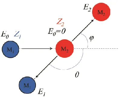
Figure 2.2. Interaction of the projectile of mass M1 and the target ion of mass M2. ... 9
Figure 2.3. The kinematic factor k as function of the scattering angle for the different target elements for H+ beam. ... 10 Figure 2.4. Schematic diagram of RBS experiment. ... 10
Figure 2.5 Schematic of of the energy loss processes in a thin layer. ... 12
Figure 2.6 Schematic RBS spectrum of Co3Pt thin film on MgO substrate (simulated in
SIMNRA program). ... 14
Figure 2.7. Schematic structures explaining the difference between (a) aligned along the <100> direction and (b) random scattering geometry for strontium titanate... 15
Figure 2.8 Schematic diagram of ion trajectories undergoing scattering at the surface and channeling within the crystal. Inset (a) shows the formation of a shadow cone behind a surface atom bombarded by ion beam... 16
Figure 2.9 Schematic of the close-encounter probability as a function of the angle between the ion beam and the symmetry direction. ... 17
Figure 2.10. Rutherford Backscattering spectra using 1.7 MeV He ions on SiC crystal implanted with 140 keV Ne ions. ... 18
Figure 2.11. Collision cascade simulated by SRIM 2008 following the penetration of a single 30 keV Fe ion in amorphous strontium titanate: red dashed line denotes the primary ion’s track; green, blue and pink lines represent trajectories of Sr, Ti and O recoil atoms, respectively. . 22
Figure 2.12. Schematic diagram of Tandetron facility. ... 24
Figure 2.13 General interaction of photon with a solid. ... 26
xii Figure 2.15. Survey XPS spectrum of strontium titanate surface cleaned by Ar sputtering.
It shows peaks from Sr, Ti and O, as well as peaks from Cu, Si and Ar impurities. ... 28
Figure 2.16. Electronic transitions caused by the absorption of X-ray photon absorption: left panel illustrates the creation of the core hole due to excitation of an electron, right panel shows radiative transitions of the cascade process that generates X-ray fluorescence (hνf) and
optical photons (hνop). ... 31
Figure 2.17. XANES and EXAFS parts of X-ray Absorption Fine Structure (XAFS) spectrum. 32
Figure 2.18. Single (a) and multiple (b) scattering processes. ... 33
Figure 2.19. Interaction of the incident X-ray beam with sample of the thickness t. ... 34
Figure 2.20. Schematic diagram of (a) dc SQUID and (b) rf SQUID. ... 36
Figure 3.1. Cubic perovskite structure of ABO3 compound: yellow, purple and blue
spheres represent A ion, B ions and oxygen ions, respectively. ... 41
Figure 3.2. Deviation from ideal cubic structure of SrTiO3 (tolerance factor t = 1) in other
perovskite compounds due to differences in radii of A and B ions: hexagonal structure
of BaNiO3 (t > 1) and Jahn-Teller distortion in LaMnO3 (t < 1). ... 41
Figure 3.3. Ti L-edge Electron Energy Loss spectra of SrTiO3: (a) EEL spectra collected at
different depth of SrTiO3 crystal; (b) the bulk and the surface contribution extracted
from the experimental spectra. ... 43
Figure 3.4. Structure of graphite: (a) ABA (Bernal stacking) and (b) ABC (Rhombohedral
stacking) arrangement. ... 45
Figure 3.5. Point defects in a graphite layer: (a) Stone-Wales defect SW(55-77), formed by rotating a carbon-carbon bond by 90°; (b) single vacancy V1(5-9); (c) Double vacancy V2
(5-8-5). ... 47
Figure 3.6. Formation energy per vacancy as a function of the nanohole size. The size is
measured as the number n of vacancies that constitute the nanoholes. ... 48
Figure 3.7. Atomic configurations of adatoms on the graphite surface. Carbon adatoms: (a) single carbon adatom in the bridge configuration; (b) single carbon adatom in the dumbbell
configuration; (c) typical configuration of metal adatom adsorbed on single vacancy; and (c) typical configuration of metal adatom adsorbed on double vacancy. Side view shows that all the configurations are non-flat. The small dark circles denote carbon atoms; big (blue) lighter circles correspond to metal atoms. ... 49
Figure. 3.8. Irradiation of graphene sheet with N and B ions: probabilities for different defect
xiii Figure 3.9. Nitrogen and oxygen groups on the surface of graphite.. ... 51
Figure 4.1 Strontium titanate band structure calculated for 40 atom supercell for pure STO and STO with oxygen vacancies. ... 58
Figure 4.2. (a) Schematics of Fe ion implantation in strontium titanate crystal. (b) SRIM simulation of distribution of Fe ion and oxygen vacancies produced during implantation as function of depth. ... 61
Figure 4.3. (a) PIXE spectra of un-implanted STO crystal and Fe implanted sample STO-Fe2e16. (b) Magnified portion with Fe Kα and Mn Kα peaks ... 62
Figure 4.4. (a) PIXE spectra of Fe implanted sample STO-Fe2e16 and implanted and annealed samples STO-Fe2e16-300C and STO-Fe2e16-350C. (b) Magnified portion with Fe Kα and
Mn Kα peaks. ... 62
Figure 4.5. (a) PIXE spectra of Fe implanted sample STO-Fe2e16 and implanted and annealed samples STO-Fe2e16-350C. (b) Magnified portion with Fe Kα and Mn Kα peaks. ... 63
Figure 4.6. RBS spectra of virgin STO crystal and STO samples implanted with different Fe+doses (STO-Fe2e14, STO-Fe8e14, and STO-Fe2e16) collected in random
geometry. ... 66
Figure 4.7. RBS spectra collected in aligned geometry: (a) STO and (b) STO Fe2e16 with
element contributions calculated in SIMNRA program. ... 67
Figure 4.8. RBS spectra of (a) STO, STO Fe2e16 and STO Fe2e16 350 C samples; and (b) STO, STO Fe1e16 and STO Fe1e16 350 C samples collected in random geometry with 0.5 MeV He+ beams. ... 68 Figure 4.9. RBS spectra of STO, STO Fe2e16 and STO Fe2e16 350C samples collected in
channeling geometry with 0.5 MeV He+ beams. ... 69 Figure 4.10 RBS spectrum of STO Fe2e16 sample collected at random geometry
with 3.03 MeV He+ beam. ... 70 Figure 4.11. (a) Ti 2p peaks in XPS spectra of implanted STO crystal; (b) comparison of
un-implanted STO, un-implanted STO-Fe2e16 and un-implanted and annealed STO-Fe2e16-350C samples collected at the surface. ... 72
Figure 4.12. XPS 1s Sr peaks of STO crystal collected after sputtering 10 nm layer. ... 72
Figure 4.13. Sr 3d peaks in XPS spectra of (a) virgin STO crystal, (b) implanted STO-Fe2e16 and (c) implanted and annealed STO-Fe2e16-350C samples collected at the surface; (d) comparison of the three STO samples following Fe implantation and anneal... 73
xiv Figure 4.15 (a) XPS Fe 2p peaks for STO-Fe2e16 sample collected at 10 nm, 20 nm, 30 nm and
40 nm depth after sputtering. (b) Depth distribution of implanted Fe derived from the
intensities of Fe 2p XPS peaks ... 75
Figure 4.16. O 1s peaks in XPS spectra of (a) STO crystal, (b) implanted STO-Fe2e16 and (c) implanted and annealed STO-Fe2e16-350C samples collected at the surface;
(d) comparison of the three STO samples following Fe implantation and anneal. ... 77
Figure 4.17. XPS 1s O peaks of STO crystal, implanted STO-Fe2e16 and implanted and
annealed STO-Fe2e16-350C samples collected after sputtering 10nm layer. ... 78
Figure 4.18 Carbon. 1s peaks in XPS spectra of (a) STO crystal, collected at the surface; (b) comparison of STO, STO-Fe2e16 and STO-Fe2e16-350C samples following Fe
implantation and anneal. ... 79
Figure 4.19. XPS 1s C peaks of STO crystal collected at surface and after sputtering at depth 10nm, 20 nm, 30 nm and 40 nm. ... 80
Figure 5.1. Ti K-edge XANES spectra of virgin STO, STO-Fe2e16 and STO-Fe2e16-350C samples. Inset shows enlarged pre-edgefeatures. ... 89
Figure 5.2. Ti L-edge XANES spectra of virgin STO, STO-Fe2e16 and STO-Fe2e16-350C samples: (a) collected in total fluorescence yield; (b) collected in total electron yield. ... 91
Figure 5.3. Fe K-edge TEY XANES spectra of STO samples: (a) implanted sample STO-Fe2e16; (b) implanted and annealed sample STO-Fe2e16-350C. Iron foil and iron oxide Fe2O3 spectra are shown for comparison. ... 91
Figure 5.4. (a) Fe L3,2-edge XANES spectra of STO implanted with different Fe+ doses; (b) Fe
L3,2-edge XANES spectra of STO implanted with different doses and annealed, collected at
the total fluorescent yield. ... 93
Figure 5.5. Fe L-edge XANES spectra of STO-Fe2e16 and STO-Fe2e16-350C collected in total fluorescence yield and in total electron yield. ... 94
Figure 5.6. O K-edge XANES spectra collected in total fluorescence yield of: (a) STO samples implanted with different Fe+ doses, and (b) STO samples implanted and annealed in oxygen atmosphere at 350°C. ... 95
Figure 5.7. O K-edge XANES spectra of virgin STO, STO-Fe2e16 and STO-Fe2e16-350C samples: (a) collected in total fluorescence yield; (b) collected in total electron yield. ... 96
Figure 5.8. Experimental Fe K-edge XANES of STO-Fe2e16 and Fe foil and FEFF calculations for Fe foil with bcc unit cell. ... 97
Figure 5.9. Comparison of the Fe K-edge XANES of STO-Fe2e16-350C sample, iron oxides and FEFF calculation for SrTi1-xFexO3-δ clusters(a) Experimental Fe K-edge XANES of
xv Experimental Fe K-edge XANES of STO-Fe2e16-350C and FEFF calculations for several mixed oxide clusters: SrFeO3, Sr Fe O8 8 23, Sr Ti Fe O8 5 3 23 and Sr Ti Fe O8 3 5 23; (d) Enlarged pre-edge
peaks. ... 99
Figure 6.1. (a) Schematic of the implantation of 2.65 MeV N+ in HOPG through Al mask; (b) SRIM simulation demonstrates distribution of N ions and C vacancies in HOPG. ... 105
Figure 6.2. (a) RBS spectra for virgin HOPG and HOPG annealed in vacuum at 450°C collected with 3.03 MeV He+ beams; (b) Magnified oxygen peak. ... 106
Figure 6.3. (a) RBS spectra recorded with He+ beam at energy 3.03 MeV for 450, HOPG-O1e16 and HOPG-O5e15 samples; (b) Magnified oxygen peak. ... 106
Figure 6.4. (a) RBS spectrum recorded He+ beam at energy 4 MeV for N irradiated sample HOPG-N1e16; (b) Magnified peaks from N for HOPG-N1e16 and HOPG-N2e15 samples. ... 107
Figure 6.5. PIXE spectra of selected HOPG samples recorded with 2 MeV H+ ions. ... 108 Figure 6.6. (a) PIXE spectra of selected HOPG samples recorded with 1 MeV H+ ions;
(b) Enlarged image of Cr, Fe and Ni peaks for HOPG, HOPG-N5e15 and
HOPG-O5e15 samples. ... 108
Figure 6.7. C K-edge TEY spectra of un-implanted graphite samples: virgin HOPG and annealed at 450°C; C K-edge TFY spectrum of HOPG annealed at 450°C is also shown. The flattened out spectral feature in TFY results from saturation (sample is optically thick). ... 111
Figure 6.8. (a) and (b) C K-edge XANES spectra of HOPG samples implanted with different doses of N and O, respectively, collected in total electron yield; (c) Enlarged graph demonstrates adsorption features in the intermediate region between C * and *
resonances. Spectrum of un-implanted HOPG is shown for comparison. ... 112
Figure 6.9. (a) C K-edge XANES spectra of HOPG-N1e16 collected in total electron yield and total fluorescent yield. (b) Enlarged pre-edge peak in TFY spectra of HOPG
samples implanted with different doses of N and O. ... 113
Figure 6.10. C K-edge XANES spectra of (a) HOPG-N1e16 and (b) HOPG-O1e16 samples, implanted and annealed in vacuum at 50°C and 100°C. ... 114
Figure 6.11 O K-edge XANES of un-implanted samples: virgin HOPG and annealed
HOPG 450 collected in total electron yield. ... 114
Figure 6.12 O K-edge XANES of HOPG samples implanted with N and O at different doses: collected in (a) total electron yield and (b) inverted fluorescence yield. ... 115
Figure 6.13 O K-edge XANES of un-implanted HOPG, HOPG N1e16, HOPG N1e16 100C and HOPG N1e16 50C samples collected in (a) total electron yield and (b) inverted
xvi Figure 6.14. O K-edge XANES of un-implanted HOPG, HOPG O1e16, HOPG O1e16 100C and
HOPG O1e16 50C samples collected in (a) total electron yield and (b) inverted
fluorescence yield. ... 116
Figure 6.15 N K-edge XANES spectra of N-doped HOPG samples at doses of 21015 and 11016 ions/cm2. ... 117 Figure 6.16 Attenuation length of soft X-rays absorbed by C and N. ... 118
Figure 7.1. Values of Curie temperature calculated for various oxide materials
containing 5% of Mn doping and 3.5x10²⁰ holes per cm3. ... 124 Figure 7.2. 3d electron level of Fe0 ([Ar] 3d64s2): (a) “high” spin configuration,
(b) “low” spin configuration. ... 126
Figure 7.3. Dependence of magnetization, M, on an applied magnetic field, H, in ferromagnetic material. ... 127
Figure 7.4. Schematic representation of (a) magnetic semiconductor, (b) non-magnetic
semiconductor, and (c) diluted magnetic semiconductor. ... 128
Figure 7.5. Superexchange interaction between d shells via O2- ions.. ... 129 Figure 7.6 Spin-split impurity band mediate ferromagnetic state. (a) Spontaneous spin-splitting;
(b) spin-splitting due to magnetic defects or impurities; (c) population of unoccupied d band by overlap with an impurity band, which lead to spin-splitting
of the latter ... 132
Figure 7.7. Schematic of charge transfer mechanism. Electrons transfer to or from the
charge reservoir to the impurity band leading to spontaneous ferromagnetic splitting. ... 133
Figure 7.8. Inhomogeneous distribution of ferromagnetic region in a dilute oxide: a) random distribution of ferromagnetic particles; b) spinoidal decomposition;
c) interface/surface defects; d) grain boundaries. ... 134
Figure 7.9. (a) C K-edge XANES spectra of HOPG and (b) corresponding magnetic hysteresis loops at each of the four steps of C+ ion implantation: 1) 70 keV and 1×10¹⁵ ion/cm2; 2) 50 keV and 3×10¹⁴ ion/cm2; 3) 30 keV and 3×10¹⁴ ion/cm2; and 4) 15 keV
and 2×10¹⁴ ion/cm2. ... 138 Figure 7.10. Magnetic moment (M) vs. field (H) curves of STO samples before subtraction of
diamagnetic component... 139
Figure 7.11 Magnetic moment (M) vs. field (H) curves of un-implanted STO and STO-350, Fe implanted samples STO-Fe2e16 and STO- Fe2e16-350, and Si implanted STO after
xvii Figure 7.12 (a) Magnetic moment (M) vs. field (H) curves of un-implanted STO and STO
implanted different Fe doses after subtraction of diamagnetic contribution; (b) enlarged part with ferromagnetic hysteresis... 142
Figure 7.13. Remanent magnetization of STO samples. ... 143
Figure 7.14. Magnetic moment of HOPG samples: (a) before and (b) after subtraction of the diamagnetic contribution. Inserts show enlarged image of hysteresis part. ... 144
xviii
List of abbreviations
2DEG two-dimensional electron gas
amu atomic mass unit
APS Advanced Photon Source
BE binding energy
CLS Canadian Light Source
DFT density functional theory
DMS dilute magnetic semiconductor
DOS density of states
EELS electron energy loss spectroscopy
EXAFS Extended X-ray Absorption Fine Structure
HBE high binding energy
HOPG Highly oriented pyrolytic graphite
KE kinetic Energy
LOD limit-of-detection
NIST National Institute of Standards and Technology
PIXE Particle Induced X-ray Emission
RBS Rutherford Backscattering Spectrometry
RKKY Rudermann–Kittel–Kasuya–Yosida interaction
SEM Scanning Electron Microscopy
SQUID Superconducting Quantum Interference Device
SRIM The Stopping and Range of Ions in Matter
STF strontium titanium ferrate SrTi1-xFexO3
STM Scanning Transmission Microscopy
STO strontium titanate SrTiO3
TEM Transmission Electron Microscopy
xix
TFY total fluorescence yield
TM transition metal
TRIM Transport of Ions in Matter
UHV ultra-high vacuum
XAFS X-ray Absorption Fine Structure
XANES X-ray Absorption Near Edge Structure
1
Chapter 1. Materials for modern technology
1.1 Motivation
The growth of digital electronics creates a great demand for new materials for
information and communication technology, processing and storage of data, photonic
technology, energy industry and others applications [1]. Recently considerable interest
has been focused on the functional perovskite oxides owing to their rich physics and great
potentials as the next-generation electronic materials. Basic research has been boosted by
a series of discoveries of their amazing properties including superconductivity, tunneling
magnetoresistance, piezoelectric, ferromagnetic, ferroelectric, and multiferroic behaviour,
resistive switching behaviour, giant thermoelectric and photoconductivity effects, and
exceptional catalytic properties [2-5]. Novel perovskite oxide materials find versatile
applications in optical electronics, gas sensors, photocatalysts, oxide cathodes, insulating
layers in random access memory, ferroelectric thin film structures, high-TC
superconductors, and gate dielectric material [6-8].
This multitude of properties comes with a price. Only a few parameters must be
controlled to obtain reliable device performance in conventional semiconductors such as
silicon. A vast knowledge has been accumulated on the microfabrication routes that do
not degrade properties and allow a system control with complex device functionality.
Numerous studies have shown that electronic, light-emitting and magnetic properties of
perovskite oxide materials depend to the greatest extent on the doping (or impurities) and
defects in different crystal structures [9].
However, the tendency to form oxygen vacancies or to develop dopant
concentration gradients in perovskite oxides significantly hinders the device fabrication.
The improved ability to control the growth of thin films and modify properties at the
atomic scale developed in recent years have extended the possibility of creating new
materials by alternating the thin-film growth of two materials on top of each other and
repeating the sequence multiple times [10]. The structures consisting only of few
2 analogs. This opens the possibility to either enhance or introduce completely new
properties that are completely absent in the parent compounds.
Until the late 1990s, the semiconductor industry has relied on silicon, a material
which is abundant and well understood, has excellent mobility properties, and offered
inexpensive fabrication routes. Silicon can be conveniently oxidized producing a SiO2
dielectric layer with a sharp interface to be used as a transistor gate insulator. However,
with further miniaturization new materials, new device geometries and new switching
concepts are required.
Intense research activity is aimed to the search of other high-mobility
semiconductor materials and new oxide materials which can replace SiO2 as a gate
dielectric material. At thickness ~ 1.2 nm silicon dioxide ceases to be perfectly insulating,
and the tunneling-induced leakage current becomes unacceptably high. Oxides with high
dielectric constant (high-κ dielectrics) can improve the operation of electronic devices.
Besides desirable dielectric constant the material should possess good thermal stability,
thermodynamic compatibility with semiconductor and low defect density at the
dielectric/semiconductor interface. Besides silicon nitride and nitrided SiO2 the
candidates were Ta2O5, TiO2, Al2O3, ZrO2, HfSixOy, and SrTiO3 films grown by atomic
layer deposition, metal-organic chemical vapour deposition, and molecular beam epitaxy
[11]. Unfortunately many of them, including TiO2 and Ta2O5, are not suitable, as they are
not thermodynamically stable in contact with Si [12].
Contemporary interest in SrTiO3 material examined in this thesis was focused on
its multiple roles in the post-Si semiconductor technology applications. First, the
excellent electrical properties of the SrTiO3/Si structures were reported with capacitance
electrically equivalent to that of an SiO2 film less than 10 Å thick [13]. Epitaxial SrTiO3
is an excellent dielectric providing a higher uniformity and lower defect density compared
to polycrystalline metal oxide films. Second, SrTiO3 can be used as a buffer layer, as its
lattice structure permits epitaxial integration with other functional transition metal oxides,
such as SrRuO3 or LaAlO3. Finally, SrTiO3, either doped with magnetic ions or
significantly reduced, can be used for spintronic applications [14]. Computing with spins
3 implemented. This information storage is non-volatile, has less power consumption and
power dissipation issues, since the operating voltages are typically lower than 1 V [15].
Another class of materials for novel post-Si technology applications is carbon
with its various allotropes and a wide range of properties [16].
Carbon-based materials comprise a huge amount of different structures from 0D
fullerene to 2D graphene and 3D graphite, diamond and so on. Introduction of defects and
doping allows us to engineer new structures and to change electronic, mechanical and
chemical properties of carbon materials [17-19]. In recent years, there have been
numerous reports of defect-induced ferromagnetism in graphite and graphene materials
which promotes their use in spintronics [20-24].
Different carbon materials are very appealing for catalytic applications both as
support for active phases and as catalyst themselves. They are environmentally friendly
and can be a cheaper replacement of conventionally used platinum catalyst. Studies have
shown that carbon-based catalysts can be applied in different fields including
hydrocarbon conversion, chemical production, fuel cells, and solar energy. Variety of
catalytic processes includes gas phase, liquid phase, oxygen reduction, and photocatalytic
reactions [25-28]. The catalytic activity of graphite can be modified and enhanced by
oxygen and nitrogen functional groups adsorbed on the surface defects. They have a
versatile potential for use in reactions of dehydration of alcohols, nitric oxide and sulfur
dioxide oxidation [27, 29, 30]. Nitrogen doped carbon materials have been studied as a
substitution of Pt catalyst in fuel cell anodes [31-34].
In this thesis, I have summarized the results of the surface analysis studies of the
local structure and magnetic properties of SrTiO3 and highly oriented pyrolytic graphite
modified by ion beams. Ion beam implantation has been routinely used in the
semiconductor industry for doping (for example, producing n- and p-type Si), fabrication
of buried layers and imbedded nanocrystals [35]. The main advantage of this approach is
that implanted doses and produced structural modification can be easily controlled by ion
beam parameters. The effect of ion irradiation on the structure and properties of materials
was studied by several methods including Rutherford backscattering spectroscopy (RBS),
particle-induced X-ray emission (PIXE), X-ray photoelectron spectroscopy (XPS), X-ray
4 device (SQUID) analysis. We found iron and iron oxide phases corresponding to the
ferromagnetic response at room temperature. Their structures were confirmed using Real
Space Multiple Scattering calculation (FEFF9).
The thesis is organized as follows. Chapter 2 discusses the experimental methods
used for sample fabrication and their analysis, including ion implantation, RBS, PIXE,
XPS and XANES that are used extensively throughout this work. SQUID measurements
were conducted at Dalhousie University by our collaborators. Therefore, in Chapter 2 we
present the theoretical background behind these methods, as well as some essential data
interpretation caveats. The idea is to provide a reader with a substantial background in
order to understand Chapters 4-7. The basic structural properties of strontium titanate and
graphite materials, as well as their defects are described in Chapter 3. Chapters 4 and 5
present RBS, PIXE, XPS and XANES experimental results for the Fe-implanted
strontium titanate. XANES is particularly suitable to study ion-irradiated systems, which
can be highly disordered or even amorphous, since no long-range crystal order is
necessary to get this information. We found correlation between observed magnetic
behaviour, Fe phases, defect concentrations and order. For better interpretation of
XANES spectra at Fe K-edge, FEFF9 calculations were performed using the Real Space
Multiple-Scattering (RSMS) formalism which takes advantage of the close connection
between XANES and electronic structure. We also observed unusual loss of Sr from the
surface layer affected by implantation. Thermodynamic parameters of several processes
involved are discussed and quantified. Experimental RBS, PIXE and XANES data for N
and O ion implanted HOPG are summarized in Chapter 6. Surprisingly, the produced
irradiation damage was similar for both ions. Defects produced by ion irradiation increase
the surface reactivity. Reaction of defective graphite surface with ambient atmosphere led
to formation of various oxygen functional groups. The origin of magnetism in oxide and
graphite materials is further considered in Chapter 7. It was recently discovered that
ferromagnetic behaviour is possible in materials that were not considered to be
traditionally magnets before. Here, our experimental SQUID results for ion implanted
strontium titanate and graphite are further considered. Chapter 8 presents the conclusion
5
References
[1] P. Ball, Electronic materials: Oxides in electronics, Mrs Bulletin 38 (2013) 873-875. [2] J.F. Schooley, W.R. Hosler, M.L. Cohen, Superconductivity in Semiconducting SrTiO3, Physical Review Letters 12 (1964) 474-475.
[3] M. Bowen, M. Bibes, A. Barthelemy, J.P. Contour, A. Anane, Y. Lemaitre, A. Fert, Nearly total spin polarization in La2/3Sr1/3MnO3 from tunneling experiments, Appl. Phys.
Lett. 82 (2003) 233-235.
[4] J.M. Rondinelli, N.A. Spaldin, Substrate coherency driven octahedral rotations in perovskite oxide films, Phys Rev B 82 (2010) 1-4.
[5] J. Wang, J.B. Neaton, H. Zheng, V. Nagarajan, S.B. Ogale, B. Liu, D. Viehland, V. Vaithyanathan, D.G. Schlom, U.V. Waghmare, N.A. Spaldin, K.M. Rabe, M. Wuttig, R. Ramesh, Epitaxial BiFeO3 multiferroic thin film heterostructures, Science 299 (2003)
1719-1722.
[6] F. Napolitano, A.L. Soldati, J. Geck, D.G. Lamas, A. Seyquis, Electronic and structural properties of La0.4Sr0.6Ti1-yCoyO3± electrode materials for symmetric SOFC
studied by hard X-ray absorption spectroscopy, International Journal of Hydrogen Energy 38 (2013) 8965-8973.
[7] R. Moos, N. Izu, F. Rettig, S. Reiss, W. Shin, I. Matsubara, Resistive Oxygen Gas Sensors for Harsh Environments, Sensors 11 (2011) 3439-3465.
[8] H. Liu, H. Dong, X. Meng, F. Wu, First-principles study on strontium titanate for visible light photocatalysis, Chemical Physics Letters 555 (2013) 141-144.
[9] J. Mannhart, D.G. Schlom, Semiconductor physics - The value of seeing nothing, Nature 430 (2004) 620-621.
[10] G. Rijnders, D.H.A. Blank, Materials science - Build your own superlattice, Nature 433 (2005) 369-370.
[11] N. Izyumskaya, Y. Alivov, H. Morkoc, Oxides, Oxides, and More Oxides: High- Oxides, Ferroelectrics, Ferromagnetics, and Multiferroics, Critical Reviews in Solid State and Materials Sciences 34 (2009) 89-179.
[12] D.G. Schlom, J.H. Haeni, A thermodynamic approach to selecting alternative gate dielectrics, MRS Bull. 27 (2002) 198-204.
[13] K. Eisenbeiser, J.M. Finder, Z. Yu, J. Ramdani, J.A. Curless, J.A. Hallmark, R. Droopad, W.J. Ooms, L. Salem, S. Bradshaw, C.D. Overgaard, Field effect transistors with SrTiO3 gate dielectric on Si, Appl Phys Lett 76 (2000) 1324-1326.
[14] J.M.D. Coey, Ariando, W.E. Pickett, Magnetism at the edge: New phenomena at oxide interfaces, MRS Bulletin 38 (2013) 1040-1047.
[15] S.J. Pearton, W.H. Heo, M. Ivill, D.P. Norton, T. Steiner, Dilute magnetic semiconducting oxides, Semicond. Sci. Technol. 19 (2004) R59-R74.
[16] M. Terrones, A.R. Botello-Mendez, J. Campos-Delgado, F. Lopez-Urias, Y.I. Vega-Cantu, F.J. Rodriguez-Macias, A.L. Elias, E. Munoz-Sandoval, A.G. Cano-Marquez, J.-C. Charlier, H. Terrones, Graphene and graphite nanoribbons: Morphology, properties, synthesis, defects and applications, Nano Today 5 (2010) 351-372.
6 [18] A.V. Krasheninnikov, F. Banhart, Engineering of nanostructured carbon materials with electron or ion beams, Nat. Mater. 6 (2007) 723-733.
[19] D.W. Boukhvalov, M.I. Katsnelson, Chemical Functionalization of Graphene with Defects, Nano Lett. 8 (2008) 4373-4379.
[20] H. Ohldag, P. Esquinazi, E. Arenholz, D. Spemann, M. Rothermel, A. Setzer, T. Butz, The role of hydrogen in room-temperature ferromagnetism at graphite surfaces, New Journal of Physics 12 (2010) 123012.
[21] M. Sepioni, R.R. Nair, S. Rablen, J. Narayanan, F. Tuna, R. Winpenny, A.K. Geim, I.V. Grigorieva, Limits on intrinsic magnetism in graphen, Physical Review Letters 105 (2010) 207205.
[22] O.V. Yazyev, Emergence of magnetism in graphene materials and nanostructures, Reports on Progress in Physics 73 (2010) 056501.
[23] R. Hohne, P. Esquinazi, V. Heera, H. Weishart, A. Setzer, D. Spemann, The influence of iron, fluorine and boron implantation on the magnetic properties of graphite, J Magn Magn Mater 320 (2008) 966-977.
[24] Z.T. He, X.M. Yang, H.H. Xia, T.Z. Regier, D.K. Chevrier, X.T. Zhou, T.K. Sham, Role of defect electronic states in the ferromagnetism in graphite, Phys Rev B 85 (2012) 144406.
[25] X.Y. Sun, R. Wang, D.S. Su, Research progress in metal-free carbon-based catalysts, Chin. J. Catal. 34 (2013) 508-523.
[26] D. Chen, A. Holmen, Z.J. Sui, X.G. Zhou, Carbon mediated catalysis: A review on oxidative dehydrogenation, Chin. J. Catal. 35 (2014) 824-841.
[27] J.L. Figueiredo, M.F.R. Pereira, The role of surface chemistry in catalysis with carbons, Catal. Today 150 (2010) 2-7.
[28] R.A. Sidik, A.B. Anderson, N.P. Subramanian, S.P. Kumaraguru, B.N. Popov, O2
reduction on graphite and nitrogen-doped graphite: Experiment and theory, J. Phys. Chem. B 110 (2006) 1787-1793.
[29] S. Biniak, G. Szymanski, J. Siedlewski, A. Swiatkowski, The characterization of activated carbons with oxygen and nitrogen surface groups, Carbon 35 (1997) 1799-1810. [30] E. Raymundo-Pinero, D. Cazorla-Amoros, A. Linares-Solano, The role of different nitrogen functional groups on the removal of SO2 from flue gases by N-doped activated
carbon powders and fibres, Carbon 41 (2003) 1925-1932.
[31] P.O. Lehtinen, A.S. Foster, Y.C. Ma, A.V. Krasheninnikov, R.M. Nieminen, Irradiation-induced magnetism in graphite: A density functional study, Physical Review Letters 93 (2004) 187202.
[32] B. Wang, Recent development of non-platinum catalysts for oxygen reduction reaction, J. Power Sources 152 (2005) 1-15.
[33] Y. Okamoto, First-principles molecular dynamics simulation of O2 reduction on
nitrogen-doped carbon, Applied Surface Science 256 (2009) 335-341.
[34] W.Y. Wong, W.R.W. Daud, A.B. Mohamad, A.A.H. Kadhum, K.S. Loh, E.H. Majlan, Recent progress in nitrogen-doped carbon and its composites as electrocatalysts for fuel cell applications, International Journal of Hydrogen Energy 38 (2013) 9370-9386. [35] J. Leveneur, G.I.N. Waterhouse, J. Kennedy, J.B. Metson, D.R.G. Mitchell, Nucleation and Growth of Fe Nanoparticles in SiO2: A TEM, XPS, and Fe L-Edge
7
Chapter 2. Experimental methods
2.1 Incident ion techniques
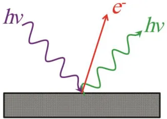
2.1.1 Ion-solid interactions
Modern techniques of material analysis are based on the interaction of particles,
including electrons, ions, and photons with matter. Ion beams are widely used for the
analysis and modification of materials. When an energetic ion collides with a solid, it can
either be elastically and inelastically scattered or it can penetrate into the solid. At
moderate energies (particles with velocity v << c), the interactions of the projectile with
the target atoms include several processes: (i) excitation or ionization of target atoms
accompanied by emission of electron and photon, (ii) transfer of energy to center-of-mass
motion of the interacting projectile and the target atom, and (iii) changes in the internal
state of the projectile. As the projectile is moving inside the target and transferring its
energy to the target atoms, it gradually slows down until it finally stops. The penetration
depth is determined by the initial kinetic energy of the projectile and the interactions with
the target atoms. Ion-solid interactions can be accompanied by emission of electron and
photon, heating of the target, formation of defects (vacancies and interstitials), and
sputtering of the target atoms.
Several ion beam analytical methods, such as Rutherford Backscattering (RBS),
and Particle Induced X-ray emission (PIXE) (Fig. 2.1) were utilized in this thesis. Ion
beams were also used for doping and material modification, as well as sputtering of the
8
Figure 2.1. Schematic processes involved in ion-solid interactions and associated techniques: Rutherford backscattering (RBS); elastic recoil detection analysis (ERDA); particle induced X-ray emission (PIXE); particle induced γ-ray emission (PIGE); secondary ions mass spectroscopy (SIMS).
Ion-nucleus interactions are dominated by the Coulomb repulsion between two
positive charges. Upon collision, ions change their energy and direction. Considering the
target ion to be at rest before collision (Fig. 2.2), simple kinematic calculations give an
expression for the energy of the projectile before scattering, E0, and after scattering, E1
and for the scattering angle [1]:
E kE M M M
M M E
1 0
1 2
2 1
2 2 1/ 2
1 2 2 0
cos sin
, (2.1)
cos ( / )(( ) / )
( ) /
1 1 2
1
2 1 1 0
0 1 0
M M E E E
E E E
o
. (2.2)
where M1 and M2 are the masses of the projectiles and target atoms, respectively. The
ratio of the energy of the scattered ions to their initial energy k E1/E0 is called the
kinematic factor.
These equations hold as long as the forces are acting along the line connecting the
9 the projectile energy exceeds the binding energy of the target atom inside solid material,
and nuclear reactions and resonances are absent.
Figure 2.2. Interaction of the projectile of mass M1 and the target ion of mass M2.
2.1.2 Rutherford Backscattering
Rutherford Backscattering spectrometry (RBS) provides information about the
elemental composition of the target as a function of depth in the near surface area (on the
order of several microns) [2]. RBS uses a monoenergetic and collimated ion beam.
Typically, He ion or proton energies are in the range of 0.5–4 MeV. The principle of RBS
analysis is described by the equation (2.1). If the mass and the initial ion energy are
known, the mass of the target ion can be easily derived by measuring the energy of
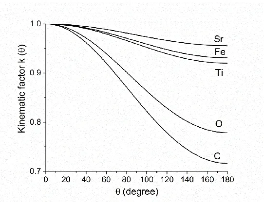
backscattered ions at any particular scattering angle. The kinematic factors, k, calculated
for the proton interaction with different elements are shown in Figure 2.3 as a function of
the scattering angle. As a general trend, the change of the proton energy after the
scattering is greater for larger scattering angles. In RBS experiments the energy of
backscattered protons are usually monitored at scattering angles close to 180º, which
provides better mass resolution (Fig. 2.4). Better mass resolution is also a reason why He
10
Figure 2.3. The kinematic factor k as function of the scattering angle for the different target elements for H+ beam.
Figure 2.4. Schematic diagram of RBS experiment.
The probability of the incident ions of energy E to be scattered into the scattering
angle θ is determined by a scattering cross-section. Differential scattering cross-section
for scattering of the incident ion of energy E by target particles is defined as
d E
d N x Q
dQ E
( , ) ( )
( )
1 1
11 where N is the volume density of atoms in the target, xis the target thickness, Q is the
total number of incident ions and dQ is the number of particles scattered into the solid
angle dΩ. Rutherford cross-section values are calculated in the assumption that the
interaction between the incident and the target ions is due to the Coulomb forces:
( ) sin/ sin cos
/ sin Z Z e
E M M M M 1 2 2 2 4 1 2 2 2 1 2 2 4 4 1 1
, (2.4)
Equation (2.4) shows that the cross section is proportional to the atomic numbers
Z1 and Z2 squared, and increases for heavier incident ions and target elements. As a
result, RBS is more sensitive to heavy elements, and the back scattering yield is higher
for heavier projectile. The cross section is higher for smaller scattering angles, and
rapidly decreases with the projectile energy (as 1 2 /E ).
Some deviations from the Rutherford values become noticeable at high and low
energies for all projectile-target pairs. For low energy projectiles (E40keV/amu) or small scattering angles, the incident particle does not completely penetrate through the
screening electron cloud.
This screening effect can be treated in the first order approximation using a
correction factor. The screened cross section is defined as:
sc ( )F, (2.5)
where the correction factorF (1 0 049. Z Z1 24 3/ /E)and the projectile energy E are
given in keV. Depending on the ion-target combination and ion energy, the screening
term lies typically in the range 085. F1 [3]. For 1MeV helium ions incident on strontium the correction factor is less than 2 %, and can be neglected for the most cases
[4]. At high energies the deviation from the Rutherford scattering cross sections is due to
nuclear interactions. The energy, at which the nuclear interactions start causing deviations
from the Rutherford cross sections, can be estimated by the equation:
E Z Z e
R
1 2 2
12 where e is elementary charge (e2
14.4 eV Å ), and R is the nuclear radius, which can beexpressed as
R
R A
o1/3
, where A is the mass number, and
R
o
14 10
.
5Å [4]. Forhelium ions incident on Si, the energy at which one should expect the deviation from the
Rutherford cross sections is ~9.6 MeV.
In some cases non-Rutherford cross sections experimentally are recorded at lower
energies (in the 2–5MeV range) and the enhancement of cross sections at these energies
help us to improve detection of light elements. For instance, for helium ions 4 He
incident on 16O, the cross section has a sharp resonance at 3.03 MeV, and it can be used to increase RBS sensitivity for oxygen detection by a factor of 15 [5]. At present, no
practical method exists for rapid accurate calculations of these non-Rutherford cross
sections; they must be measured.
2.1.3 Depth resolution
In the RBS method, only a small fraction (typically less than 0.1%) of the incident
ions get scattered from the surface layer. The majority of the ions will penetrate into the
material to depths up to several microns [6]. As the ion passes through the target, it loses
its energy on its way in and out due to interaction with the target ions and electrons. This
means that an ion scattered from the layer below the surface arrives at the detector with a
lower energy than an ion scattered from the surface as illustrated in Figure 2.5.
13 The interaction between the projectile and the targets can be described in terms of
the stopping cross section (or stopping power). The total stopping power is determined by
ion interactions with electrons and nuclei of the target atoms:
dE dx dE dx dE dx N e n e n
( ), (2.7)
where e and n are the electronic and nuclear stopping cross-sections, respectively. The
former is most important, because at typical RBS beam energies of 0.5–4 MeV the
projectile energy losses are determined mainly by the interactions with electrons due to a
higher probability of the ion-electron collisions.
The energy loss of the ions traversing through a mono-elemental target of
thickness x can be described by the equation:
E x( ) E0 N
xdx0 (2.8)
where ε is the stopping cross section.
On the other hand, it is possible to estimate the thickness of the layer if the initial
and the final energy are known:
x
N E x dE E
1
0 1 ( ) (2.9)
In a target composed of several elements the stopping power is calculated based
on the superposition of the individual stopping energy losses according to Bragg’s rule of
stopping power additivity:
cii , (2.10)
where ci and i are the concentration and the stopping power of the i th
element [7]. The
rule is accurate for metals but not for light element compounds such as organic materials,
oxides, and nitrides where the chemical and physical environments of the elements
become important [6].
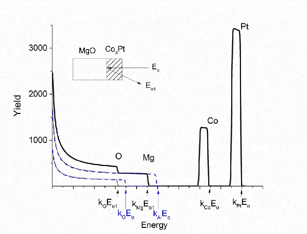
A schematic RBS spectrum of a Co3Pt thin film on MgO substrate simulated using
14 Figure 2.6. The spectrum is a superposition of the signals from the individual target
element contributions. Heavy atoms on the surface are detected at the higher scattering
energies. Backscattered ions reach the detector with the energy Ei k Ei 0, if they scatter
from the film surface. The spread in energy of Co and Pt peaks ΔE0 reflects the film
thickness. Note that the substrate surface signal appears at the energyE01 E0 E0.The
incident ions have lost part of the energy in the Co3Pt overlayer and arrived to the
substrate surface at energy E01. E0 is the energy loss in Co3Pt film. As the ions go
deeper into material and lose their energy, the scattering cross section and consequently
the ion yield increase producing the characteristic trapezoidal shape of the RBS signal.
Figure 2.6 Schematic RBS spectrum of Co3Pt thin film on MgO substrate (simulated in SIMNRA
program).
RBS is a quick, easy and relatively nondestructive method, providing information
about depth distribution of the elements. Interpretation of RBS spectra is facilitated by
computer simulation using SIMNRA program [8]. However, some previous knowledge of
the specimen composition is required to compose the target. The standard sample with
well-known composition and distribution of elements is used to convert channel number
of detector into energy. Typically, RBS provides depth resolution of 20 nm and mass
15
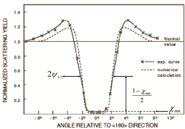
2.1.4. Channeling RBS experiments
Additional structural information can be obtained in RBS experiments by aligning
the incident ion beam with so-called channeling directions which are major symmetry
directions of the crystalline material. The probability of scattering events at such
channeling directions is greatly reduced. Figure 2.7 shows cubic perovskite structure of
strontium titanate at different geometries. If it is aligned along the <100> scattering
direction, the crystal is consists of closely packed atomic rows (Fig. 2.7(a)).
Figure 2.7. Schematic structures explaining the difference between (a) aligned along the <100> direction and (b) random scattering geometry for strontium titanate.
If the ion beam is carefully aligned with a high-symmetry direction of a crystal,
the ions are gently steered by the potential field in “channels” formed by the atomic rows.
The thermal vibration causes the atoms in the closely packed rows to deviate from their
equilibrium positions [4]. When the ion moves along the row it senses its “roughness”. As
a result it cannot approach the atomic row closer than the minimum distance rmin for
which the continuum model is valid. The interactions of a steered ion with an atomic row
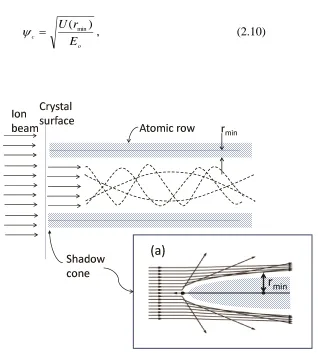
can be described by the continuum potential U r( min) that is uniformly averaged along the
row. The channeled ions move by such trajectories that they make glancing angle impact
with the atomic row at distances greater than 0.1 Ǻ from the atomic cores (Fig. 2.8) [4].
16 atomic row depends on the single continuum potential U r( min) of the row and the ion
beam energyEo:
c
o
U r E ( min)
, (2.10)
Figure 2.8 Schematic diagram of ion trajectories undergoing scattering at the surface and channeling within the crystal. Inset (a) shows the formation of a shadow cone behind a surface atom bombarded by ion beam. Adopted from Ref. [4].
The yield of channeling RBS is significantly lower compared to the yield of RBS
experiment with “random” geometry when the ion beam does not align with the
symmetry directions of the crystal (Fig. 2.7(b)). The minimum yield gives a measure of
the fraction of particles that are not channeled, i.e. the fraction of scattered ions per
number of incoming ions. In the channeling experiment for a well aligned ion beam,
critical angle 0 and the minimum distance of approach to the atomic row rmin ,
17
min( )
3
2Nd
, (2.11)where the distances d and are in Å, and the atomic concentration N is in atoms per Å2. As can be seen, the value of min is independent of the scattering parameters (Z1,
Z2 and Eo of the ion beam). It is determined only by the crystal structure. For ideal Si
crystal the minimal yield is about 3 10 2
ions per incident ion (or ~3%) [10]. In practice,
the number of visible atoms per row can be larger due to lattice imperfections and thermal
motions of the atoms.
Ions emerging from the crystal move within the same “tunnels” or channels.
Similarly, they undergo the correlated scattering and emerge from the crystal with unique
angular distribution. The phenomenon can be explained in terms of blocking. Figure 2.9
shows the close-encounter probability as a function of the scattering angle between the
ion beam and the high-symmetry direction. If ions emerge at angles, which are slightly
bigger than the critical angle, they have probability to be scattered slightly higher than 1.
18 Channeling RBS is a convenient method to study radiation-induced disorder in
crystals. During ion implantation experiments, doping atoms are introduced, and atoms of
the host crystal are knocked out of their places producing vacancies and interstitials.
These displaced atoms (as well as implanted impurities) block the channels inside crystal
structure, and RBS yields from the disordered part increase. By increased scattering yield,
it is possible to estimate what fraction of crystal has become disordered in the result of
ion implantation. The energy spread of the RBS yield shows how deep these
imperfections are.
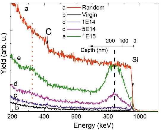
An example of RBS-channeling experiment for silicon carbide implanted with 140
keV Ne ions at different doses is shown in Figure 2.10 [11]. Yield of channeled RBS
spectrum of virgin SiC crystal is much lower than yield of the RBS spectrum collected in
random geometry. Ne irradiation produces disordered area with maximal damage located
below the surface of the crystal (at ~150 nm). Absence of Ne peak on the random RBS
spectrum shows that Ne does not incorporate into the crystal structure. With increase of
implantation dose disordering of the crystal structure increases, and de-channeling effect
becomes more obvious. Surface peak is clearly detected in the channeled RBS spectrum.
The peak appears due to interaction of incident ions with the first several monolayers of
the target crystalline structure.
19 For the experimental conditions where a laterally uniform beam of ions collides
with homogeneous target much larger than the beam size, the total number of particles A
registered by a detector can be written as follows:
A = QN x (2.12)
If and are known, and the numbers of incident (Q) and detected particles (A) are
counted, then the number of target atoms per unit area, N x [atoms/cm2], can be calculated from Equation 2.12. In practice, a common procedure for the determination of
N x is to calibrate the product Q with respect to backscattering signal from a
standard sample, e.g. Si, in which an accurately known number (N x) of heavy atoms,
e.g. Bi or Sb, is implanted per unit area.
2.1.5 Ion beam implantation
Ion beam implantation is a fabrication technique which allows us to introduce
dopants into the near-surface area in a well-controlled way. Virtually any element of the
periodic table can be implanted into almost any solid material. An ion loses its energy in
the interactions with the target until it finally stops inside the material, depending on its
energy and the density of the target. The energy and the charge of the incident ions as
well as the ion mass and the density and crystallinity of the target determine how deep it
can penetrate into the target. The doping dose is easily controlled by the ion beam current
and time. Ion dose is denoted by the total number of ions per unit area (ion/ cm2) of a target material. For high implantation dose it is possible to exceed the solubility limit of
an element in the host material which makes a promising way to fabricate
nanomaterials [12].
Energies of the ion beams vary widely in the range from 10keV to several MeV
though they can be lower or higher if different accelerators or implanters are used. At low
energies, the implanted ions are distributed near the surface, for instance Au+ implanted in alumina at the incident energy of 10 keV have an ion range of 8 nm from the surface.
At higher energy, ions can penetrate deeper into material forming buried layers.
20 lighter ion penetrates deeper into material than a heavier one. For instance, H+ ions with the incident energy of 10 keV have an ion range of 90 nm in alumina.
When energetic ions hit a target, they lose their energy in the interactions with the
electrons and the nuclei of the target. In the induced collision cascade, a high number of
vacancies and interstitials are produced (Fig 2.11). Part of the target atoms can be ejected
from the surface as recoiled or sputtered particles. The sputtering process prevails at low
incident energy (0.5–20 keV), grazing incident angles and heavier incident ions.
Typically, interstitials lie deeper in the target than vacancies. Being mobile they are able
to form vacancy clusters (or voids), interstitial clusters, interstitial and
dopant-vacancy clusters [10].
Irradiation damage depends on the type of the incident ions, on the energy,
fluence and flux of the incident ions, as well as the target material which determine
damage evolution, amorphization, dynamic defect recovery, and dynamic
recrystallization processes [13-16].
The damage increases with the increase of the ion fluence (or implantation dose).
At high dose amorphization of the surface layer occurs. Meldrum et al. [13] have studied
the amorphization of several perovskite crystals (CaTiO3, SrTiO3, BaTiO3, LiNbO3,
KNbO3, LiTaO3, and KTaO3) resulting from the bombardment with 800 keV Kr+, Xe+,
and Ne+. They found that the oxide surfaces could not be amorphized by light Ne+ ions but they were readily amorphized by Kr+ and Xe+.
The current or the flux of the ion beam, i.e. the rate at which ions arrive to the
target surface per the unit time, is an important implantation parameter for the
implantation process. Because ion bombardment causes an increase of the local
temperature of the target, the self-annealing process is often competing with the
irradiation damage. At low rate (or low beam current), the system has time to partially
recover from the irradiation damage. At fast arrival rate (or high beam current), the ion
beam can cause an accumulation of damages and, at the same time, a significant rise of
target temperature, which increases the diffusion rate of atoms and the recombination rate
of defects in the target material (vacancies and interstitials).
The critical temperature Tc above which the material cannot be amorphized is