Low Power Test Pattern Generation
Rashmitha1, Niju Rajan2
PG Student, Department of ECE, NMAMIT, Nitte, Karnataka, India1
Assistant Professor, Department of ECE, NMAMIT, Nitte, Karnataka, India2
ABSTRACT: Modern Integrated Circuits consist of more transistor count in single chip. Testing of such chip is challenging and consumes more power than functionality of the circuits. Power consumption of any VLSI circuit indicates the lifetime of the device. Therefore reducing the power consumption of VLSI design is crucial topic. The test patterns are generated by Standard LFSR, which has high switching activity within the circuit there by more power consumption. By using technology called Low power LFSR, switching activity can be reduced by inserting the three intermediate vectors between two successive test patterns.
KEYWORDS: VLSI, Switching activity, Standard LFSR, Low power LFSR
I. INTRODUCTION
Very Large Scale Integration (VLSI) Design flow mainly consists of specification, implementation, and manufacturing as its three main steps as shown in Figure 1 [1]. Functionality of the VLSI circuit is described by specifications and it is done with the help of Hardware Description Languages at various levels of abstraction. Implementation can be either full custom or semicustom. The final step of the VLSI design flow is manufacturing and is the dominant technology for VLSI circuits. Testing of the design plays an important role in the VLSI design flow and it consumes more power compared to the normal or function mode. In Complementary Metal Oxide Semiconductor (CMOS) circuits, power dissipation is proportional to the switching activity. Reducing the number of transitions in the circuit, reduces the power dissipation [2]. Low power LFSR which generates pseudo random test patterns increases the correlation between the patterns by reducing the switching activities.
Figure 1: VLSI design flow [1]
Testing of the system is done to avoid the defective component in the system rather than replacing the component later [3]. Once circuit is designed, it is important to test the circuit for their proper function and usability. Cost of the testing is one of the important factor in testing and it is depending on the testing time and circuit complexity. Good Test Pattern Generator (TPG) consumes large time and higher test data. Components within the Integrated Circuits (IC) are increased for the need of the user, so testing of the component requires powerful testing methods to check the proper function and usability of the components.
Main factors in the VLSI design are cost, reliability, performance, area and power. Power dissipation is one of the main problem during testing of the VLSI circuits. This power dissipation causes problems in today’s communication systems and portable computing devices. Static and dynamic power dissipation has major issues for the power consumption during test. Leakage current is contributed from static power dissipation and the total leakage current for power
Specification
Verification
Implementation
Manufacturing
dissipation is very small during testing mode of VLSI circuits. Dynamic power dissipation of any VLSI circuit is more compare to static power and it is due to the switching activity within the test patterns. Reduction of the dynamic power in the circuit will reduce the total test power. During testing, if the switching activity between the patterns decreases, correlation will increase and hence low power dissipation.
During 1990’s Design For Testability (DFT) played an important role in the design of VLSI circuits [5]. In olden days DFT technique played a role in timing of test application, coverage of faults and quality of test and length of test patterns. But today’s Automatic Test Pattern Generator (ATPG) produces less number of test patterns that should cover most of the scenarios of the test. Power dissipations in the testing mode is greater than the normal mode [6]. There are four main reasons for test power dissipations [7] to overcome these new clock system is designed. Two types of testing [9] external testing and internal testing, external testing uses Automatic Test Equipment (ATE) which includes input pattern generator, testing circuit and decision circuit.
II. TESTPATTERNGENERATION
By avoiding the frequent transition between the primary inputs correlation can be improved hence minimum dynamic power consumption. Standard LFSR will produces test patterns with the high switching activity. Low power LFSR is a new technique of test pattern generation to reduce the switching power by inserting three intermediates between the two consecutive successive test vectors. The total number of transition between the five vectors in Low power LFSR is equal to the transition of two vectors in Standard LFSR approach.
III.STANDARDLFSRTESTPATTERNGENERATION
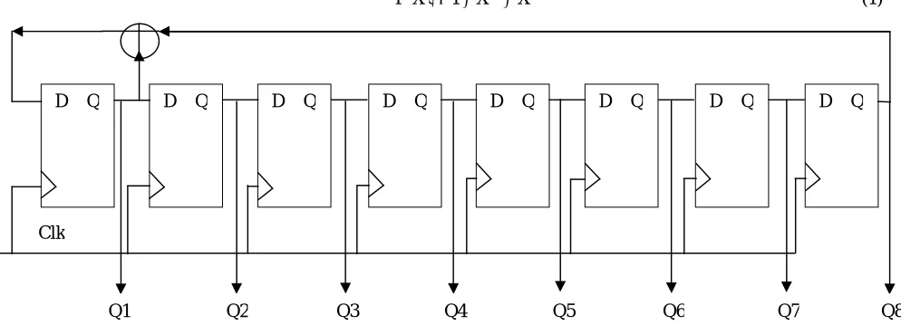
Standard LFSR is one of the pseudorandom test pattern generation. Standard LFSR consists of a series connection of flip-flops with multiplexer. The feedback is taken from certain flip-flop output taps which are XOR-ed together. Standard LFSR will produce 2 -1 test patterns, where n is the total number of bit. Logic design of 8 bit Standard LFSR is shown in Figure 2. The feedback taps are selected based on the polynomial equation, the design has taps at first and last flip-flop the design equation is as given in equation 1.
8X 1 X 1 X
P (1)
Figure 2: 8 bit Standard LFSR test pattern generation
IV.LOWPOWERLFSRTESTPATTERNGENERATION
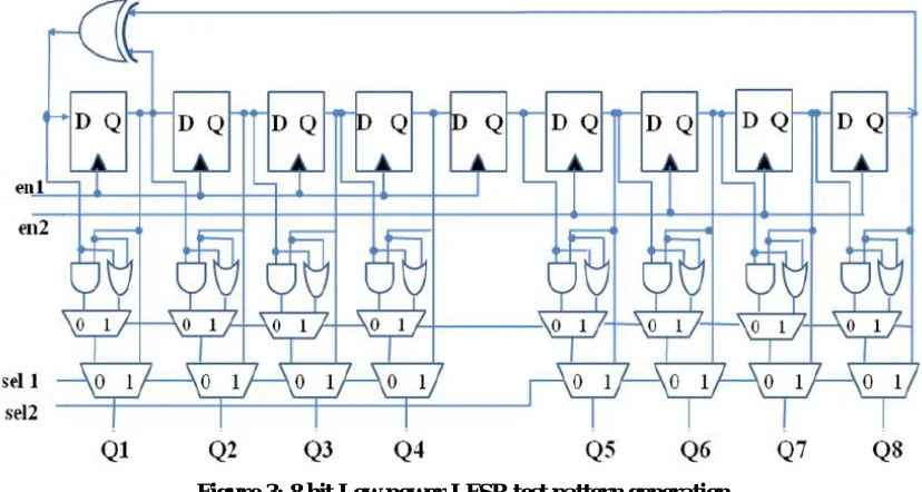
Modified Low power LFSR is designed by inserting two logic levels. The first hierarchy consists of the basic logic block such as AND and OR gates. The second hierarchy consists of multiplexer, the multiplexer output is considered as
D Q D Q D Q D Q D Q D Q D Q D Q
Clk
the output of the Low power LFSR. The design of Low power LFSR has serially connected flip-flops with AND gate, OR gate and multiplexer [1]. The output of last flip-flop is given to the input to the first flip-flop as feedback. Design equation is given in equation 1.The logic design of 8 bit Low power LFSR is shown in Figure 3.
Figure 3: 8 bit Low power LFSR test pattern generation
TECHNIQUES TO PRODUCE LOW POWER LFSR
Avoiding the frequent transition of logic level of primary inputs can increase the correlation and hence low power consumption [3]. 01001011 is considered as the seed vector of flip-flops with 9 bit LFSR. The new technique involves inserting three intermediate Ai1, Ai2 and Ai3 between Ai and Ai+1 vectors which increases the correlation between vectors and reduces the switching activity. Generation of Ai involves enabling the first four flip-flops and disabling the last four flip-flops. Shift the first four bit to one right (i.e 010). The feedback is taken from the output of XOR gate, the inputs for XOR gate is the output of last (i.e 1) and first (i.e 0) flip-flop, EXOR of 1 and 0 is 1, which is fed at the input of first flip-flop. The new first four bit is 1010. By disabling the last four bit the output is same as the last four bit seed vector (i.e 1011). 10101011 is the Ai pattern generated. Intermediate patterns Ai1 Ai2 and Ai3 are inserted between the consecutive vector Ai and Ai+1.
Generation of Ai+1 is similar as Ai, the seed vector for generating Ai+1 is 10100101 which is generated by the output of the current and output of last four bit of Ai3. Shift the first four bit of flip-flops to one bit right i.e 101, the output of fist bit of first four bit of flip-flops is obtained by doing the EXOR operation to the previous eighth bit to first bit output, which is 0 in this case. The first four bit of Ai+1 is 0101. The last four bit is 0101 which is same as Ai3, so Ai+1 propagated is 01010101.
V. SIMULATIONANDRESULTS
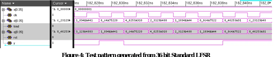
The design consists of 36 bit LFSR which has 36 stages of flops with the output taps from the first and last flip-flop. LFSR is initially fed with the test vector. Unique test patterns are generated using Standard LFSR and Low power LFSR using external clock, each clock pulse generate unique test patterns using Verilog [12]. The test pattern generated using Standard LFSR and Low power LFSR is shown in Figure 4 and 5 respectively. Equation 2 indicates the polynomial equation for 36 bit test pattern generation.
36X 1 X 1 X
P (2)
Figure 4: Test pattern generated from 36 bit Standard LFSR
Initially fed test vector generates unique patterns using external clock. The output waveform of 36 bit Standard LFSR will generate − 1 unique test patterns.
Figure 5: Test pattern generated from 36 bit Low power LFSR
Table1: Power report of test patterns
Test pattern Number of cells Leakage power consumption
(nW)
Dynamic power consumption
(nW)
Total power consumption (nW)
Standard LFSR 73 2548.386 70702.773 73251.159
Low power LFSR 131 2165.531 44991.533 47157.065
VI.CONCLUSION
The test patterns are generated using Standard LFSR and Low power LFSR with the help of Cadence NC launch Simulator. The total power consumption of Standard LFSR is 73.25 μW and it consists of 73 cells, which is obtained from Cadence RTL Compiler with 180nm technology library. The total power consumption of Low power LFSR is 47.15 μW and it has 131 cell. The power consumption of Low power LFSR is less compared to Standard LFSR even though it has more number of cells.
REFERENCES
[1] Nicola Nicolici, “Power Minimisation Techniques for Testing Low Power VLSI Circuits”, Ph.D. Thesis, University of Southampton, 2000. [2] Senthil Kumar G., Paramasivam K., “Test power minimization of VLSI circuits: survey”, 4th International Conference on Computing,
Communications and Networking Technologies (ICCCNT) 2013.
[3] Chethan J., Manjunath Lakkannavar, “Design of Low Power Test Pattern Generator using Low Transition LFSR for high Fault Coverage Analysis”, International Journal of Information Engineering and Electronic Business(IJIEEB), 2013.
[4] Hurst S. L., “VLSI Testing, Digital and Mixed Analogue/Digital Techniques”, IEEE Circuits, Devices and Systems Series 9, pp.13-15, pp.43-90, 1998.
[5] Bushnell M.L., Agrawal V.D., “Essentials of Electronic Testing”, Kluwer Academic, pp.14, 2000.
[6] Zorian Y., “A Distributed BIST Control Scheme for Complex VLSI Devices”, Proc. 11th IEEE VLSI Test Symp. (VTS 93), IEEE CS Press, pp.4-9, 1993.
[7] Girard P., Guiller L., Landrault C., Pravossoudovitch S., Wunderlich H. J.,“A modified Clock Scheme for a Low Power BIST Test Pattern Generator”, Proc. VLSI Test Symp. (VTS‟01), pp.306-311, 2001.
[8] Nourani, M., Tehranipoor, M., Ahmed, N., “Low-Transition Test Pattern Generation for BIST-Based Applications”, IEEE Transactions on Computers, pp.303-315, 2008.
[9] Abromovici M., Breuer.M.A. and Friedman, “Digital Systems Testing and Testable Design”, NJ: IEEE Press, pp.182-196, pp.457-468 and pp.477-481, 1990.
[10] Ramesh Guntupalli, “A Verilog-Based Simulation Methodology for Estimating Power and Area”, Thesis, National Institute of Technology Rourkela, 2011.
[11] web.eecs.umich.edu/~jhayes/iscas.restore/c432.html.
![Figure 1: VLSI design flow [1]](https://thumb-us.123doks.com/thumbv2/123dok_us/1518376.1186051/1.595.247.424.535.634/figure-vlsi-design-flow.webp)