Please cite this article as: G. Rajesh Kumar, K. Babulu, Low Power March Memory Test Algorithm for Static Random Access Memories,International Journal of Engineering (IJE),IJE TRANSACTIONS B: Applications Vol. 31, No. 2, (February 2018) 292-298
International Journal of Engineering
J o u r n a l H o m e p a g e : w w w . i j e . i rLow Power March Memory Test Algorithm for Static Random Access Memories
G. Rajesh Kumar*, K. Babulu
Department of Electronics and Communication Engineering, JNTUK, Kakinada, India
P A P E R I N F O
Paper history: Received 04August2016
Received in revised form 10November2017 Accepted 30November2017
Keywords:
Built in Self-test Low Power Test March Test Algorithm Memory Built in Self-test Memory Testing
A B S T R A C T
Memories are most important building blocks in many digital systems. As the integrated circuits requirements are growing, the test circuitry must grow as well. There is a need for more efficient test techniques with low power and high speed. Many memory built in self-test techniques have been proposed to test memories. Compared with combinational and sequential circuits memory testing utilizes more amount of power. Test circuitry is intensively used for memory testing. This may cause excessive power consumption during memory testing. Sophisticated and efficient techniques with less overhead on power must be needed. Regarding memories, power consumption is very much high during testing when compared with normal functional mode. March test algorithms are popular testing techniques used for memory testing. Power consumption during testing can be reduced by reducing the switching activity in test circuitry. A new test technique is proposed in this paper to reduce power consumption in test mode by reducing the switching activity in Built in Self-Test circuitry. Address sequencing in the address decoder is changed in such a way that it reduces switching activity.
doi: 10.5829/ije.2018.31.02b.13
NOMENCLATURE
↓ the address sequencing from lower address to higher address. w0 writing a byte which contains all zeroes
↑ the address sequencing from higher address to lower address w1 writing a byte which contains all ones
↕ the addresses sequencing either way r0 reading a byte from an address and checking that
retrieved information whether it is all zeroes or not.
r1 reading a byte from an address and checking that retrieved information whether it is all ones or not.
1. INTRODUCTION1
All these electronics industry achievements are sprang from Moore’s predictions. Moore predicted that the number of transistors in an integrated circuit approximately doubles in every two years. After fifty years also many inventions in electronics industry sustained Moore’s predictions. As the years are passing more and more transistors are integrated. Now millions of transistors can be integrated on a single integrated circuit. Years are passing, more and more transistors are integrated. There by circuit complexity will also
*Corresponding Author’s Email:[email protected] (G. Rajesh Kumar)
increase. In order to test such a complex circuits effective test structures are needed.
In the field of mobile communications and embedded systems, low power consumption is one of the highly needed design factors [1]. Now a day’s most of the integrated circuits are embedded with the test circuitry to test itself. These test circuitry consume lot of power. These integrated circuits with built in test capabilities are consuming more power in test mode. Compared with normal functional mode, they consume more than twice the amount of power in test mode [2]. During testing, heat is dissipated; because of high power consumption may damage the circuit [3]. While, going with low power devices, test circuitry must be of low power consuming.
System on a single chip reduces the hardware integration costs. Most of the embedded integrated circuits have memory blocks integrated inside. It is observed that the system on a chip has nearly 50% of memory related component in the architecture. In total chip area, memory components region is very much high. It is expected that, in the fourth coming years, memory portion in the total chip area may reach to 94% [4]. If the test circuitry used to test memory blocks in these integrated circuits consumes high amount of power, batteries operated devices need to be frequently charged [5]. High power consumption may leads to circuit malfunctioning. Because of high power consumption, heat dissipated also high. High temperatures may lead to integrated circuits damage.
It is hard to test memories as technology shrinks year by year. While, technology is shrinking, more and more faults appearing in memories. Traditional memory test techniques may not solve current requirements of low power test circuitry. In order to overcome all these disturbances low power memory test techniques needed. Built in self-test techniques are used to test memories. March algorithms are generally used to test static random access memories. Different March test techniques available to test memories. Each of the test technique has unique feature of testing different faults observed in memories at different level of testing. Low power technique adopted to March algorithms to build low power consuming memory built in test structures.
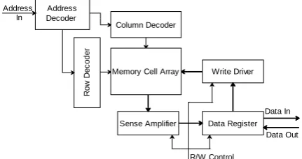
Block representation of a static random access memory (SRAM) chip is shown in Figure 1. Power
consumption in a complementary metal–oxide–
semiconductor (CMOS) logic circuit may be calculated as static power and dynamic power. Dynamic power plays an important role in testing, as the switching activity is very much high in testing mode [6]. In order to reduce power consumption during testing, the switching activity must be reduced. This can be proved by Equation (1):
T dd LV n
C
P 2
2 1
(1)
where P represents power consumption in the CMOS digital circuit. CL is the load capacitance. nT represents
the number of transitions during the time interval (0,T). It is clear that the power consumption during testing can be reduced effectively with the reduction of switching activity in testing circuits.
The rest of this paper is organized as follows. Section 2 covers the design background on memory test algorithms and low power test techniques. Section 3 describes the fault modeling. All the faults that are observed in memories are described. In section 4 March test algorithms are described. There are different March test techniques available. All are of the same kind. All these techniques are based on read and write operations
on the memory cell array in a sequential fashion. So a general structure of March algorithm is described in this section. Section 5 describes the low power March test structure. Proposed low power test technique described with clear illustrations. Simulation results of existing test technique and proposed technique are described in section 6. Comparative analysis is made with proper graphical representations.
2. MEMORY TEST BACKGROUND
Compared with normal functional mode, integrated circuits consumes more than twice power in test mode. Memory testing can be done by any one of the algorithms like zero-one algorithm, checker board algorithm, GALPAT and March test algorithms. Out of all, March test techniques are widely used due to their ease of implementation and test time. Traditional March test algorithms consumes high amount of power. In March test algorithms address decoder moving from lower address to higher address and higher address to lower address many number of times. While marching from lower address of the memory to higher address and vice versa, more number of zero to one and one to zero transitions observed in address decoder. Power consumption during memory testing can be reduced by minimizing ones and zeroes transitions in address decoder. Many researchers proposed different techniques to reduce ones and zeroes transitions in address decoder.
Different faults can be observed in static random access memory (SRAM). Out of all, 84% of the faults observed in memories are lying in five main categories [7, 8]. Stuck at faults, transition faults, coupling faults, stuck open faults and data retention faults occupy major role in memory faults. There are some other faults like Address decoder faults, neighborhood pattern sensitive faults and all occupies remaining 16%. There are many test techniques proposed to address all these faults. All those test techniques consume more amount of power due to enormous read write operations. Due to this high power consumption, devices get heated up. There by devices performance may be degraded or it may totally fail.
Figure 1. Static Random Access Memory Cell
Column Decoder
R
o
w
D
e
c
o
d
e
r
Address Decoder
Data Register Sense Amplifier
Write Driver
R/W Control
Data In
Data Out Address
In
Test time also high in traditional memory test techniques [9]. There are some methods proposed to reduce test power by reducing switching activity in test vectors [10]. By considering faults that are occurred by adjacent cells only or the faults that occur within the cells test length can be reduced [4]. Test power can be reduced by changing the order of test vectors supplied to the circuit. Test vectors are applied to the circuit in such a way that the switching activity was reduced. While supplying test vectors care must be taken to maintain test time unaltered. There are so many memory test techniques available. Many researchers proposed different memory test techniques. All of them are not optimized solutions. Zero-one technique, checker board, walking 1/0, GALPAT and sliding diagonal are some popular memory test techniques [11]. These test techniques are for finding faults observed in read write operations, memory cell array and address decoder.
3. TYPES OF FAULTS
The abstracted functional level representation of the defect is defined as a fault [12]. Different faults can be observed in memories [13-17]. These faults must be detected and diagnosed in order to improve the product quality, reliability and yield [17].
3. 1. Stuck at Faults Generally stuck at fault is because of a signal or a pin stuck at logic ‘0’ or logic ‘1’. When the signal is stuck at logic ‘0’ then it is called stuck at 0 fault. In the same way when a signal is stuck at logic ‘1’ is called stuck at 1 fault. A signal value is not changing when it supposed to be changed is a faulty behavior of the circuit. This type of faults can be observed in digital circuits. Where as in memories, a cell may stuck at logic ‘0’ or logic ‘1’. When a cell is stuck at logic ‘0’ and is not changing for any logical input pattern supplied then it is called stuck at 0 fault. In the same way when a cell is stuck at logic ‘1’ and is not changing for any logical input pattern supplied then it is called stuck at 1 fault.
Figure 2. Memory Built in Self Test Structure
3. 2. Transmission Faults When a signal or line failed to toggle from logic ‘1’ to logic ‘0’ or from logic ‘1’ to logic ‘1’ is called a transition fault. In case of memories a cell is failed to toggle. When a cell is failed to toggle from logic ‘0’ to logic ‘1’ is called as rising transition fault. When a cell is failed to toggle from logic ‘1’ to logic ‘0’ is called as falling transition fault.
3. 3. Data Retention Faults When a logic value is stored in a cell and is not changed over a particular interval of time, then the cell not able to retain its logic value is called a Data retention fault. The cell value failed to retain its previously stored value after a particular interval of time. These type of faults generally observed in static random-access memories (SRAMs).
3. 4. Coupling Faults When a cell is modified intentionally then the other cell is changing which is not supposed to change. This type of fault is called coupling fault. Generally when a cell is written with some logic value either 0 to 1 or 1 to 0 adjacent cell is effected and changes its logic value. There are different types of coupling faults observed in memories. A cell can store a logic value only when a particular cell holds a particular logic value, either 0 or 1. This type of faults are called state coupling faults. When a cell is switching its state then the adjacent cell changes its value, called idempotent coupling fault.
3. 5. Address Decoder Faults The faults which occur in address decoder are called address decoder faults. Generally four different kinds of address decoder faults observed in memories. A cell array can never be accessed with any address. Second, with an address no cell array can be accessed. Third, a cell array can be accessed with multiple addresses. Finally, multiple addresses accessing same cell array.
4. MEMORY TESTING
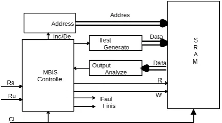
Current embedded mobile devices are developing in such a way that they are more and more user friendly. Many applications are added in single digital device. In order to accompany all these features in a single computing mobile device, the memory capacity to be incorporated also should be increased. Testing of such a huge memory is a critical task. In order to test such a high capacity memories in embedded devices high speed and low power test techniques must be used. While testing such a high capacity memory the test circuitry is intensively used. So the testing time and test power are high. Test power is very much high compared with normal functional mode power. Generally test power is several times of normal functional mode power [5]. Because of this high power device performance Address
Decoder
MBIS T Controlle
r
Test Pattern Generato
r Output Response Analyze
r Rs
t
Cl k Ru
n Faul
t Finis
h Inc/De
c
Addres s
Data In
Data Out R d W r
may degrade or the circuit logic behavior may change. To overcome all these high power effects test power must be decreased. External memory test techniques may cause excessive power consumption. Low power built in self-test techniques may be used to eliminate excessive test power. March test techniques are popularly used memory built in self-test (MBIST) architectures. General March based built in self-test structure is shown in Figure 2.
There are so many test techniques available for digital circuit testing. Out of all very few techniques developed for memory testing. All these memory test techniques are based on read and write operations on memories. March memory test MBIST architectures are widely used memory test techniques. There are so many March based algorithms available to test SRAMs. March-Y memory BIST algorithm is considered in this paper to test SRAM chips of different sizes. March-Y algorithm can be represented as:
March-Y: {↕(w0); ↑(r0,w1,r1); ↓(r1,w0,r0); ↕(r0)} This is a popular March algorithm and is able to cover all the faults that are discussed. In this representation ‘w’ indicates a write operation. ‘w0’ is for writing a byte which contains all zeroes at an address in the SRAM chip. ‘r’ indicates a read operation. ‘r0’ is for reading a byte from an address in the SRAM chip and checking that retrieved information whether it is all zeroes or not. In the same way ‘w1’ is for writing all ones and ‘r1’ is for reading a byte from memory and checking whether it is all ones or not.. The symbol ‘↕’ represents the addresses sequencing either way. Either from lower address to higher address or from higher address to lower address. The symbol ‘↑’ represents the address sequencing from higher address to lower address and the symbol ‘↓’ represents the address sequencing from lower address to higher address. Graphical illustration is shown in Figure 3.
5. LOW POWER MARCH TEST ALGORITHM
The switching activity in MBIST architectures must be reduced in order to reduce power consumption during testing. Here is a solution to reduce power consumption in memory test structures. Address decoder in MBIST structures follows binary sequence. The switching activity in binary sequencing is very much high. Consider an example where an eight bit address changing from seven to eight. While address changing from seven to eight least significant four bits are changing.
Figure 3. March Algorithm Process Flow
In the same way when the address changing from 15 to 16, least significant five bits need to be changed. So the switching activity is very much high, if the binary sequencing is used in address decoder.
March algorithms which are used to test static random access memories taking so much of time to complete test process. Because of their large computational process steps they take long time. There by power consumption also increases. In order to reduce power consumption during testing, switching activity by the test vectors must be reduced. Switching activity can be reduced by using gray code address sequences instead of using binary address sequencing [18]. Without effecting fault coverage test pattern sequence to be altered so that the switching activity can be reduced. Other researcher [18] used an algorithm to find the optimal template by updating iterations. The particles are updated with the new particles which are generated as a closer to the optimum template. All these particles are evaluated for their fitness. The particle which is giving maximum fitness function is replaced by the global best particle. This process is repeated until an optimized template is observed. Although this solution gives an optimized solution in terms of power and time, there must be a better solution with less number of iterations and less number of transitions.
Number of transitions can be reduced by changing the address sequence. Gray code address sequencing can be used to reduce switching activity [19]. Since gray code can generate a sequence with single transition, gray address sequencing will be a better solution. But the gray address sequencing logic designed is a complex one, and is not reaching the considerable change in terms of power and time. Linear feedback shift register (LFSR) based address decoder is used to generate different addresses [20]. A multiplexer is used to select the address sequencing. When the algorithm marching from lower addresses to higher address, multiplexer selects the ‘0’ input and when marching from higher address to lower address multiplexer selects ‘1’ input. Multiplexer select line decides either incrementing address or decrementing address. Figure 4 shows the logical representation of eight bit LFSR based address decoder. This address decoder lower the switching activity in memory BIST circuit. Instead of using binary sequencing in memory BIST structures, LFSR based address decoder is used. This address decoder can generate all the possible address combinations.
6. Experimental Results
Figure 4. Address Decoder with LFSR
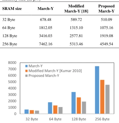
Y algorithm is used to test SRAM chips. March-Y is an 8N length memory test algorithm. Here N indicates the number of process steps, Read and Write operations. March-Y based BIST architecture is implemented. March-Y architecture uses binary address sequencing. Modified March-Y uses gray type address sequencing. Address generation can be done by using LFSR structure. LFSR structure is used to generate addresses both in incrementing order and in decrementing order. LFSR based address decoder is designed and is implemented. LFSR based address generator is able to generate both incrementing order and in decrementing order. There is a multiplexer in the address decoder, which selects whether address sequencing is incrementing or decrementing order. Exclusive OR gates are connected to the flip-flops in such a way that the LFSR is able to generate all the addresses both in incrementing order and in decrementing order. Power consumption obtained in all the cases when different size memories are tested is tabulated in Table 1. Power consumption when using Modified March algorithm also tabulated in Table 1. Also proposed March algorithm based MBIST is compared with Y MBIST and Modified March-Y [18]. Power consumption reported in Table 1 in µw units. Graphical representation of the difference is shown in Fig. 5. Graphical representation of the power report shows for different size memories when tested with March-Y algorithm. Bar chart clearly shows the power consumption difference. A considerable reduction in power consumption is observed by using proposed March structure.
March-Y algorithm is used in entire test process. Read write controller, Test controller, Address decoder and the SRAM memory array are implemented. This test circuitry can test SRAM using March-Y algorithm. This test circuitry tests SRAM by writing zeroes and ones and reading them and checking whether the retrieved information is matching with that of actually
written information or not. This writing and then reading process is not a one-time process. This type of write and read operations are performed on all the memory arrays in sequence and in multiple number of times. Here in this March-Y algorithm it is eight times. In the proposed algorithm binary sequencing is modified with low switching address sequencing generated by using LFSR. Address decoder in MBIST architecture is modified with a new address decoder constructed with LFSR. A multiplexer also used to select address sequencing either incrementing order or in decrementing order. The switching activity is reduced so the power consumption also reduced. Results obtained are tabulated and are compared with the general structure March-Y and the modified March-Y algorithm. An exponential reduction in power consumption is observed for different sized memories. This is because of the LFSR structure also becoming complex when going for higher order memories. For lower order memories the LFSR structure used is of less complex. Therefore, there is no burden of power consumption on entire test structure. While going for higher order memories the LFSR becomes complex. So the power consumption because of the LFSR structure also accounts for total test power. Even though LFSR becomes a complex structure, the total test power is less compared with any other previous test techniques. Therefore, the proposed structure is well suited for testing SRAMs.
TABLE 1. Power consumption during testing for different memory size (in µw)
SRAM size March-Y Modified
March-Y [18]
Proposed March-Y
32 Byte 678.48 589.72 510.09
64 Byte 1812.05 1315.10 1075.16
128 Byte 3416.03 2577.81 1919.08
256 Byte 7462.16 5313.46 4549.54
Figure 5. Graphical representation of power consumption during testing
0 1000 2000 3000 4000 5000 6000 7000 8000
32 Byte 64 Byte 128 Byte 256 Byte March-Y
Modified March-Y [Kumar 2010] Proposed March-Y
F F 0
F F 1
F F 2
F F 3
F F 4
F F 5
F F 6
F F 7
A 0
A 4
A 1
A 5
A 2
A 6
A 3 A7
7. CONCLUSIONS
In this paper a low power memory BIST algorithm is used to test SRAM. March-Y algorithm is used to test SRAMs. Address sequencing is altered to reduce switching activity. LFSR based address sequencing is used to reduce power consumption during testing. A new March based memory BIST architecture is implemented and is compared with traditional March algorithm and modified March algorithm. There is no change in the number of time the test process is applied on memory array, so there is no change in the fault coverage. All those faults that are discussed in this paper are covered by this algorithm. Therefore, 100 percent fault coverage can be observed with this algorithm. By considering lower size memories the LFSR structure is of less complex so a great reduction in power consumption is observed with small size memories. Whereas for large size memories the LFSR structure is a complex one. Therefore, a less reduction in power is observed due to their complex structure. Even though the LFSR becoming complex a considerable reduction in power is observed. Further high speed techniques can be applied to achieve greater speed in testing. Test time also an important factor. Therefore, low power test techniques can be combined with high speed test techniques to achieve better performance in terms of power and speed.
8. REFERENCES
1. Juneja, K., Singh, N. and Sharma, Y., "High-performance and low-power clock branch sharing pseudo-nmos level converting flip-flop", International Journal of Engineering-Transactions
C: Aspects,Vol. 26, No.3, (2012), 315-322.
2. Zorian, Y., "Testing the monster chip", IEEE Spectrum, Vol. 36, No. 7, (1999), 54-60.
3. Chandra, A. and Chakrabarty, K., "Low-power scan testing and test data compression for system-on-a-chip", IEEE Transactions on Computer-Aided Design of Integrated
Circuits and Systems, Vol. 21, No. 5, (2002), 597-604.
4. Caşcaval, P. and Caşcaval, D., "March sr3c: A test for a reduced model of all static simple three-cell coupling faults in random-access memories", Microelectronics Journal, Vol. 41, No. 4, (2010), 212-218.
5. Kumar, G.R. and Babulu, K., "A novel architecture for scan cell in low power test circuitry", Procedia Materials Science, Vol. 10, (2015), 403-408.
6. Haniba, N.B.M., Choong, F., Reaza, M.B.I., Kamala, N. and Badala, T., "Bit swapping linear feedback shift register for low power application using 130nm complementary metal oxide
semiconductor technology", International Journal of
Engineering-Transactions B: Applications, Vol. 30, No. 8
(2017), 1126-1133.
7. Kim, V.-K. and Chen, T., "On comparing functional fault coverage and defect coverage for memory testing", IEEE Transactions on Computer-Aided Design of Integrated
Circuits and Systems, Vol. 18, No. 11, (1999), 1676-1683.
8. Li, J.-F., Cheng, K.-L., Huang, C.-T. and Wu, C.-W., "March-based ram diagnosis algorithms for stuck-at and coupling faults", in Test Conference, 2001. Proceedings. International, IEEE., (2001), 758-767.
9. Gadde, P. and Niamat, M., "Fpga memory testing technique using bist", in Circuits and Systems (MWSCAS), 2013 IEEE 56th International Midwest Symposium on, IEEE., (2013), 473-476.
10. Nicolici, N. and Al-Hashimi, B., "Power-constrained testing of vlsi circuits, Springer, (2003).
11. Niamat, M., Nemade, D. and Jamali, M., "Test, diagnosis and fault simulation of embedded ram modules in sram-based fpgas", Microelectronic Engineering, Vol. 84, No. 2, (2007), 194-203.
12. Bushnell, M. and Agrawal, V., "Essentials of electronic testing for digital, memory and mixed-signal vlsi circuits, Springer Science & Business Media, Vol. 17, (2004).
13. Abadir, M.S. and Reghbati, H.K., "Functional testing of semiconductor random access memories", ACM Computing
Surveys (CSUR), Vol. 15, No. 3, (1983), 175-198.
14. Dilillo, L., Girard, P., Pravossoudovitch, S., Virazel, A. and Hage-Hassan, M.B., "Data retention fault in sram memories: Analysis and detection procedures", in VLSI Test Symposium, 2005. Proceedings. 23rd IEEE, (2005), 183-188.
15. Papachristou, C.A. and Sahgal, N.B., "An improved method for detecting functional faults in semiconductor random access memories", IEEE Transactions on Computers, Vol., No. 2, (1985), 110-116.
16. Suk, D.S. and Reddy, S.M., "A march test for functional faults in semiconductor random access memories", IEEE
Transactions on Computers, Vol. 12, No. C-30, (1981),
982-985.
17. Vardanian, V.A. and Zorian, Y., "A march-based fault location algorithm for static random access memories", in On-Line Testing Workshop, 2002. Proceedings of the Eighth IEEE International, IEEE. (2002), 256-261.
18. Kaundinya, S. and Chattopadhyay, S., "Particle swarm optimization based scheme for low power march sequence generation for memory testing", in Test Symposium (ATS), 2010 19th IEEE Asian, IEEE. (2010), 401-406.
19. Cheung, H. and Gupta, S.K., "A bist methodology for comprehensive testing of ram with reduced heat dissipation", in Test Conference, 1996. Proceedings., International, IEEE. (1996), 386-400.
20. Kim, Y.-H., Hong, I.-S., Jung, J.-M., Kim, Y.-O. and Lim, I.-C., "An efficient test procedure for functional faults in semiconductor random access memories", Journal of Circuits,
Low Power March Memory Test Algorithm for Static Random Access
Memories
TECHNICAL NOTE
G. Rajesh Kumar, K. Babulu
Department of Electronics and Communication Engineering, JNTUK, Kakinada, India
P A P E R I N F O
Paper history: Received 04August 2016
Received in revised form 10November 2017 Accepted 30November 2017
Keywords:
Built in Self-test Low Power Test March Test Algorithm Memory Built in Self-test Memory Testing
ديكچ ه
قن لاتيجید یاهمتسيس تخاس رد هظفاح ش
ه .دنیامن یم دافیا ار یمهم اهرادم هكنانچم
هظفاح ی دنا دشر لاح رد
یاه هظفاح .دشاب یم زاين دروم لااب تعرس و نيئاپ ناوت اب رثوم دتم .دیامن دشر دیاب زين رادم تست و نومزآ دوخ
-پ هظفاح تست یارب امزآ ي
.تسا هدش داهنش و یرس یاهرادم
یاهرادم فرصم یدایز ناوت هظفاح نومزآ یارب یبيکرت
یم یامن ظفاح نومزآ یارب رادم نومزآ .دن ه
.دوش یم هدافتسا یا
رما ن .تسا هدش ناوت هیور یب فرصم بجوم
نيئاپ فرصم ناوت اب هديچيپ و رثوم یاهشور اين
.تسا دنمز نومزآ ماگنه
رادم رد هظفاح یداع تلاح ناوت فرصم
ناوت یم ار یفرصم ناوت هظفاح تست یارب هک تسا یلوادتم نومزآ شور سرام نومزآ متیروگلا .تسلااب د
شهاک
داد ار رادم تست تيلاعف و یبوخب زين
د ماجنا ده رادم نومزآ یارب یفرصم ناوت هلاقم نیا رد هدش هئارا نیون شور .
شهاک ار هظفاح هداد
ضیوعت و دک بيترت هولاعب .ددرگ یم ناوت فرصم شهاک بجوم هک تسا یقیرط هب رادم