Chapter 10
What is Serial Peripheral Interface (SPI)?
•
SPI is a synchronous serial protocol proposed by Motorola to be used as
standard for interfacing peripheral chips to a microcontroller.
•
Devices are classified into the master or slaves.
•
The SPI protocol uses four wires to carry out the task of data
communication:
– MOSI: master out slave in – MISO: master in slave out – SCK: serial clock
– SS: slave select
•
An SPI data transfer is initiated by the master device. A master is
responsible for generating the SCK signal to synchronize the data transfer.
•
The SPI protocol is mainly used to interface with shift registers, LED/LCD
The HCS12 SPI Modules
• An HCS12 device may have from one to three SPI modules.
• The MC9S12DP256 has three SPI modules: SPI0, SPI1, and SPI2. • By default, the SPI0 share the use of the upper 4 Port S pins:
– PS7 SS0 (can be rerouted to PM3) – PS6 SCK0 (can be rerouted to PM5) – PS5 MOSI0 (can be rerouted to PM4) – PS4 MISO0 (can be rerouted to PM2)
• By default, the SPI1 shares the use of the lower 4 Port P pins:
– PP3 SS1 (can be rerouted to PH3) – PP2 SCK1 (can be rerouted to PH2) – PP1 MOSI1 (can be rerouted to PH1) – PP0 MISO1 (can be rerouted to PH0)
• By default, the SPI2 shares the use of the upper 4 Port P pins:
– PP6 SS2 (can be rerouted to PH7) – PP7 SCK2 (can be rerouted to PH6) – PP5 MOSI2 (can be rerouted to PH5) – PP4 MISO2 (can be rerouted to PH4)
SPI Related Registers
(1 of 6)
•
The operating parameters of each SPI module are controlled via two control
registers:
– SPIxCR1: (x = 0, 1, or 2) – SPIxCR2
•
The baud rate of SPI transfer is controlled by the SPIxBR register.
•
The operation status of the SPI operation is recorded in the SPIxSR
register.
•
The contents of the SPIxCR1, SPIxCR2, SPIxBR, and SPIxSR registers are
illustrated in Figure 10.1 to 10.4, respectively.
•
The SS pin may be disconnected from SPI by clearing the SSOE bit in the
SPIxCR1 register. After that, it can be used as a general I/O pin.
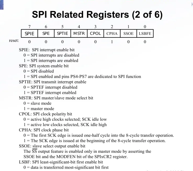
7 6 5 4 3 2 1 0
reset: 0 0 0 0 0 1 0 0
MSTR CPOL CPHA SSOE
SPIE SPE SPTIE LSBFE
Figure 10.1 SPI control register 1 (SPIxCR1, x = 0, 1, or 2) SPIE: SPI interrupt enable bit
0 = SPI interrupts are disabled 1 = SPI interrupts are enabled SPE: SPI system enable bit 0 = SPI disabled
1 = SPI enabled and pins PS4-PS7 are dedicated to SPI function SPTIE: SPI transmit interrupt enable
0 = SPTEF interrupt disabled 1 = SPTEF interrupt enabled
MSTR: SPI master/slave mode select bit 0 = slave mode
1 = master mode
CPOL: SPI clock polarity bit
0 = active high clocks selected; SCK idle low 1 = active low clocks selected, SCK idle high CPHA: SPI clock phase bit
0 = The first SCK edge is issued one-half cycle into the 8-cycle transfer operation. 1 = The SCK edge is issued at the beginning of the 8-cycle transfer operation. SSOE: slave select output enable bit
The SS output feature is enabled only in master mode by asserting the SSOE bit and the MODFEN bit of the SPIxCR2 register.
LSBF: SPI least-significant-bit first enable bit 0 = data is transferred most-significant bit first 1 = data is transferred least-significant bit first
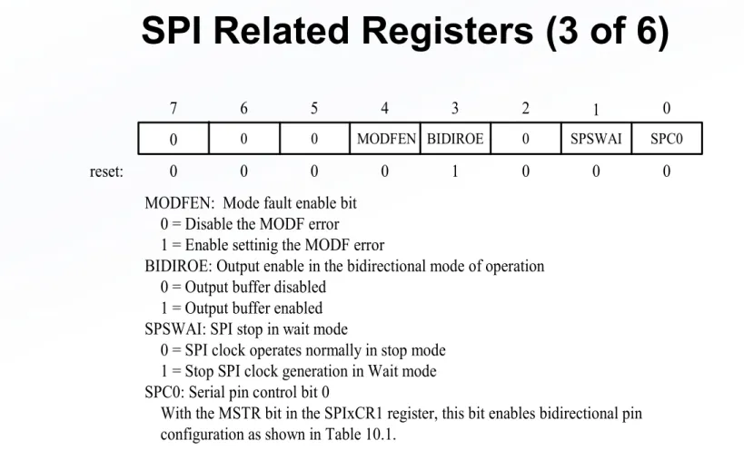
7 6 5 4 3 2 1 0
reset: 0 0 0 0 1 0 0 0
MODFEN BIDIROE 0 SPSWAI
0 0 0 SPC0
Figure 10.2 SPI control register 2 (SPIxCR2, x = 0, 1, or 2) MODFEN: Mode fault enable bit
0 = Disable the MODF error 1 = Enable settinig the MODF error
BIDIROE: Output enable in the bidirectional mode of operation 0 = Output buffer disabled
1 = Output buffer enabled SPSWAI: SPI stop in wait mode
0 = SPI clock operates normally in stop mode 1 = Stop SPI clock generation in Wait mode SPC0: Serial pin control bit 0
With the MSTR bit in the SPIxCR1 register, this bit enables bidirectional pin configuration as shown in Table 10.1.
MODFEN SSOE Master Mode Slave mode 0
0 1 1
0 1 0 1
SS not used by SPI SS not used by SPI
SS input with MODF feature SS output
SS input SS input SS input SS input Table 10.1 SS input/ output selection
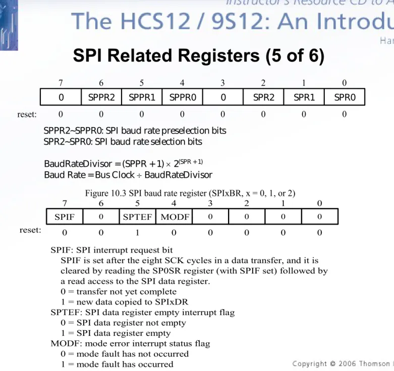
7 6 5 4 3 2 1 0
reset: 0 0 0 0 0 0 0 0
SPPR0 0 SPR2 SPR1
0 SPPR2 SPPR1 SPR0
Figure 10.3 SPI baud rate register (SPIxBR, x = 0, 1, or 2)
SPPR2~SPPR0: SPI baud rate preselection bits SPR2~SPR0: SPI baud rate selection bits
BaudRateDivisor = (SPPR + 1) 2(SPR + 1) Baud Rate = Bus Clock BaudRateDivisor
7 6 5 4 3 2 1 0
reset: 0 0 1 0 0 0 0 0 MODF 0 0 0
SPIF 0 SPTEF 0
Figure 10.4 SPI status register (SPIxSR) SPIF: SPI interrupt request bit
SPIF is set after the eight SCK cycles in a data transfer, and it is cleared by reading the SP0SR register (with SPIF set) followed by a read access to the SPI data register.
0 = transfer not yet complete 1 = new data copied to SPIxDR
SPTEF: SPI data register empty interrupt flag 0 = SPI data register not empty
1 = SPI data register empty
MODF: mode error interrupt status flag 0 = mode fault has not occurred 1 = mode fault has occurred
SPI Related Registers (6 of 6)
• Example 10.1 Give a value to be loaded to the SPIxBR
register to set the baud rate to 2 MHz for a 24 MHz bus
clock.
• Solution: 24 MHz
2 MHz = 12. One possibility is to set
SPPR2-SPPR0 and SPR2-SPR0 to 010 and 001,
respectively. The value to be loaded into the SPIxBR
register is $21.
• Example 10.2 What is the highest possible baud rate for
the SPI with 24 MHz bus clock?
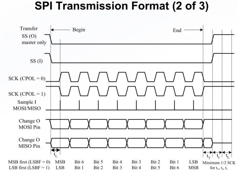
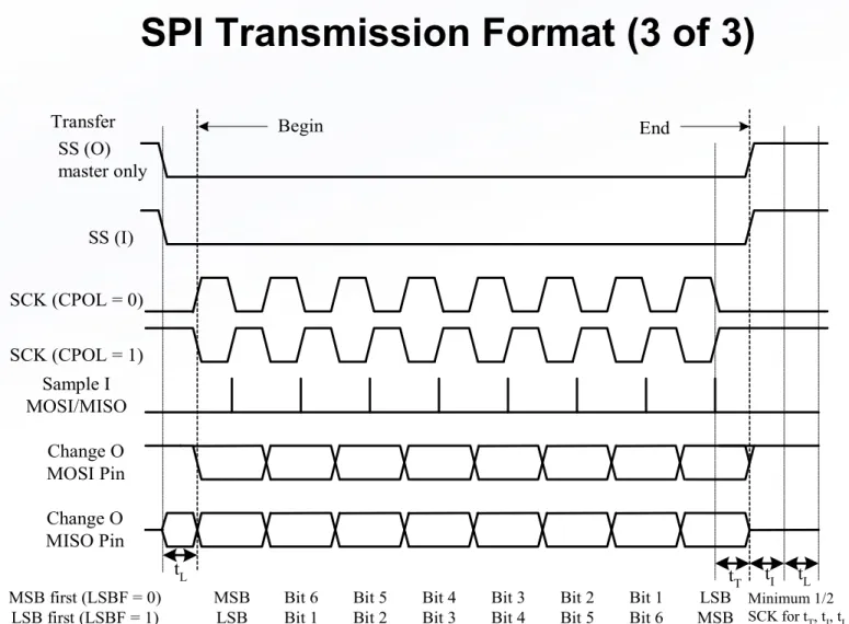
SPI Transmission Format (1 of 3)
• The data bits can be shifted on the rising or the falling
edge of the SCK clock.
• Since the SCK can be idle high or idle low, there are four
possible combinations as shown in Figure 10.5 and 10.6.
• To shift data bits on the rising edge, set CPOL-CPHA to
00 or 11.
• To shift data bits on the falling edge, set CPOL-CPHA to
01 or 10.
SS (O) master only
SS (I)
SCK (CPOL = 0) SCK (CPOL = 1)
Sample I MOSI/MISO
Change O MOSI Pin Change O MISO Pin
tT tI tL
Minimum 1/2 SCK for tT, tI, tL
tL MSB first (LSBF = 0)
LSB first (LSBF = 1)
MSB LSB
Bit 6 Bit 1
Bit 5 Bit 2
Bit 4 Bit 3
Bit 3 Bit 4
Bit 2 Bit 5
Bit 1 Bit 6
LSB MSB
Begin End
Transfer
Figure 10.5 SPI Clock format 0 (CPHA = 0)
SS (O) master only
SS (I)
SCK (CPOL = 0) SCK (CPOL = 1)
Sample I MOSI/MISO
Change O MOSI Pin Change O MISO Pin
tT tI tL
Minimum 1/2 SCK for tT, tI, tL
tL MSB first (LSBF = 0)
LSB first (LSBF = 1)
MSB LSB
Bit 6 Bit 1
Bit 5 Bit 2
Bit 4 Bit 3
Bit 3 Bit 4
Bit 2 Bit 5
Bit 1 Bit 6
LSB MSB
Begin End
Transfer
Figure 10.6 SPI Clock format 1 (CPHA = 1)
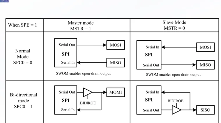
Bidirectional Mode (MOMI or SISO)
• A mode that uses only one data pin to shift data in and out.
• This mode is provided to deal with peripheral devices with only one data pin. • Either the MOSI pin or the MISO pin can be used as the bidirectional pin.
• When the SPI is configured to the master mode (MSTR bit = 1), the MOSI pin is used in data transmission and becomes the MOMI pin.
• When the SPI is configured to the slave mode (MSTR bit = 0), the MISO pin is used in data transmission and becomes the SISO pin.
• The direction of each serial pin depends on the BIDIROE bit of the SPIxCR2 register. • The pin configuration for MOSI and MISO are illustrated in Figure 10.7.
Figure 10.7 Normal mode and bidirectional mode
Serial Out
SPI
Serial In
MOSI
MISO When SPE = 1
Normal Mode SPC0 = 0
Master mode MSTR = 1
Serial Out
SPI
Serial In
MOMI
BIDIROE
Serial Out
SPI
Serial In
SISO
BIDIROE Serial Out
SPI
Serial In MOSI
MISO Slave Mode
MSTR = 0
SWOM enables open-drain output SWOM enables open-drain output
Mode Fault Error
• If the SSx signal goes low while the SPIx is configured
as a master, it indicates a system error where more than
one master may be trying to drive the MOSIx and SCKx
pins simultaneously.
• The MODF bit in the SPIxSR register will be set to 1
when mode fault condition occurs.
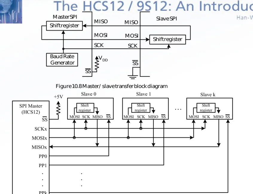
SPI Circuit Connection
• In an SPI system, one device is configured as a master.
Other devices are configured as slaves.
• The circuit connection for a single-slave system is shown
in Figure 10.8.
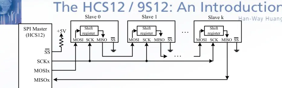
• A multi-slave system may have two different connection
methods as illustrated in Figure 10.9 and 10.10.
• In Figure 10.9, the master can exchange data with each
individual slave without affecting other slaves.
• In Figure 10.10, all the slaves are configured into a
Shift register
Shift register
Baud Rate
Generator VDD
MISO MOSI SCK SCK MOSI MISO SS SS
Master SPI Slave SPI
Figure 10.8 Master/ slave transfer block diagram
SS
+5V
MOSI SCK MISO SS Shift
register
MOSI SCK MISO SS Shift
register
MOSI SCK MISO Shift register SS SPI Master (HCS12) SCKx MOSIx MISOx PP0 PP1 PPk . . . . . . . . .
Slave 0 Slave 1 Slave k
SS
+5V
MOSI SCK MISO SS Shift
register
MOSI SCK MISO SS Shift
register
MOSI SCK MISO Shift register
SS
SPI Master (HCS12)
SCKx MOSIx MISOx
. . .
Slave 0 Slave 1 Slave k
Figure 10.10 Single-master and multiple-slave device connection (method 2)
. . .
• Example 10.3 Configure the SPI0 to operate with the following
setting assuming that E
• clock is 24 MHz:
– 6 MHz baud rate
– Enable SPI0 to master mode
– SCK0 pin idle low with data shifted on the rising edge of SCK
– Transfer data most significant bit first and disable interrupt
– Disable SS0 function
– Stop SPI in Wait mode
movb #$10,SPI0BR ; set baud rate to 6 MHz
movb #$50,SPI0CR1 ; disable interrupt, enable SPI, SCK idle low, data ; latched on rising edge, data transferred msb first movb #$02,SPI0CR2 ; disable bidirectional mode, stop SPI in wait mode movb #0,WOMS ; enable Port S pull-up
• Solution: f
E/ baud rate = 24 MHz/6 MHz = 4. We
need to set SPPR2-SPPR0 and SPR2-SPR0 to
001 and 000, respectively. Write the value $10
into the SPI0BR register.
SPI Utility Functions
• The following operations are common in many
applications and should be made into library functions to
be called by many SPI applications:
– Send a character to SPI
putcspix (x = 0, 1, or
2)
– Send a string to SPI
putsspix (x = 0, 1, or 2)
– Read a character from SPI
getcspix (x = 0, 1, or 2)
putcspi0 brclr SPI0SR,SPTEF,* ; wait until write operation is permissible staa SPI0DR ; output the character to SPI0
brclr SPI0SR,SPIF,* ; wait until the byte is shifted out ldaa SPI0DR ; clear the SPIF flag
rts
void putcspi0 (char cx) {
char temp;
while(!(SPI0SR & SPTEF)); /* wait until write is permissible */ SPI0DR = cx; /* output the byte to the SPI */
while(!(SPI0SR & SPIF)); /* wait until write operation is complete */ temp = SPI0DR; /* clear the SPIF flag */
}
; the string to be output is pointed to by X
putsspi0 ldaa 1,x+ ; get one byte to be output to SPI port beq doneps0 ; reach the end of the string?
jsr putcspi0 ; call subroutine to output the byte bra putsspi0 ; continue to output
doneps0 rts
void putsspi0(char *ptr) {
while(*ptr) { /* continue until all characters have been output */ putcspi0(*ptr);
ptr++; }
}
; This function reads a character from SPI0 and returns it in accumulator A
getcspi0 brclr SPI0SR,SPTEF,* ; wait until write operation is permissible staa SPI0DR ; trigger eight clock pulses for SPI transfer brclr SPI0SR,SPIF,* ; wait until a byte has been shifted in
ldaa SPI0DR ; return the byte in A and clear the SPIF flag rts
char getcspi0(void) {
while(!(SPI0SR & SPTEF)); /* wait until write is permissible */
SPI0DR = 0x00; /* trigger 8 SCK pulses to shift in data */ while(!(SPI0SR & SPIF)); /* wait until a byte has been shifted in */ return SPI0DR; /* return the character */
}
; This function reads a string from the SPI and store it in a buffer pointed to by X ; The number of bytes to be read in passed in accumulator B
getsspi0 tstb ; check the byte count
beq donegs0 ; return when byte count is zero jsr getcspi0 ; call subroutine to read a byte
staa 1,x+ ; save the returned byte in the buffer decb ; decrement the byte count
bra getsspi0
donegs0 clr 0,x ; terminate the string with a NULL character rts
void getsspi0(char *ptr, char count) {
while(count) { /* continue while byte count is nonzero */ *ptr++ = getcspi0(); /* get a byte and save it in buffer */
count--; }
*ptr = 0; /* terminate the string with a NULL */ }
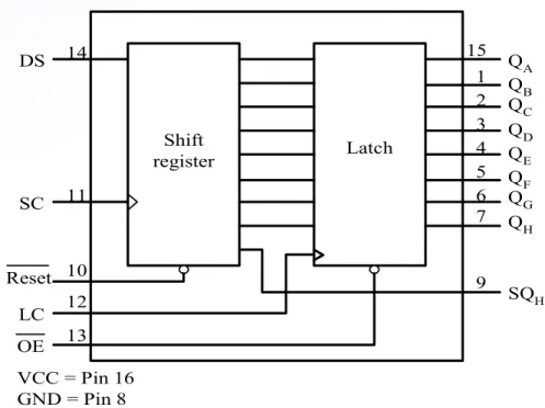
Shift register QA QB QC QD QE QF QG QH Latch SQH 15 13 1 2 3 4 5 6 7 9 12 10 11 DS 14 Reset LC OE SC
Figure 10.11 The 74HC595 block diagram and pin assignment VCC = Pin 16
GND = Pin 8
The HC595 Shift Register
• The HC595 consists of an 8-bit shift register and a D-type latch with
three-state parallel output.
Signal Pins of the HC595
• DS: serial data input
• SC: shift clock. A low-to-high transition on this pin causes the data
at the serial input pin to be shifted into the 8-bit shift register.
• Reset: A low on this pin resets the shift register portion of this
device.
• LC: latch clock. A low-to-high transition on this pin loads the
contents of the shift register into the output latch.
• OE: output enable. A low on this pin allows the data from the latches
to be presented at the outputs.
• QA to QH: tri-state latch output
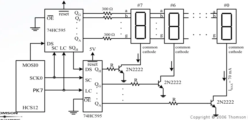
Applications of the HC595
(1 of 2)
• The HC595 is often used to add parallel ports to
the microcontroller.
a b
g
Figure 10.12 Two 74HC595s together drive eight seven-segment displays
. . . . . . . . . a b g . . . common cathode common cathode a b g
IMA
X = 7 0 m A . . . R R R 2N2222 2N2222 2N2222
300
300
#7 #6 #0
HCS12 MOSI0 SCK0 . . . SC SC DS DS SQH LC LC 5V 5V QG QF QA . . . 74HC595 74HC595 reset reset QH QG QA . . . OE OE common cathode PK7
Applications of the HC595
(2 of 2)
•
Example 10.5 Describe how to use two 74HC595s to drive eight common
cathode seven-segment displays assuming that the E clock frequency of the
HCS12 is 24 MHz.
#include “c:\miniide\hcs12.inc" org $1000
icnt ds.b 1 ; loop count
org $1500
lds #$1500 ; set up stack pointer
bset DDRK,$80 ; configure the PK7 pin for output jsr openspi0 ; configure SPI0
forever ldx #dispTab ; use X as a pointer to the table movb #8,icnt ; set loop count to 8
loop ldaa 1,x+ ; send the digit select byte to the 74HC595 jsr putcspi0 ; "
ldaa 1,x+ ; send segment pattern to 74HC595 jsr putcspi0 ; "
bclr PTK,BIT7 ; transfer data from shift register to output bset PTK,BIT7 ; latch
ldy #1 ; display the digit for one ms jsr delayby1ms ; "
dec icnt ;
bne loop ; if not reach digit 1, then next bra forever ; start from the start of the table
openspi0 movb #0,SPI0BR ; set baud rate to 12 MHz
movb #$50,SPI0CR1 ; disable interrupt, enable SPI, SCK idle low, ; latch data on rising edge, transfer data msb first movb #$02,SPI0CR2 ; disable bidirectional mode, stop SPI in wait mode movb #0,WOMS ; enable Port S pull-up
rts
#include "c:\miniide\delay.asm" #include "c:\miniide\spi0util.asm"
; ******************************************************************** ; Each digit consists of two bytes of data. The first byte is ; digit select, the second byte is the digit pattern.
; ******************************************************************** dispTab dc.b $80,$7F,$40,$70,$20,$5F,$10,$5B
#include “c:\egnu091\include\hcs12.h” #include “c:\egnu091\include\spi0util.c” #include “c:\egnu091\include\delay.c” void openspi0(void);
void main (void) {
unsigned char disp_tab[8][2] = {{0x80,0x7F},{0x40,0x70},{0x20,0x5F},{0x10,0x5B}, {0x08,0x33},{0x04,0x79},{0x02,0x6D},{0x01,0x30}}; char i;
openspi0(); /* configure the SPI0 module */ DDRK |= BIT7; /* configure pin PK7 as output */ while(1) {
for (i = 0; i < 8; i++) {
putcspi0(disp_tab[i][0]); /* send out digit select value */ putcspi0(disp_tab[i][1]); /* send out segment pattern */
PTK &= ~BIT7; /* transfer values to latches of 74HC595s */ PTK |= BIT7; /* " */
delayby1ms(1); /* display a digit for 1 ms */ }
NC CE SCK GND VDD NC SDI SDO TC72 Internal diode temperature sensor 10-bit sigma Delta A/ D converter temperature register Manufacturer ID register Control Register Serial Port Interface CE SCK SDO SDI GND
VDD TC72
Figure 10.13 TC72 pin assignment and functional block diagram 1 2 3 4 5 6 7 8
The TC72 Digital Thermometer
• 10-bit resolution and SPI interface
• Pin assignment and block diagram shown in Figure 10.13. • Capable of reading temperature from -55oC to 125oC.
• Can be used in continuous temperature conversion or one-shot conversion mode. • Has internal clock generator to control the automatic temperature conversion
Binary
high byte/ low byte
0010 0001/ 0100 0000 0100 1010/ 1000 0000 0001 1010/ 1100 0000 0000 0001/ 1000 0000 0000 0000/ 0000 0000 1111 1111/ 1000 0000 1111 0010/ 1100 0000 1110 0111/ 0000 0000 1100 1001/ 0100 0000
Hex 2140 4A80 1AC0 0180 0000 FF80 F2C0 E700 C900 Temperature
33.25oC 74.5oC 26.75oC
1.5oC 0oC -0.5oC -13.25oC
-24oC -55oC Table 10.3 TC72 Temperature output data
Temperature Data Format
• Temperature is represented by a 10-bit two’s complement word with
a resolution of 0.25oC per least significant bit.
• The converter is scaled from -128oC to +127oC with 0oC
represented as 0x0000.
• The temperature value is stored in two 8-bit registers.
Register addressRead addressWrite Bit7 Bit6 Bit5 Bit4 Bit3 Bit2 Bit1 Bit0 POR/ BORValue on Control LSB temperature MSB temperature Manufacturer ID 0x00 0x01 0x02 0x03 0x80 N/ A N/ A N/ A 0 T1 T9 0 0 T0 T8 1 0 0 T7 0 OS 0 T6 1 0 0 T5 0 0 0 T4 1 0 0 T3 0 SHDN 0 T2 0 0x05 0x00 0x00 0x54 Table 10.4 Register for TC72
Note. 1. OS is One-Shot 2. SHDN is Shutdown
TC72’s Serial Interface
• The CE input to the TC72 must be asserted (high) to enable SPI transfer.
• Data can be shifted on the rising edge or the falling edge depending on the idle polarity of the SCK source.
• Data transfer to and from the TC72 consists of one address byte followed by one or multiple data (2 to 4) bytes.
• The TC72 registers and their addresses are shown in Table 10.4.
• The most significant bit of the address byte determines whether a read (A7 = 0) or a write (A7 = 1) operation will occur.
• A multiple byte read operation will start from high address toward lower addresses. • The user can send in the temperature result high byte address and read the
Procedure for Reading Temperature
(1 of 2)
•
Step 1
– Pull the CE pin high to enable SPI transfer.
•
Step 2
– Send the temperature result high byte read address (0x02) to the TC72. Wait until the SPI transfer is complete.
•
Step 3
– Read the temperature result high byte. The user needs to write a dummy byte into the SPI data register to trigger eight clock pulses.
•
Step 4
– Read the temperature result low byte. Again, the user needs to write a dummy byte into the SPI data register to trigger eight clock pulses.
•
Step 5
– Pull CE pin to low so that a new transfer can be started.
CE
SCK
SDI
SDO High Z
A
7 A6 A5 A4 A3 A2 A1 A0
D 7 D 6 D 5 D 4 D 3 D 2 D 1 D 0
1 2 3 4 5 6 7 8 9 10 11 12 13 14 15 16
A7 = 0
Figure 10.15b Single data byte read operation
high Z CE SCK D 7 D 0 D 7 D 0 D 7 D 0 SDO Write operation Read operation A 7 A 0
Address byte = 0x02
SDI
Figure 10.15c SPI multiple data byte transfer
Operation mode
Continuous temperature conversion Shutdown
Continuous temperature conversion One-shot
One-Shot bit
0 0 1 1
0 1 0 1 Shutdown bit Table 10.5 Control register temperature conversion mode selection
Control Register
•
The control register is used to select the shutdown, continuous, or one-shot
conversion operating mode.
•
The temperature conversion mode selection logic is shown in Table 10.5.
•
At power up, the SHDN bit is 1. Thus the TC72 is in the shutdown mode.
•
If the SHDN bit is 0, the TC72 will perform a temperature conversion
approximately every 150 ms.
•
A temperature conversion will be initiated by a write operation into the
control register to select the continuous mode or one-shot mode.
CE SCK SDO SDI
PK7 SCK0 MISO0 MOSI0
HCS12 MCU TC72
VDD VDD
GND 0.1F
Figure 10.16 Circuit connection between the TC72 and the HCS12
• Example 10.6 Write a C program to read the
#include “c:\egnu091\include\hcs12.h” #include “c:\egnu091\include\spi0util.c” #include “c:\egnu091\include\delay.c” #include “c:\egnu091\include\convert.c” void read_temp (char *ptr);
void openspi0(void); char buf[10];
void main (void) {
DDRM |= BIT1; /* configure the PM1 pin for output */ openspi0(); /* configure SPI0 module */
read_temp(&buf[0]); }
void openspi0(void) {
SPI0BR = 0x10; /* set baud rate to 6 MHz */
SPI0CR1 = 0x50; /* enable SPI0 to master mode, select rising edge to shift data in and out */
SPI0CR2 = 0x02; /* select normal mode and stop SPI in wait mode */ WOMS = 0x00; /* enable Port S pull-up */
void read_temp (char *ptr) {
char hi_byte, lo_byte, temp, *bptr; unsigned int result;
bptr = ptr;
PTM |= BIT1; /* enable TC72 data transfer */
putcspi0(0x80); /* send out TC72 control register write address */ putcspi0(0x11); /* perform one shot conversion */
PTM &= ~BIT1; /* disable TC72 data transfer */
delayby100ms(2); /* wait until temperature conversion is complete */ PTM |= BIT1; /* enable TC72 data transfer */
putcspi0(0x02); /* send MSB temperature read address */ hi_byte = getcspi0(); /* read the temperature high byte */
lo_byte = getcspi0(); /* save temperature low byte and clear SPIF */ PTM &= ~BIT1; /* disable TC72 data transfer */
lo_byte &= 0xC0; /* make sure the lower 6 bits are 0s */ result = (int) hi_byte * 256 + (int) lo_byte;
if (hi_byte & 0x80) { /* temperature is negative */
temp = result & 0x0003; /* place the lowest two bits in temp */ result >>= 2; /* get rid of fractional part */
*ptr++ = 0x2D; /* store the minus sign */ int2alpha(result, ptr);
}
else { /* temperature is positive */ result >>= 6;
temp = result & 0x0003; /* save fractional part */ result >>= 2; /* get rid of fractional part */ int2alpha(result, ptr); /* convert to ASCII string */ }
while(*bptr){ /* search the end of the string */ bptr++;
};
switch (temp){ /* add fractional digits to the temperature */ case 0:
break;
case 1: /* fractional part is .25 */
*bptr++ = 0x2E; /* add decimal point */ *bptr++ = 0x32;
*bptr++ = 0x35; *bptr = '\0';
case 2: /* fractional part is .5 */
*bptr++ = 0x2E; /* add decimal point */ *bptr++ = 0x35;
*bptr = '\0'; break;
case 3: /* fractional part is .75 */
*bptr++ = 0x2E; /* add decimal point */ *bptr++ = 0x37;
*bptr++ = 0x35; *bptr = '\0';
break; default:
break; }
DIN SCLK CS FS VDD OUT REFIN AGND 1 2 3 4 5 6 7 8
(a) pin assignment
Serial input register 16 cycle timer REFIN DIN SCLK CS FS Power-on reset 12-bit data latch Speed/ power-down logic 14 12 2 update x2 OUT -+ 12
(b) functional block diagram
Figure 10.17 The TLV5616 DAC pins and block diagram
The D/A Converter TLV5616
•
The TLV5616 is a 12-bit voltage output digital-to-analog converter (DAC)
with SPI interface.
•
The TLV5616 has an output settling time of 3 ms in fast mode and 9 ms in
slow mode.
•
A D/A conversion is started by writing a 16-bit serial string that contains 4
control bits and 12 data bits to the TLV5616.
TLV5616 Signal Pins
• AGND:
analog ground
• CS: chip select (active low)
• DIN: serial data input
• FS:
frame sync
• OUT: DAC analog output
• REFIN:
reference analog input voltage
• SCLK:
serial clock input
x SPD PWR x D11 D10 D9 D8 D7 D6 D5 D4 D3 D2 D1 D0
15 14 13 12 11 10 9 8 7 6 5 4 3 2 1 0
SPD: speed control bit 0 = slow mode 1 = fast mode
PWR: power control bit 0 = normal operation 1 = power down D11~D0: new DAC value
Figure 10.18 Input data format for the TLV5616 DAC
Date Format
TLV5616 Output Voltage
• The output voltage is given by the following
expression:
– V
OUT= 2
REF
code
2
ntsu(C16-CS)
tsu(C16-FS) D0
D1
D15 D14 D13 D12
twL twH
th(D) tsu(D)
tsu(FS-CK) tsu(CS-FS)
twH(FS) SCLK
DIN
CS
FS
Figure 10.19 TLV5616 data shifting timing diagam
Data Shifting Timing
• The FS pulse must be generated before data
shifting can start.
CS and FS Trigger Sequence
• Pull FS to high.
• Pull CS to low.
• Pull FS to low.
• Send out control and data bits using the SPI
transfer.
• Wait until all 16 bits have been shifted out; pull
FS to high.
MOSI0 SCK0
SDIN SCLK
REFIN OUT CS
FS AGND
VDD
HCS12 TLV5616
PM6
Figure 10.20 TLV5616 to HCS12 interface
2V PM7
•
Example 10.9 Write a program to generate a waveform that is a repetition of the
waveform shown in Figure 10.21 using the circuit shown in Figure 10.20.
VOUT
time
1ms 1ms 1ms 1ms 1ms 1ms 1ms 1ms 1V
2V 3V
Figure 10.21 Waveform to be generated
• The values to be sent to the TLV5616 to generate 0V, 1V, 2V, and 3V outputs are: val(0) = 0
val(1) = 212/4 = 1024
val(2) = 2 212/4 = 2048
val(3) = 3 212/4 = 3072
• The 16-bit values (in fast mode) to be written to the TLV5616 for this four voltages are as follows:
#include "c:\miniide\hcs12.inc"
PM7 equ BIT7
PM6 equ BIT6
prolog macro
bset PTM,PM7 ; pull FS to high bclr PTM,PM6 ; pull CS to low bclr PTM,PM7 ; pull FS to low endm
epilog macro
bset PTM,PM7 ; pull FS to high bset PTM,PM6 ; pull CS to high endm
org $1500
lds #$1500 ; set up the stack pointer
bset DDRM,$C0 ; configure the PM6 and PM7 pins for output jsr openspi0 ; configure SPI0 properly
forever ldx #D2ATab ; Use X to point to the table ldab #8 ; entry count set to 8
jsr putcspi0 ; "
ldaa 1,x+ ; "
jsr putcspi0 ; "
epilog ; pull PM7 and PM6 to high ldy #1 ; wait for 1 ms
jsr delayby1ms ; "
dbne b,iloop ; reach the end of the table? bra forever ; yes, start from the beginning D2ATab dc.b $40,$00,$44,$00,$48,$00,$44,$00
dc.b $48,$00,$44,$00,$48,$00,$4C,$00 openspi0 movb #0,SPI0BR ; set baud rate to 12 MHz
movb #$54,SPI0CR1 movb #$02,SPI0CR2
movb #0,WOMS ; enable Port S pull-up rts
#include "c:\miniide\delay.asm" #include "c:\miniide\spi0util.asm"
Matrix LED Displays
• Many organizations have the need to display important information
at the entrance or some corners of their buildings.
• The information to be displayed can be rotated.
• Common matrix LED displays format are 5
7, 5
8, and 8
8.
• One can find color matrix LEDs with red, green, and red color.
• Matrix LED displays can be organized as cathode-row or
anode-row.
7
1
1
2
2
3
3
4
4
5
5
6 row
column pin
9
14
8
12
1
7
2
13 3 4 10 6
7
1
1
2
2
3
3
4
4
5
5
6 row
column pin
9
14
8
12
1
7
2
13 3 4 10 6
The Driving Method of Matrix LED Displays
• Two parallel ports are needed to drive the matrix display.
• One port drives the column whereas the other port drives
the rows.
• One needs to scan the matrix LED displays one row at a
time, from top to bottom.
• For multiple matrix LED displays in the application,
time-multiplexing technique needs to be used.
The MAX6952 Matrix Display Driver
• Designed to drive cathode-row matrix displays with 5
7
organization
• Can operate with power supply from 2.7 V to 5.5 V
• Can drive four monocolor or two bicolor cathode-row
matrix displays
• Has built-in 104-character Arial font and 24 user
definable characters
• Allows automatic blinking control for each segment and
provides 16-step digital brightness control
• Pin functions shown in Table 10.7
Name
O0 to O13
Pin
SSOP PDIP
1, 2, 3, 7-15, 26, 27 1, 2, 3, 6-14,
23, 24
Function
LED cathode drivers. O0 to O13 outputs sink current from the displays's cathode rows.
4, 5, 6 4, 5, 6, 18
GND Ground
ISET 15 17 Segment current setting. Connect ISET to GNDthrough series resistor R
SET to set the peak current.
BLINK 17 19 Blink clock output. Output is open drain.
DIN 18 20 Serial data input. Data is loaded into the internal 16-bit shift register on the rising edge of the CLK.
CLK 19 21
Serial-clock input. On the rising edge of CLK, data is shifted into the internal shift register. On the falling edge of CLK, data is clocked out of DOUT. CLK input is active only when CS is low.
DOUT 20 22
Serial data output. Data clocked into DIN is output to DOUT 15.5 clock cycles later. Data is clocked out on the falling edge of CLK. Output is push-pull.
DOUT 21 23
Chip-select input. Serial data is loaded into the shift register while CS is low. The last 16 bits of serial data are latched on CS's rising edge.
OSC 22 24
Multiplex clock input. To use the internal oscillator, connect capacitor CSET from OSC to GND. To use external clock, drive OSC with a 1MHz to 8MHz CMOS clock
O14 to O23 25-31, 34, 35, 36
28-34, 38,
39, 40 LED anode drivers. O14 to O23 output source currentto the display's anode columns.
Digit
1
2
Table 10.8 Connection scheme for four monocolor digits
O0~O6
digit 0 rows (cathodes) R1 to R7
digit 1 rows (cathodes) R1 to R7
O7~O13
digit 2 rows (cathodes) R1 to R7
digit 3 rows (cathodes) R1 to R7
digit 0 columns (anodes) C1 to C5
O14~O18 O19~O23
digit 1 columns (anodes) C6 to C10
digit 2 columns (anodes) C1 to C5
digit 3 columns (anodes) C6 to C10
Digit
1
2
Table 10.9 Connection scheme for two bicolor digits
O0~O6
digit 0 rows (cathodes) R1 to R14
O7~O13
digit 1 rows (cathodes) R1 to R14
the 5 green anodes
O14~O18 O19~O23
the 5 red anodes
the 5 green anodes the 5 red anodes digit 0 columns (anodes) C1 to C10
V+ V+
47 F 0.1 F
GND 5V BLINK 4.7K CLK DIN CS DOUT OSC CSET 26pF RSET 53.6K ISET O0 O1 O2 O3 O4 O5 O6 O7 O8 O9 O10 O11 O12 O13 O14 O15 O16 O17 O18 O19 O20 O21 O22 O23 C1 C2 C3 C4 C5 R1 R2 R3 R4 R5 R1 R2 O0 O1 O2 O3 O4 O5 O6 O14 O15 O16 O17 O18 Cathode row 5 x 7 Matrix LED display C1 C2 C3 C4 C5 R1 R2 R3 R4 R5 R1 R2 O0 O1 O2 O3 O4 O5 O6 O19 O20 O21 O22 O23 Cathode row 5 x 7 Matrix LED display C1 C2 C3 C4 C5 R1 R2 R3 R4 R5 R1 R2 O7 O8 O9 O10 O11 O12 O13 O14 O15 O16 O17 O18 Cathode row 5 x 7 Matrix LED display C1 C2 C3 C4 C5 R1 R2 R3 R4 R5 R1 R2 O19 O20 O21 O22 O23 Cathode row 5 x 7 Matrix LED display O7 O8 O9 O10 O11 O12 O13
digit 0 digit 1
digit 2 digit 3
Figure 10.24. MAX6952 driving four matrix LED displays interface
with MCU
MOSI0 SCK0 SS0
MISO0 HCS12
DIN DOUT DIN DOUT DIN DOUT
CLK CLK CLK
CS
CS CS
MAX6952 MAX6952 MAX6952
Figure 10.25 MAX6952 daisy-chain connection
Concatenation of Multiple MAX6952s
current source
divider/ counter network
PWM brightness
control
row multiplexer
LED drivers
CLK CS DIN DOUT
Serial Interface RAM
Configuration Register Blink
Speed Select
character generator
RAM
character generator
ROM
ISET O0
to O23
OSC
Blink
Figure 10.26. MAX6952 functional diagram
Procedure for Writing the MAX6952
• Step 1
– Pull the CLK signal to low.
• Step 2
– Pull the CS signal to low to enable the internal 16-bit shift register.
• Step 3
– Shift in 16 bits of data from the DIN pin with the most significant bit first.
The most significant bit (D15) must be low for a write operation.
• Step 4
– Pull the CS signal to high.
• Step 5
Procedure for Reading the MAX6952 Register
•
Step 1
– Pull the CLK signal to low.
•
Step 2
– Pull the CS signal to low to enable SPI transfer.
•
Step 3
– Clock 16 bits into the DIN pin with bit 15 first. Bit 15 must be a 1. Bits 14 to 8 contain the address of the register to be read. Bits 7 to 0 contain dummy data.
•
Step 4
– Pull the CS signal to high. Bits 7 to of the shift register will be loaded with the data in the register addressed by bits 15 through 8.
•
Step 5
– Pull CLK to low.
•
Step 6
Register A ddress (command byte)
D15 D14 D13 D12 D11 D10 D9 D8
No op Intensity10 Intensity32 Scan limit Configuration User defined fonts
Factory reserved (Do not write into) Display test
Digit 0 Plane P0 Digit 1 Plane P0 Digit 2 Plane P0 Digit 3 Plane P0 Digit 0 Plane P1 Digit 1 Plane P1 Digit 2 Plane P1 Digit 3 Plane P1
Write digit 0 plane P0 and plane P1 with same data (reads as 0x00) Write digit 1 plane P0 and plane P1 with same data (reads as 0x00) Write digit 2 plane P0 and plane P1 with same data (reads as 0x00) Write digit 3 plane P0 and plane P1 with same data (reads as 0x00)
Hex code R/ W R/ W R/ W R/ W R/ W R/ W R/ W R/ W R/ W R/ W R/ W R/ W R/ W R/ W R/ W R/ W R/ W R/ W R/ W R/ W 0 0 0 0 0 0 0 0 0 0 0 0 1 1 1 1 1 1 1 1 0 0 0 0 0 0 0 0 1 1 1 1 0 0 0 0 0 1 1 1 0 0 0 0 0 0 0 0 0 0 0 0 0 0 0 0 0 0 0 0 0 0 0 0 0 0 0 0 0 0 0 0 0 0 0 0 0 0 0 0 0 1 0 1 0 1 0 1 0 1 0 1 0 1 0 1 0 1 0 1 0 0 1 1 0 0 1 1 0 0 1 1 0 0 1 1 0 0 1 1 0 0 0 0 1 1 1 1 0 0 0 0 0 0 0 0 0 0 0 0 0x00 0x01 0x02 0x03 0x04 0x05 0x06 0x07 0x20 0x21 0x22 0x23 0x40 0x41 0x42 0x43 0x60 0x61 0x62 0x63 Table 10.10. MA X6952 register address map
Digit Registers
(1 of 2)
• The MAX6952 uses eight digit registers to store the characters that
the user wishes to display on the four 5
7 digits.
• These digit registers are placed in two planes (P0 and P1) with each
plane having 4 bytes.
• Each LED digit is represented by 2 bytes of memory, one byte in
plane P0 and the other in plane P1.
• A digit data can be updated in P0, or P1, or both at the same time
as shown in Table 10.10.
• If the blink function is disabled, then the digit register data in plane
P0 is used to multiplex the display.
• If the blink function is enabled, then the digit register data in both
plane P0 and P1 are alternately used to multiplex the display.
• Blinking is achieved by multiplexing the LED display using data
Table 10.11 Digit register mapping with blink globally enabled segment's bit
setting in plane P1
segment's bit setting in plane P0
segment behavior
Segment off
Segment on only during the 1st half of each blink period Segment on only during the 2nd half of each blink period
segment on 0
0
1
1
0
0 1
1
Digit Registers
(2 of 2)
• The data in the digit registers does not control the digit segments
directly.
• The register data is used to address a character generator, which
stores the data of a 128-character font.
• The lower 7 bits of he display data select the character font.
P x R T E B x S
7 6 5 4 3 2 1 0
P: Blink phase read back select (from the Blink pin) 0 = P1 blink phase
1 = P0 blink phase R: Global clear digit data
0 = digit data on both plane P0 and P1 are not affected 1 = clear digit data on both planes P0 and P1
T: Global blink timing synchronization 0 = blink timing counter are unaffected
1 = blink timing counters are reset on the rising edge of CS E: Global blink enable/ disable
0 = blink function is disabled 1 = blink function is enabled B: Blink rate selection
0 = select slow blinking (refreshed for 1s by plane P0, then 1s by P1 at 4MHz)
1 = select fast blinking S: Shutdown mode 0 = shutdown mode 1 = normal operation
Figure 10.27 The MAX6952 configuration register
Configuration Register
Intensity Registers
• Display brightness is controlled by four pulse-width
modulators, one for each display digit.
• The upper four bits of the Intensity10 register control the
intensity of the matrix display 1, whereas the lower four
bits of the same register control the brightness of the
display 0.
• Matrix display digits 3 and 2 are controlled by the upper
four bits and lower four bits of the Intensity32 register,
respectively.
X X X X X X X 2or4
7 6 5 4 3 2 1 0
2or4: Scan two digits (0 and 1) or all four digits 0 = display digits 0 and 1 only
1 = display digits 0, 1, 2, and 3
Figure 20.28 The MAX6952 scan-limit register
Scan Limit Register
• This register allows the user to choose between
displaying two or four matrix displays.
X X X X X X X test
7 6 5 4 3 2 1 0
test: test bit
0 = Normal operation 1 = Display test
Figure 10.29 The MAX6952 display test register
Scan Test Register
• This register switches the drivers between two modes:
normal and test.
• Display test mode turns on all LEDs by overriding, but
not altering all control and digit registers.
Character Generator Font Mapping
• The character generator comprises 104 characters in
ROM, and 24 user-definable characters.`
• The lower 7 bits of the digit register select the character
fonts.
• The character map follows the Arial font for 96
characters in the range from %0101000 to %1111111.
• The first 32 characters map the 24 user-defined
positions (RAM00 to RAM23), plus eight extra common
characters in ROM.
User-Defined Font Register
• The 24 user-definable characters are represented by 120 entries of 7-bit data, five entries per character in the SRAM.
• The 120 user definable font data are written and read through a single register at the address 0x05.
• An auto-incrementing font address pointer indirectly accesses the font data. • The font data is written to and read from the MAX6952 indirectly, using the font
address pointer.
• To define user fonts, the user first needs to set the font address pointer. This is done by placing the address in the font address pointer register and set the bit 7 to 1. After this, one can write the font data to the lower 7 bits and clear the bit 7.
• The font address pointer autoincrements after a valid access to the user-defined font data.
• The memory mapping of user-defined font register 0x05 is detailed in Table 10.12. The behavior of the font pointer address is illustrated in Table 10.13.
Table 10.12. Memory mapping of user-defined font register 0x05
Address code (hex)
Register data
SPI read
or write Function
0x85 0x00-0x7F Read
Read 7-bit user-definable font data entry from current font address. MSB of the register data is clear. Font address pointer is incremented after the read.
0x05 0x00-0x7F Write Write 7-bit user-definable font data entry tocurrent font address. Font address pointer is incremented after the write.
Write 0x80-0xFF
0x05 Write font address pointer with the register data
Table 10.13. Font pointer address behavior
Font pointer address Action
Valid range to set the font address pointer. Pointer autoincrements after a font data read or write, while pointer address remains in this range.
Invalid range to set the font address pointer. Pointer is set to 0x80 . Font address resets to 0x80 after a font data read or write to this pointer address
0x80-0xF6
0xF7
Blinking Operation
• The blinking operation makes the LED drivers flip between
displaying the digit register data in planes P0 and P1.
• If the digit register data for any digit is different in two planes, then
that digit appears to flip between two characters.
• To make a character to appear to blink on and off, write the
character to one plane and use the blank character for the other
plane.
• Blinking is enabled by setting the E bit of the configuration register.
• The blink speed can be programmed to be fast or slow and is
Choosing Values for R
SETand C
SET• The MAX6952 uses an RC oscillator to generate clock
signals for display multiplexing.
• The recommended R
SETand C
SETvalues are 53.6K
and
26 pF, respectively.
• The recommended values for R
SETand C
SETwill set the
slow and fast blinking frequencies to 0.5 Hz and 1 Hz.
• The recommended values for R
SETand C
SETwill set the
SCK0
PM5 CS CS
DIN DIN
CLK CLK
DOUT DOUT
HCS12
MAX6952 MAX6952
Figure 10.30 HCS12 driving two MAX6952s
OSC OSC
RSET CSET
ISET ISET
MOSI0
MISO0
CSET
RSET
The Circuit that Daisy-Chains Two MAX6952 (1 of 2)
The Circuit that Daisy-Chains Two MAX6952
(2 of 2)
•
Solution
:
•
The
SPI0
module should be
configured with the following
setting:
– 12 MHz baud rate
– Master mode with interrupts disabled
– Shift data on the rising edge with clock idle low
– Shift data out most significant bit first
– Disable mode fault
– Stop SPI0 in wait mode
•
The setting of two MAX6952s are
as follows:
– Intensity10 registers
• Set to maximum intensity • Send the values 0x01, 0xFF,
0x01, and 0xFF to these two registers.
– Intensity32 registers
• Set to maximum intensity • Send the values 0x02, 0xFF,
0x02, and 0xFF to these two registers
– Scan limit registers
• Drive four monocolor matrix displays
Configuration Registers
• Select P1 blink phase
• Not to clear digit data on both plane P1 and P0
• Reset blink counter on the rising edge of CS
• Disable blink function
• Select slow blinking (doesn’t matter)
• Select normal mode
Display Test Registers
• Disable test.
Digit 0 Registers (Rightmost Digit) Plane P0
• Display space character and letter T on he
display 0 of the first and second MAX6952.
Digit 1 registers (second rightmost digit) Plane
P0
• Display letter U and E on the display 1 of the 1st
and 2nd MAX6952.
Digit 2 Registers (Second Leftmost Digit)
Plane 0
• Display letters S and C on the display 2 of the
1st and 2nd MAX6952.
#include “c:\egnu091\include\hcs12.h” #include “c:\egnu091\include\spi0util.c”
void sendtomax(char x1, char x2, char x3, char x4); void openspi0(void);
void main (void) {
openspi0();
DDRM |= BIT5; // configure PM5 pin for output
sendtomax(0x01, 0xFF, 0x01, 0xFF); // set intensity for digits 0 & 1 sendtomax(0x02, 0xFF, 0x02, 0xFF); // set intensity for digits 2 & 3 sendtomax(0x03, 0x01, 0x03, 0x01); // set scan limit to drive 4 digits sendtomax(0x04, 0x11, 0x04, 0x11); // set configuration register sendtomax(0x07, 0x00, 0x07, 0x00); // disable test
Digit 3 Registers (Leftmost Digit) Plane 0
• Display letters M and E on the display 3 of the 1st and 2nd
MAX6952.
• Send the values 0x23, 0x45, 0x23, and 0x4D to these registers.
sendtomax(0x20, 0x54, 0x20, 0x20); // value for digit 0 sendtomax(0x21, 0x45, 0x21, 0x55); // value for digit 1 sendtomax(0x22, 0x43, 0x22, 0x53); // value for digit 2 sendtomax(0x23, 0x45, 0x23, 0x4D); // value for digit 3 }
void sendtomax (char c1, char c2, char c3, char c4) {
char temp;
PTM &= ~BIT5; /* enable SPI transfer to MAX6952 */ putcspi0(c1); /* send c1 to MAX6952 */
putcspi0(c2); /* send c2 to MAX6952 */ putcspi0(c3); /* send c3 to MAX6952 */ putcspi0(c4); /* send c4 to MAX6952 */
PTM |= BIT5; /* load data from shift register to latch */ }
void openspi0(void) {
SPI0BR = 0x00; /* set baud rate to 12 MHz */
SPI0CR1 = 0x50; /* disable interrupt, set master mode, shift data on rising edge, clock idle low */
SPI0CR2 = 0x02; /* disable mode fault, disable SPI in wait mode */ WOMS = 0; /* enable Port S pull-up */
void main (void) {
openspi0();
DDRM |= BIT5; // configure PM5 pin for output sendtomax(0x01, 0xFF, 0x01, 0xFF);
sendtomax(0x02, 0xFF, 0x02, 0xFF); sendtomax(0x03, 0x01, 0x03, 0x01);
sendtomax(0x04, 0x19, 0x04, 0x19); // configuration register, blink at phase P1 sendtomax(0x07, 0x00, 0x07, 0x00); // disable test
sendtomax(0x20, 0x54, 0x20, 0x20); // value for digit 0 on plane P0 sendtomax(0x21, 0x45, 0x21, 0x55); // value for digit 1
sendtomax(0x22, 0x43, 0x22, 0x53); // value for digit 2 sendtomax(0x23, 0x45, 0x23, 0x4D); // value for digit 3
sendtomax(0x40, 0x20, 0x40, 0x20); // value for digit 0 on plane P1 (space) sendtomax(0x41, 0x20, 0x41, 0x20); // value for digit 1 “
sendtomax(0x42, 0x20, 0x42, 0x20); // value for digit 2 “ sendtomax(0x43, 0x20, 0x43, 0x20); // value for digit 3 “ }
#include “c:\egnu091\include\hcs12.h” #include “c:\egnu091\include\spi0util.c” #include “c:\egnu091\include\delay.c”
void send2max (char x1, char x2, char x3, char x4); void openspi0 (void);
char msgP0[41] = "08:30:40 Wednesday, 72oF, humidity: 60% ";
• Example 10.12 For the circuit shown in Figure 10.30, write a
program to display the following message and shift the information
from right-to-left every second and enable blinking:
08:30:40 Wednesday, 72oF, humidity: 60%
• Solution: One possible solution is as follows:
– Use the plane P0 to shift the message once every half a second.
– Use the message in plane P0 to multiplex the displays in half a second.
– Use the message sent to the plane P1 to multiplex the displays in the
next half of a second.
void main (void) {
char i1, i2, i3, i4; char j1, j2, j3, j4; char k;
openspi0();
DDRM |= BIT5; // configure PM5 pin for output send2max(0x01, 0xFF, 0x01, 0xFF);
send2max(0x02, 0xFF, 0x02, 0xFF); send2max(0x03, 0x01, 0x03, 0x01);
send2max(0x04, 0x1D, 0x04, 0x1D); // configuration register
send2max(0x40, 0x20, 0x40, 0x20); // send space character to plane P1 send2max(0x41, 0x20, 0x41, 0x20);
send2max(0x42, 0x20, 0x42, 0x20); send2max(0x43, 0x20, 0x43, 0x20); k = 0;
while (1) { i1 = k;
j1 = (k+4)%40; j2 = (k+5)%40; j3 = (k+6)%40; j4 = (k+7)%40;
sendtomax(0x20, msgP0[i1], 0x20, msgP0[j1]); sendtomax(0x21, msgP0[i2], 0x21, msgP0[j2]); sendtomax(0x22, msgP0[i3], 0x22, msgP0[j3]); sendtomax(0x23, msgP0[i4], 0x23, msgP0[j4]); delayby100ms(10); /* wait for 1 s */
k = (k+1)%40; }
}
void sendtomax (char c1, char c2, char c3, char c4) {
PTM &= ~BIT5; /* enable SPI transfer to MAX6952 */ putcspi0(c1); /* send c1 to MAX6952 */
putcspi0(c2); /* send c2 to MAX6952 */ putcspi0(c3); /* send c3 to MAX6952 */ putcspi0(c4); /* send c4 to MAX6952 */
Figure 10.31 User-definable font example 7 6 5 4 3 2 1 0 0x 70 0x 40 0x 7F 0x 40 0x 70 0x 48 0x 38 0x 0F 0x 38 0x 48 0x 49 0x 49 0x 49 0x 49 0x 7F
#include “c:\egnu091\include\hcs12.h” #include “c:\egnu091\include\spi0util.c”
char fonts [15] = {0x70,0x40,0x7F,0x40,0x70,0x48,0x38,0x0F,0x38,0x48,0x49, 0x49,0x7F,0x49,0x49};
void send_font (char xc); void openspi0 (void); void main (void)
{
char i;
DDRM |= BIT5; /* configure PM5 pin for output */ openspi0(); /* configure SPI module properly */
send_font(0x80); /* set font address pointer address to 0x00 */ for (i = 0; i < 15; i++)
send_font(fonts[i]); }
void send_font(char xx) {
PTM &= ~BIT5; /* enable SPI transfer */
putcspi0(0x05); /* specify font address pointer */ putcspi0(xx); /* send a font value */
void openspi0(void) {
SPI0BR = 0x00; /* set baud rate to 12 MHz */
SPI0CR1 = 0x50; /* disable interrupt, set master mode, shift data on rising edge, clock idle low */
SPI0CR2 = 0x02; /* disable mode fault, disable SPI in wait mode */ WOMS = 0; /* enable Port S pull-up */
}
The statements to display those three Chinese characters followed by letters A, B, C, D, and E from left to right on the matrix LED displays shown in Figure 10.30 are as follows:
sendtomax(0x20, 0x42, 0x20, 0x00); // 0x00 is the address of the first character font
sendtomax(0x21, 0x43, 0x21, 0x01); // 0x01 is the address of the second character font
sendtomax(0x22, 0x44, 0x22, 0x02); // 0x02 is the address of the third character font