Iowa State University Patents
Iowa State University Research Foundation, Inc.
6-3-2014
Soft lithography microlens fabrication and array for
enhanced light extraction from organic light
emitting diodes (OLEDs)
Wai Y. Leung
Iowa State University
Joong-Mok Park
Iowa State University
Zhengqing Gan
Iowa State University
Kristen P. Constant
Iowa State University
Joseph Shinar
Iowa State University
See next page for additional authors
Follow this and additional works at:
http://lib.dr.iastate.edu/patents
Part of the
Condensed Matter Physics Commons
, and the
Semiconductor and Optical Materials
Commons
This Patent is brought to you for free and open access by the Iowa State University Research Foundation, Inc. at Iowa State University Digital Repository. It has been accepted for inclusion in Iowa State University Patents by an authorized administrator of Iowa State University Digital Repository. For more information, please [email protected].
Recommended Citation
Leung, Wai Y.; Park, Joong-Mok; Gan, Zhengqing; Constant, Kristen P.; Shinar, Joseph; Shinar, Ruth; and Ho, Kai-Ming, "Soft lithography microlens fabrication and array for enhanced light extraction from organic light emitting diodes (OLEDs)" (2014).Iowa State University Patents. 274.
Soft lithography microlens fabrication and array for enhanced light
extraction from organic light emitting diodes (OLEDs)
Abstract
Provided are microlens arrays for use on the substrate of OLEDs to extract more light that is trapped in
waveguided modes inside the devices and methods of manufacturing same. Light extraction with microlens
arrays is not limited to the light emitting area, but is also efficient in extracting light from the whole microlens
patterned area where waveguiding occurs. Large microlens array, compared to the size of the light emitting
area, extract more light and result in over 100% enhancement. Such a microlens array is not limited to
(O)LEDs of specific emission, configuration, pixel size, or pixel shape. It is suitable for all colors, including
white, for microcavity OLEDs, and OLEDs fabricated directly on the (modified) microlens array.
Keywords
Ames Laboratory, Physics and Astronomy, Materials Science and Engineering
Disciplines
Condensed Matter Physics | Semiconductor and Optical Materials
Authors
Wai Y. Leung, Joong-Mok Park, Zhengqing Gan, Kristen P. Constant, Joseph Shinar, Ruth Shinar, and
Kai-Ming Ho
USOO8742406B1
(12) United States Patent
(10) Patent N0.:
US 8,742,406 B1
Leung et al.
(45) Date of Patent:
Jun. 3, 2014
(54) SOFT LITHOGRAPHY MICROLENS 5,365,541 A 11/1994 Bullock
FABRICATION AND ARRAY FOR ENHANCED 6,027,595 A 2/2000 Suleski
LIGHT EXTRACTION FROM ORGANIC
g}
2313f;
LIGHT EMITTING DIODES (OLEDS) 633553198 B1 3/2002 Kim et 31‘ '
6,538,087 B2 3/2003 Zhao et al.
(75) Inventors: Wai Y. Leung, Ames, IA (US); 6,552,760 B1 4/2003 Gotoh et al. Joong_M0k Park, Ames, IA (Us); 6,555,406 B1 4/2003 Leung et a1.
Zhengqing Gan, Pleasant Hill, CA
(Continued)
(US); Kristen P. Constant, Ames, IA
(US); Joseph Shinar, Ames, IA (US);
FOREIGN PATENT DOCUMENTS
Ruth Shinar, Ames, IA (US); Kai-Ming
H0, Ames, IA (Us) W0 WO 2005/052987 Al 6/2005
W0 WO 2007/035902 Al 3/2007
(73) Assignee: Iowa State University Research OTHER PUBLICATIONS
Foundation, Inc., Ames, IA (US)
Mikrajuddin et a1; Single Route for Producing Organized Metallic ( * ) NOIiCBZ SUbjeCI IO any di501aimel‘ , the term OfIhiS Domes, Dots, and Pores by Colloidal Templating and Over-Sputter
Patent is extended Or adjusted under 35 ing; Paper; Jun. 18, 2002;pp. 930-933;Adv Mater. 2002,14,N0. 12;
U~S~C- 15403) by 93 day5~ Advanced Materials.
(21) Appl. No.: 13/397,749
(Continued)
(22) Filed: Feb. 16, 2012 Primary Examiner * Thao P Le
(74) Attorney, Agent, or Firm * Reinhart Boerner Van
Related US. Application Data Demen RC
(60) Provisional application No. 61/443,465, ?led on Feb.
16’ 2011_ (57) ABSTRACT
Provided are microlens arrays for use on the substrate of
(51) Int“ Cl“ OLEDs to extract more light that is trapped in waveguided
H01L 51/54 (200601) modes inside the devices and methods of manufacturing
(52) U-s- Cl- same. Light extraction With microlens arrays is not limited to
USPC ... .. 257/40 the light emitting area, but is also ef?cient in extracting light
(58) Field Of ClaSSi?catiOIl SeaI‘Ch from the Whole microlens patterned area Where waveguiding
... .. occurs_ Large microlens array, compared to the size of the
See application ?le for complete SBarCh hiSIOI‘y- light emitting area, extract more light and result in over 100%
enhancement. Such a microlens array is not limited to
(56)
References Cited
(O)LEDs of speci?c emission, con?guration, pixel size, or
US. PATENT DOCUMENTS
pixel shape. It is suitable for all colors, including White, for
microcavity OLEDs, and OLEDs fabricated directly on the (modi?ed) microlens array.
1,359,789 A ll/l920 Brown
2,859,369 A ll/l958 Williams et al.
5,136,678 A 8/1992 Yoshimura 33 Claims, 7 Drawing Sheets
A416
norganic~1
ano “'2
ITO
/"\414
”\410
Glass
US 8,742,406 B1
Page 2
(56) References Cited
U.S. PATENT DOCUMENTS
6,583,350 B1 6/2003 Gee et al.
6,586,775 B2 7/2003 Hirayama
6,589,334 B2 7/2003 John et al. 6,611,085 B1 8/2003 Gee et al. 6,640,034 B1 10/2003 Charlton et al. 6,677,175 B2 1/2004 Zhao et al.
6,768,256 B1 7/2004 Fleming et al.
6,852,203 B1 2/2005 Kawakami et al. 6,858,079 B2 2/2005 Norris et al. 6,869,330 B2 3/2005 Gee et al. 6,898,362 B2 5/2005 Forbes et al. 6,940,174 B2 9/2005 Lin et al.
6,977,768 B2 12/2005 Yamaguchi 6,979,105 B2 12/2005 Leysath
7,078,697 B2 7/2006 Barker et al.
7,085,038 B1 8/2006 Etheridge, III et al.
7,141,617 B2 11/2006 Gratson et al.
7,423,306 B2 * 9/2008 Liu et al. ... .. 257/292 7,509,012 B2 3/2009 Zoorob et al.
7,532,792 B2 5/2009 Skovgaard et al.
7,532,798 B2 5/2009 Williams et al.
7,579,625 B2* 8/2009 Kim ... .. 257/72
7,726,865 B2 * 6/2010 Sato et al. . 362/620
7,777,416 B2* 8/2010 Chariet al. . . 313/512
7,952,096 B2 * 5/2011 Rhodes ... .. 257/59
8,040,058 B2 * 10/2011 Douglas et al. ... .. 313/506
8,076,742 B2 * 12/2011 Lee ... .. . 257/432
8,299,472 B2 * 10/2012 Yu et al. 257/72 2002/0085187 A1* 7/2002 Ohkubo ... .. 355/41 2003/0008244 A1 1/2003 Khanarian et al.
2003/0201429 A1 10/2003 He et al.
2004/0036814 A1 2/2004 Yamaguchi
2005/0067944 A1* 3/2005 Masuda et al. ... .. 313/501
2005/0160964 A1 7/2005 Champion et al.
2005/0166837 A1 8/2005 Marshall
2006/0071585 A1 4/2006 Wang
2006/0132014 A1 6/2006 Horiuchi et al. 2006/0170334 A1 8/2006 Etheridge, III et al.
2008/0310186 A1* 12/2008 Chariet al. . .362/608
2011/0163340 A1* 7/2011 Smith .... .. 257/98 2013/0108777 A1* 5/2013 Koo et al. ... .. 427/66
OTHER PUBLICATIONS
Lianbin Xu et al; Synthesis and Magnetic Behavior of Periodic
Nickel Sphere Arrays; Paper; Sep. 16, 2003; pp. 1562-1564; Adv.
Mater. 2003, 15, No. 18; Advanced Materials.
Jeffrey S. King et al; TiOZInverse Opals Fabricated Using Low
Temperature Atomic Layer Deposition; Paper; Apr. 18, 2005; pp.
1010-1013; Adv. Mater. 2005, 17, No. 8; Advanced Materials. Shawn-Yu Lin et al; Experimental observation of photonic-crystal emission near a photonic band edge; Paper; Jul. 28, 2003; pp. 593
595; Applied Physics Letters, vol. 83, No. 4.
J. S. King et al; High-?lling-fraction inverted ZnS opals fabricated by atomic layer deposition; Paper; Sep. 29, 2003; pp. 2566-2568; Applied Physics Letters, vol. 83, No. 13.
Jean-Michel; Lourtioz et al; Microcavities and Photonic Crystals;
Metallic photonic crystals; Article; 2002; pp. 79-88; C. R. Physique 3 (2002).
Lianbin Xu et al; Electrodeposited nickel and gold nanoscale metal
meshes with potentially interesting photonic properties; Article;
2000; pp. 997-998; Chem. Commun., 2000.
Irina Puscasu et al. Extraordinary emission from two-dimensional
plasmonicphotonic crystals; Article; 2005; pp. 1-6; Journal of
Applied Physics 98, 013531 (2005).
Beatriz H. Juarez et al; Formation of Zinc Inverted Opals on Indium
Tin Oxide and Silicon Substrates by Electrochemical Deposition; Article; 2004; pp. 16708-16712; J. Phys. Chem. B 2004, vol. 108,No.
43.
TimothyD. Drysdale et al.; Metallic tunable photonic crystal ?lter for
terahertZ frequencies; Article; Nov/Dec. 2003; pp. 2878-2882; J. Vac. Sci. Technol. B, vol. 21, No. 6.
C. Cuisin et al.; Fabrication of three-dimensional photonic structures with submicrometer resolution by x-ray lithography; Article; Nov./ Dec. 2000; pp. 3505-3509; J. Vac. Sci. Technol. B, vol. 18, No. 6. F. Romanato et al; Fabrication of 3D metallic photonic crystals by
X-ray lithography; Paper; 2003; pp. 479-486; Microelectronic Engi
neering 67-68 (2003).
J. G. Fleming et al; All-metallic three-dimensional photonic crystals with a large infrared bandgap; Article; May 2, 2002; pp. 52-55;
Nature, vol. 417.
Ivan Celanovic et al; Resonant-cavity enhanced thermal emission;
Article; 2005; pp. 1-6; Physical Review B 72, 075127 (2005).
M. Laroche et al; Coherent Thermal Antenna Using a Photonic Crys
tal Slab; Article; week ending Mar. 31, 2006; pp. 1-4; Physical
Review Letters 96, 123903 (2006).
Anvar A. Zakhidov et al; Carbon Structures with Three-Dimensional
Periodicity at Optical Wavelengths; Article; Oct. 30, 1998; pp. 897
901; Research Articles; Science, vol. 282.
Jae-Hwang Lee et al., Two-Polymer Microtransfer Molding for Highly Layered Microstructures, Paper, 2005, pp. 2481-2485, Adv.
Mater. 2005, 17, DOI:10.1002/adma.200500721, Advanced Materi
als, Wiley-VCH Verlag GmbH & Co. KgaA, Weinheim.
Jae-Hwang Lee et al., Woodpile Metallic Photonic Crystals Fabri cated by Using Soft Lithography for Tailored Thermal Emission,
Paper, 2007, pp. 791-794, Adv. Mater. 2007, 19, DOI:10.1002/adma.
200602550, Advanced Materials, Wiley-VCH Verlag GmbH & Co. KgaA, Weinheim.
R.S. Bergman et al., Applications of thin ?lm re?ecting coating
technology to tungsten ?lament lamps, Report, Nov. 1993, pp. 418 428, IEE Proceedings-A, vol. 140, No. 6.
Alfred Thelen, Design of a hot mirror: contest results, Paper, Sep. 1,
1996, pp. 4966-4977; Applied Optics / vol. 35, No. 25.
Zhi-Yuan Li et al., Photonic band structures solved by a plane-wave based transfer matrix method, Paper, 2003, 67 046607-1-046607-1 1;
Physical Review E 67, 046607 (2003), The American Physical Soci ety.
R. E. Slusher; Optical Microcavities in Condensed Matter Systems; Paper, 1994; Solid State Communications, vol. 92, Nos. 1-2, pp. 149-158, 1994; Elsevier Science Ltd.
Yiru Sun et al.; Enhanced light out-coupling of organic light-emitting devices using embedded low-index grids; Paper; Aug. 2008; pp.
483-487; nature photonics, vol. 2.
Tesuo Tustsui; Doubling Coupling-Out Ef?ciency in Organic Light
Emitting Devices Using a Thin SilicaArogel Layer; Paper; 2001; pp. 1149- 1152; Advaned Materials, 2001, 13, No. 15, Aug. 3.
Jae-Hwang Lee et al.; Diffracted moire’ fringes as analysis and
alignment tools for multilayer fabrication in soft lithography; Paper; 2005; pp. 86, 204101-1-3; Applied Physics Letters 86.
X. Wei et al.; Ceramic-Metal Interpenetrating Network Composites Formed by Electrodeposition; Paper; 2005; 7 pages; Journal of Elec trochemical Society, 152 C513-C519.
Andreas Stein et al .; Colloidal crystal templating of three-dimension ally ordered macroporous solids: materials for photonics and beyond; 2001; 12 pages; Current Opinion in Solid State and Materials Science 5 (2001) 553-564.
K K Mendu et al.; Fabrication of multi-layered inverse opals using
laser-assisted imprinting; Paper; 2005; pp. 1965-1968; Institute of
Physics Publishing; Nanotechnology 16 (2005) 1965-1968.
Braun et al.; Elcetrochemical Fabrication of 3D Microperiodic
Porous Materials; Paper; 2001; pp. 482-485; Adv. Mater. 2001, 13,
No. 7, Apr. 4.
Joseph Shinar et al.; Organic light-emitting devices (OLEDs) and
OLED-based chemical and biological sensors: an overview; Paper;
2008; pp. 1-26; Journal of Physics D: Applied Physics 41 (2008) 133001 .
Kanchan Saxena et al.; A review on the light extraction techniques in
organics electroluminescent devices; Paper; 2009; pp. 221-233; Optical Materials 32 (2009) 221-233.
H.J. Peng et al.; 11.4 Coupling Ef?ciency Enhancement of Organic
US 8,742,406 B1
Page 3
(56) References Cited
OTHER PUBLICATIONS
Huajen Peng et al.; Coupling Ef?ciency Enhancement in Organic Li gh-Emitting Devices Using Microlens Arraijheory and Experi ment; Paper; 2005; pp. 278-282; Journal ofDisplay Technology, vol.
1, No. 2, Dec. 2005.
Koichi Okamoto et al.; Surface-plasmon-enhanced light emitters
based on InGaN quantum wells; Paper; 2004; pp. 601-605; nature
materials, vol. 3, Sep. 2004.
C. F. Madigan et al.; Improvement of output coupling ef?ciency of organic light-emitting diodes by backside substrate modi?cation; Paper; 2000; pp. 1650-1652; Applied Physics Letter, vol. 76, No. 13,
Mar. 27, 2000.
Hoang-Yan Lin et al.; Patterned microlens array for ef?ciency
improvement of small-pixelated organic light emitting devices;
Paper; 2008; pp. 11044-11051; Jul. 21, 2008/vol. 16, No. lS/Optics
Express.
Masahiro Imada et al.; Coherent two-dimensional lasing action in
surface-emitting lase With triangular photonic crystal structure;
Paper; 1999; pp. 3 16-3 18; Applied Physics Letters, vol. 75, No. 3, Jul.
19, 1999.
Neil C. Greenham et al.; Angular Dependence of the Emission from
a Conjugated Polymer Light-Emitting Diode: Implications for Ef? ciency Calculations; Paper; 1994; pp. 491-494; Advanced Materials
1994, 6, No. 6.
Shanhui Fan et al.; High Extraction of Spontaneous Emission from
Slabs of Photonic Crystals; Paper; 1997; pp. 3294-3297; Physical
Review Letters vol. 78, No. 17 Apr. 28, 1997.
J -Q. Xi et al.; Optical thin-?lm materials With low refractive index for broadband elimination of Fresnel re?ection; Paper; 2007; pp. 176
I79; nature photonics, vol. 1, Mar. 2007.
US. Patent
Jun. 3, 2014
Sheet 2 0f7
US 8,742,406 B1
Glass
PDMS
Photoresist Metal
PU
204
US. Patent
Jun. 3, 2014
Sheet 3 0f7
US 8,742,406 B1
Fléféé
4
US 8,742,406 B1
Sheet 4 0f 7
Jun. 3, 2014
US. Patent
w
.OE
3%
Qij
0:
N1
E:
US. Patent
Jun. 3, 2014
Sheet 5 0f7
US 8,742,406 B1
US. Patent
Jun. 3, 2014
Sheet 6 0f7
US 8,742,406 B1
OLED microlens using integrating sphere with variable aperature
OLED reference
2'0 , ——- cl=5mm, 10mm
/‘1v‘nI\-\
OLED+Micr0 Lens
'~ ' . 'Ww~d=5nwn
g 1-5“
600/7
L
"""" ~ dflOmm
.a
602»’77/ \Q\ “"‘d—25nvn
i
/ ll", I /
n \\ \\
iv 10-
604'iW4/
x1\g
I?
606
EB
\
5
\ \
_|
fry:
LU 00 ~¢~#%“. . . , _ l , '»;a%
400 450 500 550 600 650 700
F|G_ 6
Wavelength (nm)
Blue OLED at 12V with integrating shere d=10mm
reference ITO
—-——- ITO pixel 1-1
80_
A
ITO pixel 1-2
I
\
Microlene
700”\/ \\
~~~~~~~~ ~~ ML pixel 1-3
\ —-- ML pixel 1-4
60' 702——7Q \
EL Intensity (arb. unit)
O y" I ' I ' I ' I "A; l ‘
400 450 500 550 600 650 700
US 8,742,406 B1
1
SOFT LITHOGRAPHY MICROLENS FABRICATION AND ARRAY FOR ENHANCED
LIGHT EXTRACTION FROM ORGANIC
LIGHT EMITTING DIODES (OLEDS)
STATEMENT REGARDING FEDERALLY SPONSORED RESEARCH AND DEVELOPMENT
This invention was made in part with Government support under Grant Number DE-AC02-07CH1 1358 awarded by the
Department of Energy. The Government has certain rights in
this invention.
CROSS-REFERENCE TO RELATED PATENT APPLICATIONS
This patent application claims the bene?t of US. Provi sional PatentApplication No. 61/443,465, ?led Feb. 16,2011,
the entire teachings and disclosure of which are incorporated
herein by reference thereto.
FIELD OF THE INVENTION
This invention generally relates to methods and appara
tuses to increase the extraction e?iciency of ?at organic light emitting diodes (OLEDs), i.e., small molecular OLEDs (SMOLEDs) and/or polymer LEDs (PLEDs), and more par ticularly to the design and manufacture of microlens arrays
for use therewith.
BACKGROUND OF THE INVENTION
The demand for organic and inorganic light emitting
devices (LEDs) in lighting and displays is growing. Their
overall external quantum ef?ciency is the product of the inter nal quantum e?iciency and extraction e?iciency. The internal quantum ef?ciency is the number of photons generated per injected electron. The extraction ef?ciency is the fraction of
the generated photons that exits the (O)LED through its front
(viewing) face.
Typical OLEDs are made on a transparent substrate, typi
cally glass or plastic, through which the light is emitted. The light generated inside the OLED toward the front (viewing) face of the device is therefore emitted through the organic layers, the transparent indium tin oxide (ITO) anode, and the glass or plastic substrate.
However, there are innate limitations to the light extraction from the OLEDs due to the interface between the organic and
indium tin oxide (ITO) anode layers and the glass substrate,
and between the glass substrate and air. This results in part of
the generated light being re?ected back and trapped inside
these layers by total internal re?ection (TIR). Speci?cally, the
index of refraction of the organic layers (1 .7snorg) and of the
ITO (nITOs2.0) is larger than that of the glass or plastic substrate (nglass~nplas?c~1.5). Also, the index of refraction of the glass or plastic substrate is higher than that of air (nal-Fl .03). This results in signi?cant fractions of the emitted
light being totally internally re?ected back to the organic and
ITO layers, and back to the glass substrate, respectively. Almost all of the light trapped in the organic and ITO layers is reabsorbed and consequently lost. Most of the light trapped in the glass or plastic layer is waveguided to the edge of the
OLED (glass mode) resulting in edge emissions through the
glass. In both cases, the re?ected light does not exit through
the front of the device. This limits the OLED luminous and power e?iciencies. 20 25 30 35 40 45 50 55 60 65
2
Indeed, it has been reported that the extraction e?iciency,
de?ned as the fraction of the light generated in the device that
exits in the front (viewing) direction, in this typical geometry
is
(1)
i.e., only ~17% for the typical indices given above; ~53% is trapped in the high-index organic and ITO layers, and ~30% is waveguided through the glass to the edges of the device as
illustrated in FIG. 8. Thus a 30/ 17:176% enhancement is
expected if the light waveguided through the glass is
extracted.
There have been many attempts to increase the extraction
e?iciency by refractive index matching between each layer,
using low n materials, and surface texturing or patterning. Among them, surface patterning with a periodic microlens
array on the substrate has been developed and studied. The
advantage of this method is that it does not change the original performance of the device because the microlens array pat
tern is fabricated on the blank side of the glass or plastic
substrate. Unfortunately, the largest enhancement of the elec troluminescence (EL) output compared to conventional ITO
coated glass-based OLEDs with a 7 pm diameter microlens array is only 68%. Construction of these microlens arrays is
also di?icult and costly.
There is a need, therefore, for a method of enhancing the EL of OLEDs using a microlens array that is economical and
commercially viable. Embodiments of the present invention
provide such methods and microlens arrays. These and other advantages of the invention, as well as additional inventive
features, will be apparent from the description of the inven tion provided herein.
BRIEF SUMMARY OF THE INVENTION
In view of the above, embodiments of the present invention
provide new and improved microlens array geometry and
methods of manufacture therefor that enhance the electrolu
minescence (EL) output of OLEDs beyond that achieved to
date.
More speci?cally, embodiments of the present invention enhance the extraction e?iciency of ?at OLEDs (i.e., small molecular OLEDs (SMOLEDs) and/or polymer LEDs
(PLEDs)) using a novel and nonobvious microlens array geometry patterned on the front face of such devices. In
accordance with the teachings of the present invention, the geometry of the microlens array provides signi?cant advan tage over prior microlens arrays. Speci?cally, embodiments
of the array of the present invention utilize individual micro lenses whose dimensions are larger than those the OLED’s
individual pixel. Such embodiments of the present invention provide a design of the array that enhances the outcoupled
light at a level unattained so far, creating a new (micro)
luminaire that is structurally integrated with the OLED pixel.
Further, embodiments of the present invention provide eco
nomical, commercially viable methods of enhancing light
extraction from organic light emitting diodes (OLEDs) using
such a microlens array. Still further, embodiments of the
present invention provide methods of manufacturing such
US 8,742,406 B1
3
Other aspects, objectives and advantages of the invention
will become more apparent from the following detailed
description when taken in conjunction with the accompany
ing drawings.
BRIEF DESCRIPTION OF THE DRAWINGS
The accompanying drawings incorporated in and forming
a part of the speci?cation illustrate several aspects of the
present invention and, together with the description, serve to explain the principles of the invention. In the drawings:
FIG. 1 is a graphical illustration of the light extraction outside of the pixel area enabled by embodiments of the present invention compared to a conventional pixel of an
OLED;
FIG. 2 is a schematic diagram of an embodiment of a
polyurethane (PU) microlens fabrication process in accor
dance with the teachings of the present invention;
FIGS. 3A-D include scanning electron microscope (SEM)
images of various stages of an embodiment of a microlens fabrication process including (A) a two dimensional pattern
of photoresist obtained by double expose ultraviolet (UV) laser interference holography, (B) metal-coated pattern for
making spherical lens patterns, (C) PDMS molding, and (D)
stamping the pattern on the PU using the patterned PDMS;
FIG. 4 is a schematic illustration of an OLED pixel with a
microlens array constructed in accordance with the teachings
of the present invention;
FIG. 5 is an image of two OLED pixels, one including a
microlens constructed in accordance with the teachings (left)
of the present invention and one without;
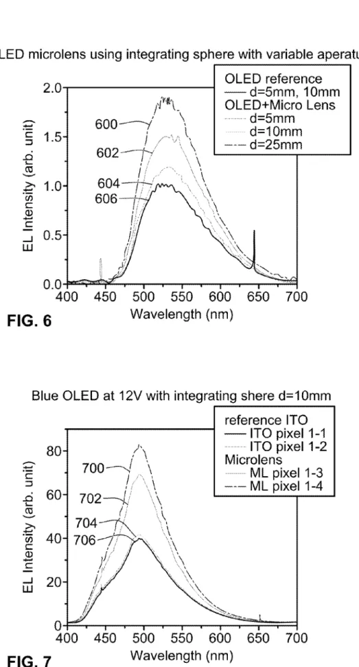
FIG. 6 is a graphic illustration of green OLED electrolu
minescence intensity measured with integrating sphere with
variable aperture;
FIG. 7 is a graphic illustration of blue OLED electrolumi
nescence intensity measured with integrating sphere; and
FIG. 8 is a schematic diagram of waveguided OLED emis sion modes resulting from total internal re?ection of a typical
OLED.
While the invention will be described in connection with certain preferred embodiments, there is no intent to limit it to
those embodiments. On the contrary, the intent is to cover all
alternatives, modi?cations and equivalents as included within the spirit and scope of the invention as de?ned by the
appended claims.
DETAILED DESCRIPTION OF THE INVENTION
Turning now to the drawings, embodiments of both the
manufacturing methods and resulting microlens arrays and
OLEDs incorporating same will be discussed. As will become apparent, embodiments of the present invention provide an
easy and cost effective method of making polymer-based microlens arrays with soft lithography. Indeed, preliminary
results of embodiments of OLEDs patterned with 1.5 pm diameter microlens arrays constructed in accordance with the
teachings of the present invention show 100% enhancement
of the electroluminescence (EL) output compared to conven tional ITO-coated glass-based OLEDs. This compares to the
largest enhancement reported to date discussed above, with 7
pm diameter microlens array, which is 68%.
In the conventional OLED geometry, once light is re?ected back into a waveguided mode, it can only escape as edge
emission, be absorbed by the waveguiding medium, or be
scattered. The microlens array can extract light in the guiding
mode in the substrate to a normal direction. This extraction
mechanism extracts more light not only in the light emitting
20 25 30 35 40 45 50 55 60 65
4
area but also outside of the light emitting area as long as there
is a guided light in the substrate as shown by FIG. 1. As shown in this FIG. 1, trace 100 illustrates the top emission of a
conventional OLED pixel and trace 102 the glass guiding
mode. However for a microlens covered OLED pixel, trace
104 illustrates top emission broadening and trace 106 illus trates the extra extraction from the guiding mode.
As such, extraction enhancement is governed by the area of the micro lens array patterned, as well as the period and dimensions of each microlens in the array. Embodiments of
the present invention have a large area of microlens array, e.g.
16x16 mm2, compared to the light emitting area, e.g. OLED
pixel area of 3.3><3 mm2. As will be discussed more fully
below, use of such large area microlens con?rms that extrac
tion is not restricted only to the pixel area of the OLED.
FIG. 2 shows a schematic diagram of one embodiment of
the microlens fabrication process of the present invention.
While preferred embodiments of this process and resulting apparatuses will utilize polyurethane (PU), those skilled in the art will recognize from the following that other optically transparent epoxies or polymers (OTE/P), e.g. SU-8, SU-8
2000, SU-8 3000 (collectively “SU-8”), Polydimethylsilox
ane (PDMS), Ormocers (Hybrid Polymers from Microresist
Technology, GmbH), polyacrylate (PA), NOA
61, 63 (Optical
Adhesives from Norland Inc.), etc., may be used in place of PU. As such, the following description should be taken by
way of example and not by way of limitation. As will also be
recognized by those skilled in the art, depending on which OTE/ P is utilized, the curing steps may be ultraviolet (UV) or thermally based as appropriate.
FIGS. 3A-D show scanning electron microscope (SEM) images of the patterns fabricated during the process of FIG. 2
in order to obtain the ?nal microlens pattern. FIG. 3A shows a 2D pattern of photoresist obtained by double exposure UV
laser interference holography, FIG. 3B metal-coated pattern for making spherical lens patterns, FIG. 3C PDMS molding,
and FIG. 3D stamping the pattern on the PU using the pat terned PDMS.
Soft lithography is used to create various structures with critical dimensions of a few microns. The advantages of the technique include ease of fabrication, large area structures, and very ordered and uniform patterns. With this method, a
structure may be generated with a PDMS mold that has an
identical relief pattern to that which is desired. Once the mold has been ?lled with a suitable material, it is simply stamped on any surface to create the pattern. Like all molds, the crucial step is to create the relief pattern that is the inverse of the structure to be generated. For feature size of a few microns, PDMS is an excellent choice because of its ?exibility and
non-wetting properties. Typically, PDMS is poured onto a
master stamp to create the relief pattern. After the PDMS is cured and solidi?ed, it is peeled off the master stamp and is ready to use. As long as the master stamp is not physically damaged, it can be used repeatedly for making more molds, which can also be used many times until damaged through
wear.
Returning to FIG. 2, the microlens arrays are fabricated on
the blank glass side of the OLEDs using PU as follows: The
master stamp is fabricated using two-beam laser holography
on a photoresist. Since a single exposure to UV light creates a 1-D pattern, a 2-D pattern is achieved by a second exposure
after rotating the sample by 90°. This results in an inverse
microlens pattern of photoresist 202 on a glass substrate 200
(see image of FIG. 3A). The bottom of the structure is not
quite as spherical as that for an optimal microlens but this is
remedied by heating the sample to 140° C. for 60 seconds.
US 8,742,406 B1
5
deposition of a 100 nm gold ?lm 204 on top of the photoresist 202 (see image of FIG. 3B). The gold ?lm 204 acts as an electrode for nickel electroplating. A total thickness of 10 pm
of nickel is electroplated (Caswell Plating) and the whole ?lm of nickel is detached from the glass substrate by dissolving
the photo-resist. This thin nickel sheet with the microlens
features facing up is carefully glued to a glass substrate 200'
for molding purpose. PDMS 206 is poured on top of the
master stamp and is peeled off after curing (see image of FIG.
3C). In one approach, a tiny drop of UV curable PU 208
(Summers Optical Type J-9l) is applied on the glass surface
of an ITO coated glass substrate 210 (Colorado Concept Coatings) and the PDMS mold 206 is pressed against it. Any excess PU is easily removed. Following this procedure, the
PU is cured in a UV chamber, the PDMS mold is lifted off,
and the microlens array is formed (see image of FIG. 3D). The
resulting structure may be seen in FIG. 4 illustrating the microlens array 412 on the ITO 414 coated glass substrate 410 for the OLED 416.
In one embodiment, the microlens array only covers a
portion of the ITO-coated glass as shown in FIG. 5. In this FIG. 5, an image of two OLED pixels is shown. A microlens
array is positioned above and around the left OLED pixel,
while no microlens array is included for the right OLED pixel as oriented in FIG. 5. Note that much of the edge emission
from the left pixel is absent from the left edge of its substrate
because it is extracted by the microlens array.
The ITO side of the glass is patterned and etched to form
the electrodes for multiple OLED pixels. Before the OLED pixel array is fabricated, the ITO glass is thoroughly cleaned with detergent and organic solvents and subsequently treated
in a UV ozone oven to adjust the ITO work function and
facilitate hole injection as is known. The organic layers, CsF,
LiF, or other buffer layer, and Al cathode are all thermally deposited in a vacuum evaporation chamber (background
pressure <5><10_6 ton) inside an Ar-?lled glove box. The organic layers consist of a hole injecting layer, typically cop per phthalocyanine (CuPc) or MoO3, a hole transport layer
(HTL), typically N,N'-diphenyl-N,N'-bis(l-naphthylphe
nyl)-l,l'-biphenyl-4,4'-diamine (NPD), an emitting layer of
any of various materials and blends, and an electron transport
layer (ETL), typically tris(8-hydroxyquinoline) Al(Alq3) or
4,7-diphenyl-l , l O-phenanthroline (BPhen).
Microlens embodiments of the present invention, as
examples, were used on two different emitting materials to determine effectiveness thereof. The two materials were
green light-emitting Alq3, and blue light-emitting 4,4'-bis(2,
2'-diphenylvinyl)- l , l'-biphenyl (DPVBi). Following deposi
tion of a l nm-thick LiF or CsF buffer layer, the ?nal Al
cathode layer is deposited through a shadow mask to yield
several 3 mm wide stripes. As a result, there are 8 OLED
devices on the ITO glass. Half of them are on the plain glass portion of the substrate and the rest are on the glass substrate
covered with the microlens array. The devices are encapsu lated after fabrication to protect them from expo sure to water
and oxygen and subsequent degradation. Wires are connected
to the electrodes of each pixel and to the power source for measurements. In this way, there can be a direct comparison
between the textured and plain glass substrates. Measure
ments are done by placing the device on the opening of an
integrating sphere. The signal collected in the integrating
sphere is transmitted through an optical ?ber to an Ocean
Optics spectrometer (Model Number S2000PCI) for analysis.
FIG. 5 shows the light intensity measurements of the emis
sive layer DPVBi from the micro-lenses textured area com
pared to the plain glass substrate. For simplicity, only two
devices on a plain glass substrate and a micro-lenses substrate
20 25 30 35 40 45 50 55 60 65
6
are shown. Because the contact resistance for each device is
different, the measurement intensity is normalized with the input power. It is clear that the devices behave identically except that the light extraction is signi?cantly higher from the
side coated with the microlens array. A similar result is achieved on a Pt octaethylporphyrin (PtOEP)-based guest
host emitting layer, although the enhancement is not as large
as that obtained with DPVBi.
In this FIG. 5, OLED pixels were fabricated under the same conditions with and without the microlens array. The same electric currents are applied to the two pixels. The area cov
ered with the microlens array has more broad extracted light even outside of the pixel area compared to the conventional
OLED which emits only above the (square) pixel area. The
edge emission can be observed around the OLED pixel array,
as it is sealed with, e. g., epoxy to avoid moisture contamina
tion and that epoxy seal scatters some of that edge emission towards the viewer. As clearly seen, the emission from the
edge of the microlens-covered left OLED pixel is much dim
mer than from that of the uncovered right pixel, demonstrat
ing that much of the waveguided light in the left pixel is
extracted by the microlens array as mentioned above. Note that the emission from the microlens-covered pixel is also
blurred. This might be useful in general lighting or backlight
ing in some electronic devices.
FIG. 6 shows the OLED intensities measured with a 3"
integrating sphere, to collect all the emission from the front
surface of the glass. As in FIG. 5, the reference pixel and the
pixel covered by the microlens array were from the same
array. Two types of OLEDs, with peak wavelength in the
green and blue bands, were tested separately. The OLED pixel size was ~3><3 mm2 and the microlens pattern area was ~15><15 mm2. The green OLEDs (FIG. 6) were placed on
opening ports of the integrating sphere of various sizes (trace
600 for d:25 mm, trace 602 for d:10 mm, trace 604 for d:5
mm). The reference pixel yielded same intensity regardless of
the opening size, whether 5 mm or 10 mm, as shown by trace
606, whereas the microlens array-covered pixel exhibited an
intensity increase of 100% with increasing collection area. The spectra of the blue OLEDs (FIG. 7) were measured with a ?xed opening size. Once again the micro lens array
increased the intensity by about 100%. The microlens pattern
was centered above one pixel (“pixel l”), and was off center
for another pixel (“pixel 2”) that pixel was effectively not covered directly by the microlens array.
When the pixels are placed in the middle of the opening of the integrating sphere, pixel l is covered by a larger area of the
microlens array pattern in comparison to pixel 2. The mea
surement using this con?guration indicates that extraction of the light waveguided in the glass is proportional to the micro
lens pattern area. Trace 700 illustrates ML pixel l-4, and trace 702 illustrates ML pixel l-3, whereas trace 706 illustrates the reference ITO pixel 1-1 and trace 704 illustrates reference
ITO pixel 1-2. This clearly demonstrates that the microlens array is extracting light from the substrate outside of the light
emitting pixel area and a large patterned area results in more
extraction as long as there is a waveguiding substrate. Embodiments of the invention are not limited to the OLED/
microlens materials and structures described above. For
example, embodiments of the OLEDs can be fabricated on a
plastic substrate, including directly on the (modi?ed) PU
microlens array. A mirror can also be included in an embodi
ment to re?ect the light that propagates in a direction opposite to the display direction. In another embodiment, the substrate
on which the OLED pixels are fabricated is beveled on both
US 8,742,406 B1
7
an embodiment. Encapsulated OLEDs are also subject to the
described outcoupling enhancement. lmportantly, as shown for green and blue OLEDs, mixed colors, such as red, green,
and blue are utilized on the same OLED pixel array to
enhance the outcoupling of all colors, including the resulting
mixed white light are also included. Microcavity OLEDs also bene?t from the outcoupling enhancement, and are also included.
All references, including publications, patent applications,
and patents cited herein are hereby incorporated by reference
to the same extent as if each reference were individually and
speci?cally indicated to be incorporated by reference and
were set forth in its entirety herein.
The use of the terms “a” and “an” and “the” and similar
referents in the context of describing the invention (especially
in the context of the following claims) is to be construed to cover both the singular and the plural, unless otherwise indi cated herein or clearly contradicted by context. The terms
“comprising,” “having,” “including,” and “containing” are to be construed as open-ended terms (i.e., meaning “including,
but not limited to,”) unless otherwise noted. Recitation of
ranges of values herein are merely intended to serve as a
shorthand method of referring individually to each separate
value falling within the range, unless otherwise indicated
herein, and each separate value is incorporated into the speci
?cation as if it were individually recited herein. All methods
described herein can be performed in any suitable order
unless otherwise indicated herein or otherwise clearly con
tradicted by context. The use of any and all examples, or
exemplary language (e.g., “such as”) provided herein, is
intended merely to better illuminate the invention and does
not pose a limitation on the scope of the invention unless
otherwise claimed. No language in the speci?cation shouldbe
construed as indicating any non-claimed element as essential
to the practice of the invention.
Preferred embodiments of this invention are described
herein, including the best mode known to the inventors for
carrying out the invention. Variations of those preferred
embodiments may become apparent to those of ordinary skill
in the art upon reading the foregoing description. The inven
tors expect skilled artisans to employ such variations as appropriate, and the inventors intend for the invention to be practiced otherwise than as speci?cally described herein. Accordingly, this invention includes all modi?cations and
equivalents of the subject matter recited in the claims
appended hereto as permitted by applicable law. Moreover,
any combination of the above-described elements in all pos
sible variations thereof is encompassed by the invention
unless otherwise indicated herein or otherwise clearly con
tradicted by context.
What is claimed is:
1. A light emitting device, comprising:
a light emitting pixel having a ?rst area;
a transparent electrode coupled to the light emitting pixel
and positioned on a ?rst surface of a transparent sub
strate;
an optically transparent epoxy/polymer (OTE/P) micro
lens array having a uniform pattern area larger than the
?rst area, the optically transparent microlens array posi
tioned on a second surface of the transparent substrate.
2. The light emitting device of claim 1, wherein the opti cally transparent microlens array is a polyurethane (PU)
microlens array.
3. The light emitting device of claim 1, wherein the micro
lens array includes a plurality of microlenses each having a diameter less than 7 pm.
20 25 30 35 40 45 50 55 60 65
8
4. The light emitting device of claim 3, wherein the diam
eter is approximately 1.5 pm.
5. The light emitting device of claim 1, wherein the ?rst
area is approximately 3><3 mm2 and the pattern area is at least
approximately 15x15 m2.
6. The light emitting device of claim 1, wherein the light
emitting pixel is an organic light emitting diode (OLED).
7. The light emitting device of claim 1, wherein the light
emitting pixel is a small molecular organic light emitting
diode (SMOLED).
8. The light emitting device of claim 1, wherein the light
emitting pixel is a polymer light emitting diode (PLED).
9. The light emitting device of claim 1, wherein the trans parent substrate is glass.
10. The light emitting device of claim 1, wherein the trans parent substrate is plastic.
11. The light emitting device of claim 1, wherein the trans
parent substrate is beveled on both sides of the light emitting
pixel.
12. The light emitting device of claim 1, further comprising a mirror positioned to re?ect light from the light emitting
pixel that propagates in a direction away from the microlens
array.
13. The light emitting device of claim 1, wherein the opti
cally transparent microlens array is one of an SU-8 microlens
array, a polydimethylsiloxane (PDMS) microlens array, an Ormocers microlens array, an polyacrylate (PA) microlens
array, an NOA 61 microlens array, or an NOA 63 microlens
array.
14. A method of manufacturing a light emitting device
having a light emitting pixel having a ?rst area attached to a
transparent substrate, comprising the steps of:
applying curable optically transparent epoxy/polymer
(OTE/ P) on a front viewing face of the transparent sub
strate of the light emitting device;
pressing a PDMS mold having a relief pattern of a micro lens array having an area greater than the ?rst area
against the curable OTE/P;
curing the curable OTE/ P;
removing the PDMS mold to form the microlens array on
the front viewing face.
15. The method of claim 14, wherein the steps of applying,
pressing, and curing, comprise the steps of:
applying one of UV curable polyurethane (PU), polyacry
late (PA), NOA 61, or NOA 63 on the front viewing face
of the transparent substrate of the light emitting device; pressing the PDMS mold against the UV curable PU, PA,
NOA 61, or NOA 63; and
curing the UV curable PU, PA, NOA 61, or NOA 63.
16. The method of claim 15, wherein the step of applying comprises the step of applying a drop of UV curable polyure
thane (PU) on a front viewing face of an indium tin oxide
(ITO) coated glass substrate of the light emitting device.
17. The method of claim 14, wherein the step of pressing
comprising the step of pressing a PDMS mold having a relief pattern of a microlens array including a plurality of OTE/P microlenses each having a diameter less than 7 pm.
18. The method of claim 14, wherein the step of pressing
comprising the step of pressing a PDMS mold having a relief pattern of a microlens array including a plurality of PU micro lenses each having a diameter of approximately 1.5 pm.
19. The method of claim 14, further comprising the step of
attaching a mirror to the transparent substrate such that light
from the light emitting pixel that propagates away from the front viewing face is re?ected.
US 8,742,406 B1
9
21. The method of claim 20, wherein the step of manufac
turing the PDMS mold comprises the steps of:
fabricating a master stamp inverse microlens pattern on a
glass substrate;
thermal depositing a gold ?lm on top of the master stamp
inverse microlens pattern;
electroplating nickel on the gold ?lm to form a patterned
nickel sheet;
detaching the patterned nickel sheet from the glass sub strate;
attaching the patterned nickel sheet to a glass substrate for
molding purpose;
pouring PDMS on top of the patterned nickel sheet;
curing the PDMS; and
peeling off the PDMS for use as the PDMS mold.
22. The method of claim 21, Wherein the step of fabricating
comprises the steps of using two-beam laser holography on a
photoresist by providing a single exposure to UV light to create a l-D pattern, rotating the photoresist by 90°, provid
ing a second exposure to UV light to create a 2-D pattern.
23. The method of claim 22, Wherein the step of detaching comprises the step of detaching the patterned nickel sheet
from the glass substrate by dissolving the photoresist.
24. The method of claim 21, further comprising the step of
heating the master stamp inverse microlens pattern to
approximately 140° C. for approximately 60 seconds.
25. The method of claim 21, Wherein the step of thermal
depositing a gold ?lm comprises the step of thermal deposit ing a 100 nm gold ?lm, and Wherein the step of electroplating
comprises the step of 10 pm of nickel on the gold ?lm.
26. The method of claim 14, Wherein the steps of applying,
pressing, and curing, comprise the steps of:
applying one of thermally curable SU-8, PDMS, or Ormocers on the front vieWing face of the transparent
substrate of the light emitting device;
pressing the PDMS mold against the thermally curable
SU-8, PDMS, or Ormocers; and
curing the thermally curable SU-8, PDMS, or Ormocers.
20
25
30
35
10
27. A method of increasing the extraction ef?ciency of an
organic light emitting diode having a light emitting pixel and
a transparent electrode coupled to the light emitting pixel and
positioned on a ?rst surface of a transparent substrate, com
prising the steps of:
positioning an optically transparent epoxy/polymer (OTE/
P) microlens array including a plurality of uniformly
patterned OTE/ P microlenses each having a diameter of
approximately 1.5 pm on a second surface of the trans
parent substrate.
28. The method of claim 27, Wherein the light emitting
pixel has a ?rst area, and Wherein the step of positioning comprises the step of positioning a OTE/P microlens array
having a pattern area larger than the ?rst area on the second
surface of the transparent substrate.
29. The method of claim 27, Wherein the step of positioning comprises the step of positioning a polyurethane (PU) micro
lens array including a plurality of PU microlenses each hav ing a diameter of approximately 1.5 pm on the second surface of the transparent substrate.
3 0. The method of claim 27, Wherein the step of positioning
comprises the step of positioning an SU-8 microlens array
including a plurality of uniformly patterned SU-8 micro
lenses each having a diameter of approximately 1 .5 pm on the second surface of the transparent substrate.
31. The light emitting device of claim 1, Wherein the opti cally transparent epoxy/polymer (OTE/ P) is either UV cur
able or thermally curable.
32. The light emitting device of claim 1, Wherein the opti
cally transparent epoxy/polymer (OTE/ P) microlens array is
fabricated using a PDMS mold having a relief pattern for a
microlens array formed therein.
33. The light emitting device of claim 1, manufactured
using the method of claim 14.