Design and Development of Single Input Multi
Output Flyback Converter Using Digital
Controller
Niveditha M, Karanam Vasudha, Durga Prakash, Satish S
M.Tech Student, Dept. of EEE, BNMIT, Visvesvaraya Technological University, Bengaluru, India
Assistant Professor, Dept. of EEE, BNMIT, Visvesvaraya Technological University, Bengaluru, India
Director, Dubas Engineering Pvt Ltd, Bengaluru, India
In charge of D & D Dept, Dubas Engineering Pvt Ltd, Bengaluru, India
ABSTRACT : A more efficient method of providing electrical isolation between input and output of a dc-dc converter is to use a transformer in the switching scheme. Flyback converter is one of the popular isolated DC-DC converter topology used to obtain regulated output voltage in low power application. The proposed project is aimed at the design and implementation of a high frequency, multiple outputs in a discontinuous mode with resonant switching for industrial applications.
The converter is operated at a switching frequency of 132 kHz using Digital Controller called Link switch which is a combination of MOSFET and PWM controller. The converter is validated with an experimental setup which delivers three outputs with desired efficiency of 80%. This proposed project is a implementation of single input and multiple output Flyback converter with MOSFET as switching device. Simulation is carried out with input of 120V DC and multiple output of one number of 18V, two number of 7V. The power rating is 30W. The prototype of the proposed converter is built. Prototype was conducted for 120VDC-400VDC input.
KEYWORDS : Flyback, DC-DC converter, Link-switch, Discontinuous mode, Resonant Switching.
I. INTRODUCTION
DC-DC converters are mainly used to provide required output voltage by suitably controlling the pulse width modulated (PWM) signal given to the gate of the acting power electronics switches. The main disadvantage of the basic DC-DC converters (Buck, Boost, Buck-Boost, Spic, Cuk) is electrical connection between the input and output. If the input supply is grounded, that same ground will be present on the output. This is overcome by isolating the output from the input electrically with a transformer. The isolated DC-DC converters are namely: Flyback Converter, Forward Converter, Half Bridge and Full Bridge Converters and Push-Pull Converter.
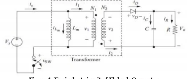
Figure 1: Equivalent circuit of Flyback Converter
A. Difference between continuous and discontinuous conduction Mode Flyback Converter
Continuous conduction mode (CCM) Discontinues conduction mode (DCM)
In CCM the diodes are not operated at zero current. DCM provides better switching conditions for the rectifier diodes, since the diodes are operating at zero current just before becoming reverse biased.
The transformer size can’t be reduced using CCM because the average energy storage is high.
The transformer size can be reduced using DCM because the average energy storage is low.
CCM is preferred for low voltage and high current output applications, because the RMS current is low, which decreases conduction loss of MOSFET and the current stress on the output capacitor.
DCM is recommended for high voltage and low current output applications, because the RMS current is high, which increases conduction loss of MOSFET and the current stress on the output capacitor.
In CCM fly-back converter, the design process is straight forward since the input-to-output voltage gain depends only on the duty cycle.
The input to output voltage gain of a DCM fly-back converter depends not only on the duty cycle but also on the load condition, which causes the circuit design to be somewhat complicated.
The main reason for using DCM Flyback converter is that, the stability is easier to achieve because at frequencies less than one half the switching frequency has no net inductance reflected to the transformer secondary, hence no second pole in the input to output transfer function and no right half-plane (RHP) zero appears as no energy is delivered to the output in each cycle which is directly proportional to the switching device on time in DCM case.
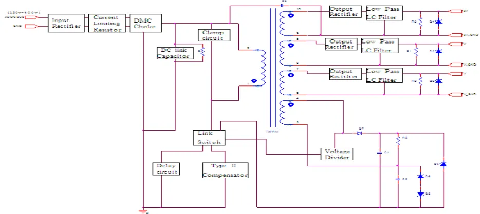
Figure 2. General block diagram
B. Proposed converter general block diagram
inrush current during start. Differential mode choke (DMC)input filter is used to neglect the differential noise present in the circuit, these differential noises are usually the commentary signals which cancel out each other and this circuit provides a known impedance at the input. The RCD snubber circuit is used to provide a path for leakage current produced due to leakage inductance usually used to avoid high dv/dt. A Transformer provides electrical isolation between primary and secondary winding. The flyback transformer is designed for an input of 120V to 400V dc with three secondary outputs of 18V, 7V and 7V. The Link switch (LNK6667E) is a digital controller which is an IC integrated with MOSFET as switching device and PWM controller on a single silicon chip. The output rectifier is used to convert the high frequency DC to a constant DC output voltage. A LC low pass Filter is used to filter high frequency components such as ripple and passes low frequency components (DC). The DC outputs are used to supply the load as per the application requirement.
II. MULTIPLE OUTPUT FLYBACK TOPOLOGY
The proposed converter as shown in Figure 3 has a similar operation as that of a conventional flyback converter during ON time of the switch, the energy is stored in the transformer and during OFF time the stored energy is transferred to the secondary circuit. A PWM signal is given to the MOSFET where both MOSFET and PWM controller are integrated on a single chip. This Single chip IC is called Link Switch (LNK6667E) which operates at the switching frequency of 132 kHz. The FEEDBACK pin in the Link switch is used to sense input and output voltage by sensing the auxiliary winding. During MOSFET ON-time the current out of FEEDBACK pin is used to sense the input voltage. During the OFF-time the FEEDBACK voltage is proportional to the output voltage through the turns ration between the secondary outputs and the FEEDBACK winding. The proposed converter is aimed at output voltages of 18V, 7V and 7V.
Figure 3: Block diagram of the proposed prototype
III. DESIGN CONSIDERATIONS
A. Flyback Converter
Sl.No Description Specifications
1 Output power rating 30W
2 Input voltage range 120-400Vdc
3 Switching frequency 132kHz
4 Vout1 18V
5 Vout2 7V (2 no’s)
6 Voltage consideration for bias voltage 12V
TABLE I: Flyback converter Parameters
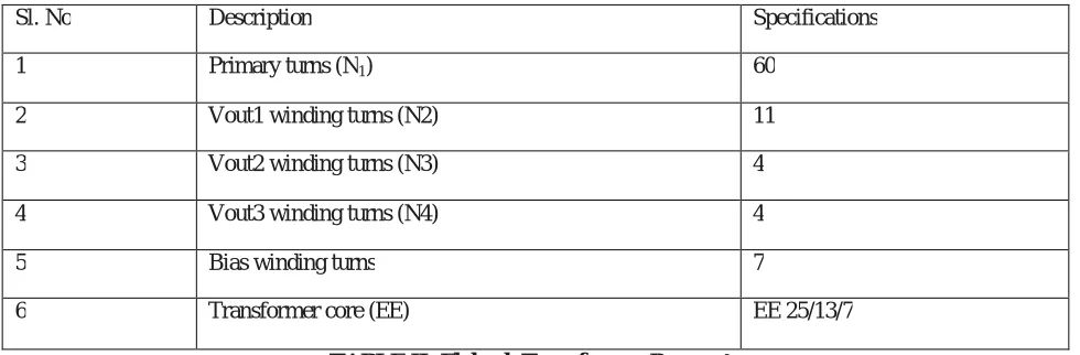
C. Flyback Transformer
Table II Shows the Flyback transformer parameter considered for the designed converter circuit. The transformer design is carried out. During Flyback converter operation, when the switch is on, input dc voltage appears across the transformer primary winding. When the switch is off reflection voltage (V1) can be seen across primary winding of the transformer.
Sl. No Description Specifications
1 Primary turns (N1) 60
2 Vout1 winding turns (N2) 11
3 Vout2 winding turns (N3) 4
4 Vout3 winding turns (N4) 4
5 Bias winding turns 7
6 Transformer core (EE) EE 25/13/7
TABLE II: Flyback Transformer Parameters
C. Current Mode Digital Controller
Linkswitch (LNK6667E) Current mode controller mainly used to obtain regulated output voltage with peak current limit capability in offline DC-DC Converter. This is a digital controller switch with combination of MOSFET and PWM controller which gives extensive protection like auto-restart during overload faults, output short circuit protection, accurate thermal shutdown, line over voltage shutdown extends line surge withstanding line brown-in/out protection and in addition to this it has a feedback winding which is used to sense output and input voltage by sensing the auxiliary winding voltage.
in DSon
I
R
loss
Conduction
2fall sw pk
DC
I
f
T
V
oss
Switchingl
oss
Switchingl
loss
Conduction
Totalloss
D. RCD Clamp Circuit
rise in voltage by suitably absorbing leakage energy. The voltage rating of diode should be greater than the DC bus voltage.
E. Rectifier Diode and Capacitor Selection
Rectifier diode selection depends on the peak inverse voltage (VR) across it and output current.
S
R
PIV
V
1
.
25
Where ID is the diode rated DC current is the average output current which depends on the thermal rise in duration of peak load condition.
O
D
I
I
3
O O O
V
P
I
Output capacitor selection depends on the ripple current.
2 2
av rms rippleI
I
I
With low ESR an electrolytic capacitor is selected.
Output ripple voltage is
I
SP
ESR
the capacitor rating is increased on the basis of measured capacitor temperaturerise under worst case loading and ambient temperature. ESR of the capacitor is multiplied with the secondary peak current to give the switching ripple voltage. Therefore it is important to select the low ESR capacitor to reduce the ripple voltage. Usually, selecting a high ripple current rated capacitor results in a acceptable value of ESR.
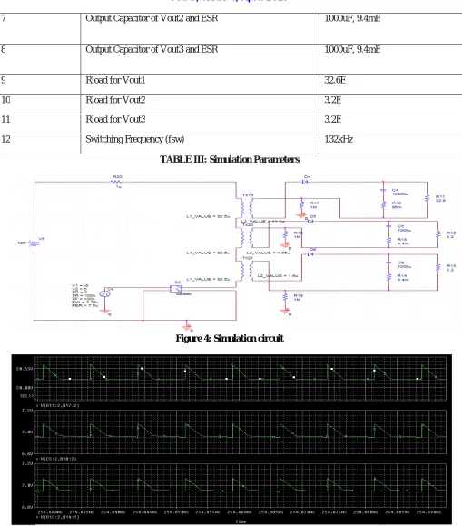
IV. SIMULATION
The triple output flyback converter topology is simulated using Orcad Pspice software.
The simulation parameter is shown in the Table III. The simulation model includes linear transformer, VDC Source, Vpulse and SBreak (ideal switch) at the input side. D1, D2 and D3 are the rectifier diodes. C1, C2 and C3 are the output capacitor across the regulated output of Vout1, Vout2 and Vout3 for an DC input of 120V. The PWM pulse required for SBreak is given by the Vpulse with the required duty cycle for the given switching frequency. The simulation circuit is shown in Figure 4 and Simulation results are shown in Figure 5.
Sl. No Description Specifications
1 Primary inductance (L1) 60uH
2 Output inductance Vout1 (L2) 11.1uH
3 Output inductance Vout2 (L2) 1.55uH
4 Output inductance Vout3 (L2) 1.6uH
5 VDC Voltage 120V
7 Output Capacitor of Vout2 and ESR 1000uF, 9.4mE
8 Output Capacitor of Vout3 and ESR 1000uF, 9.4mE
9 Rload for Vout1 32.6E
10 Rload for Vout2 3.2E
11 Rload for Vout3 3.2E
12 Switching Frequency (fsw) 132kHz
TABLE III: Simulation Parameters
Figure 4: Simulation circuit
V. HARDWARE IMPLEMENTATION AND RESULTS
The proposed converter is implemented in the hardware as discussed in earlier section; the hardware setup is shown in Figure 6 and Figure 7. Controller generates initial PWM signal. Thus by switching action flyback converter provides 18V and two 7V outputs for input voltage ranging from 120V to 400 V with switching frequency of 132 kHz and output power rating of 30W. A separate feedback winding is used to provide 5.6V as bias supply for the controller. Protection circuit such as snubber is used.
Figure 6: Hardware built on GPCB Figure 7: Hardware Setup
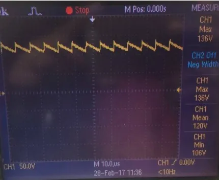
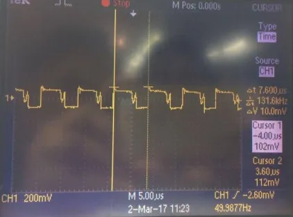
The experiment was carried out for DC input voltage of 300V with Rload (Rload1= 33E, Rload2 = 3.3E and Rload3 = 3.3E). The hardware results are shown in Figure 8, Figure 9, Figure 10, Figure11 and Figure 12.
Figure 10: Secondary output voltage 2(Vout2) of 7.11V Figure 11: Secondary output voltage 3(Vout3) of 7.66V
Figure 12: Duty cycle and switching frequency
VI. CONCLUSION
The multiple output flyback converter is designed to operate in the wide input range of 120V to 400V. The hardware prototype is build and the results are captured. The converter is observed to have ripple voltage less than 1% with good output regulation.
The use of link switch in the circuit reduces conduction and switching losses, reduction is component count. Thus, resulted in higher efficiency for lower input voltage and higher reliability.
REFERENCES
1. Nagesha C and A Sreedevi, “Simulation and Hardware Implementation of 24Watt Multiple Output Flyback Converter”, 2015
International Conference on Power and Advanced Control Engineering (ICPACE).
2. K.V.S Mourya Chandra and Ravishankar Deekshit “Design and Implementation of Current Mode Controlled Multi-Output Flyback
Converter for Military Application” 2015, IEEE International conference of Electronics, Computing and Communication technologies
(CONECCT).
3. Li-Yuan Liao, Adbullah Sani, Yao-Ching, Yao-Ching Hsieh, Jing-Yuan Lin and Huang-Jen Chiu “High Step-up Forward Flyback
Converter with Parallel Output” 2016, IEEE International Conference on Industrial Technology (ICIT).
4. N.Vazquez, H.Lopez, C.Hernandez, H.Calleja“Multiple Output DC-to-DC based on the Flyback Converter” 2008, 11th IEEE International
5. Jianting Li “A High-Switching-Frequency Flyback Converter in Resonant Mode” 2016, IEEE Transactions on Power Electronics.
6. Suprabha Padiyar U, Vedavyasa Kamath “Design and Implementation of a Universal Input Flyback Converter” 2016, International
Conference on Electrical, Electronics, and Optimization Techniques (ICEEOT).
7. Mauro Andre Pagliosai, Rafeal Gomes Faust, Telles Brunelli Lazzarin and Ivo Barbi “Input-Series and Output-Series Connected Modular
Single Switch Flyback Converter Operating in the Discontinuous Conduction Mode”.
8. Prasanth Thummala, Henrik Schneider, Zhe Zhang and Michael A.E. Andersen “Bidirectional Flyback Converter with Multiple Series
Connected Outputs for High Voltage Capacitive Charge and Discharge Applications” 2015, IEEE Applied Power Electronics Conference