Highly Efficient Design of DSP Systems Using
Electronic Design Automation Tool to Find
Iteration Bound
G. S. Satish KumarM.Tech SP&VLSI, Department of Electronics and Communication, Jain University, Bangalore Email: [email protected]
Hari Krishna Moorthy
Asst. Professor, Department of Electronics and Communication, Jain University, Bangalore Email : [email protected]
---ABSTRACT--- Digital signal processing algorithms are repetitive in nature. These algorithms are described by iterative data flow graph (DFG) where nodes represent tasks and edges represent communication. Execution of all nodes of the DFG once completes iteration. Successive iteration of any node are executive with a time displacement referred to as the iteration period. For all recursive signal processing algorithms, there exists an inherent fundamental lower bound on the iteration period referred to as the iteration period bound or the iteration period. This bound is fundamental to an algorithm and is independent of the implementation architecture. In other words it is impossible to achieve an iteration period less than the bound even when infinite processors are available to execute the recursive algorithm. Iteration bound need to be determined in rate-optimal scheduling of iterative data flow graph. The iteration bound determination has to pre-order repeatedly in the scheduling phase of the high level synthesis. In recursive constrained scheduling a given processing algorithm is scheduled to achieve the minimum iteration period using the given hardware resources. In order to execute operation of the processing algorithm in parallel, the required number of processors or functional units required to execute the operation in parallel may be larger than the number of available resources. Generally the precedence to be assigned is not unique. Hence the iteration bound should be determined for every possible precedence to check which precedence leads to the final schedule with the minimum iteration period. Consequently the iteration bound may have to be computed many times and it is important to determine the iteration bound in minimum possible time.
Keywords – DSP Algorithms, DFG, Iteration Bound, LPM, MCM.
---
Date of Submission: 01-09-2012 Date Revised: 02-09-2012 Date of Acceptance: 09-09-2012
---
1.INTRODUCTION
D
igital signal processing(DSP) is used in numerousapplication such as video compression, portable video system computers, digital audio, multimedia and wireless communication systems, radar imaging, acoustic beam forming, global positioning system, biomedical signal processing. The field of DSP has always been driven by the advance in DSP application and in scaled VLSI technologies. Therefore at any given time, DSP applications impose several challenges on the implementation of the DSP system. These implementations must satisfy the enforced sampling rate constraints of the real time DSP applications and must require less space and power consumption.
Methodologies needed to design custom or semi-custom VLSI circuit for these applications. DSP computation is different from general purpose computation in the sense that DSP programs are non- terminating program. In DSP computation, the same program is executed repetitively on an infinite time series. The non-terminating nature can be
exploited to design more efficient DSP system by exploiting the dependency of tasks both within iteration and among multiple iterations.
Furthermore long critical path in DSP algorithms limit the performance of DSP system. These algorithms need to be transformed for design or “high speed” or “low-area” or “low-power” implementation. VLSI DSP is field of design efficient architecture, algorithms and circuit, which can be operated with either less area or power consumption or with higher speed or lower round off noise. High level architectural transformation that can be used to design families of architectures for a given algorithm. These transformation include ‘pipelining’ ‘Retiming’ ‘unfolding’ ‘Folding’ and ‘systolic array’ design methodology.
one to one mapping of algorithm operations to processors. Thus it is important to know the design technologies not just to a single architecture but a family of architecture out of which an appropriate architecture can be selected for a specific purpose.
Two important features that distinguish DSP from other general purpose computations are the
•Real time throughput requirement.
•Data driven property.
The hardware should be designed to meet the tight throughput constraint of the real time processing where new input samples need to be processed as they are received periodically from the signal source as opposed to first storing them in buffers and then processing them in batch mode. If the throughput of a system is less than the required sample rate, the new inputs need to be stalled (or buffered), which requires an infinite length buffer. However, once the sample rate is met by the hardware, there is no advantage in making the computation any faster.
The second important attribute of signal processing systems is its data driven property, implied by the fact the any subtasks or computations in a DSP system can be performed once all the input data are available. In the sense, these systems are synchronized by the flow of data, instead of the system clock. This enables the use of asynchronous circuit for DSP system where no global clock is required.
2.DSPALGORITHMS
DSP algorithms are described by non-terminating programs which execute the same code repetitively. For example, a 3-tap FIR digital filter described by the non-terminating program.
y(n)=ax(n)+bx(n-1)+cx(n-2); for n=1 to n=α (1) Execution of all the computations in the algorithms once is referred to as iteration. The iteration period is the time required for execution of an iteration of the algorithm. The iteration rate is the reciprocal of the iteration period. During each iteration, the 3-tap FIR filter equation (1) above processes one input signal, completes 3 multiplication and 2 addition operations (in serial or in parallel), and generates one output sample. DSP systems are also characterized by the sampling rate (also referred to as throughput) in terms of number of samples processed per second. The critical path of a combinational logic circuit is defined as the longest path between inputs and out puts, where the length of a path is proportional to its computation time. DSP systems generally are implemented using sequential circuits, where the critical paths are defined as the longest path between any two shortage elements (or delay elements). The critical path computation time determines the minimum feasible clock period of DSP system. The latency is defined as the difference between the time an output is generated and the time at which its corresponding input was received by the system.
For system containing combinational logic only, latency is usually represented in terms of absolute units, or the number of gate delays; for sequential systems, latency is usually represented in terms of number of clock cycles. Generally, the clock rate of a DSP system is not the same as its sampling rate. DSP algorithms are described using mathematical formulations at a higher level where it is more important to specify the functionality of the system than the order and structure of the internal operations. For architectural design, these mathematical formulations need to be converted to behavioral description languages or graphical representations.
The behavioral description languages include applicative languages, prescriptive languages, and descriptive languages. The applicative languages represent a set of equations that are satisfied by the variables in the algorithm, rather than a sequence of actions (assignments to be carried out, i.e., the order of the assignment statements is not important). Applicative languages are popular for the description of DSP systems. The prescriptive languages explicitly specify the order of the assignment statements some examples of these types of languages include high level programming languages such as Pascal, c, or fortan. More recently, many applications are being defined using descriptive languages that represent the structure of a DSP system. Examples of these are the hardware description languages such as verilog or VHDL.
Graphical are efficient for investigating and analyzing data flow properties of DSP algorithms and for exploiting the inherent parallelism among different subtasks. More importantly, graphical representations can be used to map DSP algorithms to hardware implementations. Hence, these representations can bridge the gap between algorithmic descriptions and structural implementations. The absolute measure of the performance metrics of DSP systems, area, speed, power, and round off noise cannot be obtained without the knowledge of the supporting technology in which the system is implemented. However, the graphical representations exhibit all the parallelism and data-driven properties of the system, and provide insight into space and time trade-offs. With graphical representations, the architectural design space can be explored and an appropriate architecture can be selected in a technology-independent manner.
explore architectural alternatives using high-level transformations.
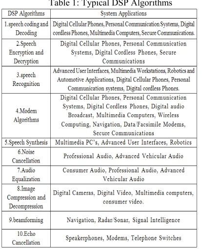
Table 1: Typical DSP Algorithms
3.ITERATIONBOUND
Many DSP Algorithms such as recursive and adaptive digital Filters contain feedback loops, which impose an inherent fundamental lower bound on the achievable iteration or sample period. This bound is Referred to as the iteration period bound, or simply the iteration bound. The iteration bound is a characteristic of the representation of an algorithm in the form of a data flow graph (DFG). Different representation of the same algorithm may lead to different iteration bound. It is not possible to achieve an iteration period less than the iteration bound even when infinite processors are available.
A DSP program is often represented using a DFG, which is a directed graph (i.e. each edge has a distinct direction) that describes the program. DFG consists of a set of nodes and edges. The edges represented communication between the nodes, and each edge has a nonnegative number of delays associated with it. An iteration of a node is the execution of the node exactly once, and an iteration of the DFG is the execution of each node in the DFG exactly once. Each edge in a DFG describes a precedence constraint between two nodes. This precedence constraint is an intra-iteration precedence constraint if the edge has zero delays or an inter-iteration precedence constraint if the edge has one or more delays. Together, the intra-iteration and inter-iteration precedence constraints specify the order in which the nodes in the DFG can be executed.
A DFG can be classified as non-recursive or recursive. A non-recursive DFG contains no loops, while a recursive DFG contains at least one loop. A recursive DFG has a
fundamental limit on how fast the underlying DSP program can be implemented in hardware. This limit, called the ‘iteration bound’ T∞, holds regardless of the computing power available for the implementation of the DSP program.
In other words, the loop bound of the critical loop is the iteration bound of the DSP program, which is the lower bound on the iteration or sample period of the DSP program regardless of the amount of computing resources available. Number of loops in a DFG can be exponential with respect to the number of nodes.
To compute iteration bound in polynomial time, two algorithms will be developed
• Longest path matrix algorithm
• Minimum cycle mean algorithm
3.1 A. DATA-FLOW GRAPH REPRESANTATION
DSP programs are considered to be non-terminating programs that run from time index n=0 to time n=∞.For example, a DSP program that computes Y(n)=aY(n-1)+X(n) represents the following program:
For n=0 to ∞, Y(n)=aY(n-1)+X(n) (2)
Fig. 1 Graphical representation
Fig. 2 Data Flow Graph
(The numbers in parentheses are the execution times for the nodes)
T he input to this DSP program is the sequence X (n) for n=0, 1, 2, . . . . and the initial condition Y(-1). The output is the sequence Y (n) for n=0, 1, 2, . . . .
A DSP program is often represented using a DFG, which is a directed graph (i.e., each edge has distinct direction) that describes the program. For example, the program Y(n)=aY(n-1)+X (n) is graphically represented in fig 1. A simplified version of this program is shown in fig 2. The structure in fig 2 is a DFG, which consists of a set of nodes and edges.
edge AB has zero delays and the edge BA has one delay. An iteration of a node is the execution of the node exactly once, and an iteration of the DFG is the execution of each node in the DFG exactly once. Each edge in a DFG describes a precedence constraint between two nodes. This precedence constraint is an intra-iteration precedence constraint if the edge has zero delays or an inter-iterations precedence constraint if the edge has one or more delays. Together, the intra-iteration and inter-iteration precedence constraints specify the order in which the nodes in the DFG can be executed.
The edge from A to B in fig 2 enforces the intra-iteration
precedence constraint, which states that the k-th iteration of
A must be executed before the k-th iteration of B. The edge
from B to A enforces the inter-iteration precedence constraint, which states that the k-th iteration of B must be
executed the (k+1)-th iteration of A. Let X
k denote the k-th
iteration of the node X. When it is important to distinguish between intra-iteration and inter-iteration precedence constraints, an intra-iteration precedence constraint is
denoted using a single arrow such as AkBk and inter-
iteration precedence constraint is denoted using a double
arrow such as Bk=Ak+1. Otherwise, all precedence
constraints are denoted using single arrows. The critical path of a DFG is defined to be the path with the longest computation time among all paths that contain zero delays.
The critical path in the DFG in fig 2 is the path AB,
which requires 6 u.t. The DFG in fig 3 contains several paths with no delays. The maximum computation time
among these paths is 5 u.t.(the two paths 6321 and
5321 are both critical paths), so the critical path
computation requires 5 u.t. The critical path is the longest path for combinational rippling computation time for 1 iteration of the DFG.
A DFG can be classified as non-recursive or recursive. A non-recursive DFG contains no loops, while a recursive DFG contains at least one loop. For example, an FIR filter is non-recursive, while the DFG in fig 3 is recursive
because it contains the loop ABA. A recursive DFG
has a fundamental limit on how fast the underlying DSP program can be implemented in hardware. This limit, called the iteration bound T∞ [1][2], holds regardless of the computing power available for the implementation of the DSP program.
Fig. 3 A DFG with three loops that have loop bounds of 4/2 u.t.,5/3 u.t., and 5/4 u.t. The iteration bound for this DFG is T∞=2 u.t.
A straightforward technique for finding the iteration bound of a DFG is to locate all loops and directly compute T∞ using (3); however, the number of loops in a DFG can be exponential with respect to the number of nodes, so this technique can require long execution times. Three techniques have been developed for computing T∞ in polynomial time, namely the longest path matrix algorithm, the minimum cycle mean algorithm, and the negative cycle detection algorithm.
4.ALGORITHMSFORCOMPUTING ITERATIONBOUND
The two iteration-bound algorithms described in this section are demonstrated using the DFG in fig 3. This DFG
has three loops: L1 = 1421 with loop bound 4/2 u.t.,
loopL2= 15321 with loop bound 5/3 u.t., and loop
L3=16321 with loop bound 5/4 u.t. Therefore, the
iteration bound of this DFG is
T∞=max {4/2, 5/3, 5/4}= 2 u.t.
4.1 Longest path matrix algorithm
In the longest path matrix (LPM) algorithm, a series of matrices is constructed, and the iteration bound is found by examining the diagonal elements of the matrices. Let d be
the number of delays in the DFG. These matrices, L(m) , m=
1, 2, ……. , d, are constructed such that the value of the element, l (m,i,j) is the longest computation time of all
paths from delay element di to delay element dj that pass
through exactly m-1 delays (not including di and dj). If no
such paths exists, then l(m,i,j)=-1. Note that longest path between any two nodes can be computed using any path algorithms (bellman-ford, floyd-warshall algorithms). For example, to determine l (1,3,1) for the DFG in fig 3, all
paths from the delay element d3 to the delay element d1 that
pass through exactly zero delay elements must be
considered. There is one such path, namely, the path d3
n5 n3 n2 n1 d1. This path has computation time
5, so l(1,3,1)=5. To determine l(1,4,3), we note that there
are no paths from the delay element d4 to the delay element
d3 that pass through zero delay elements, so l(1,4,3)=-1.
After determining the rest of the elements of L(1) , we find
L( 1 )=
The higher order matrices, L(m) , m= 2, 3, ….., d, do not
need to be determined directly from the DFG. Rather, they can be recursively computed according to the rule
L((m+1), i, j) = max (-1, l (1,I, k)+l(m, k, j)),
k€K (4.1)
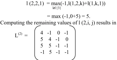
Where K is the set of integers k in the interval [1,d] such that neither l (1,I, k)=-1 nor l (m, k, j)=-1 holds. For example, to compute l (2,2,1), the first step is to find the set K from the possible set {1, 2, 3,4}. The value 3 is in K because l (1,2,3)=0 and l (1,3,1)=5, and the values k=1, 2, 4 are not in K because at least one of l(1,2,k) or l(1,k,1) is
equal to -1 for each of these. Using K={3}, the value of l (2,2,1) can be computed as
l (2,2,1) = max(-1,l(1,2,k)+l(1,k,1))
k€{3}
= max (-1,0+5) = 5.
Computing the remaining values of l (2,i, j) results in
L(2) =
…………(4.3)
While L(2) is computed using only L(1) , the matrix L(3)
is computed using both L(1) and L(2) .To compute l (3,3,3),
K={1} because l (1,3,1)=5 and l (2,1,3)=0, and for the values of k=2,3,4, at least one of l (1,3,k) or l (3,k, 3) is equal to -1. The value of l (3,3,3) is
l (3,3,3) = max (-1,l(1,3,k)+l(2,k,3))
k€{1}
= max (-1,5+0)=5.
Computing the rest of L(3) and L(4) results in
L(3) =
………(4.4)
And
L(4) =
..…………(4.5)
Once the matrices L(m) have been computed, the iteration
bound can be determined as
T∞ = max {l (m, i, i)/m}
i,m€{1,2,….d} (4.2)
Which for this example is
T∞= {4/2, 4/2, 5/3, 5/3, 5/3, 8/4, 8/4, 5/4, 5/4} = 2
The LPM algorithm works because the value l (m, i, i) represents the longest computation time of all loops that
have m delays and contain the delay element di. By taking
the maximum of l (m, i, i)/m for all possible values of I and m, we find the maximum loop bound of all loops in the DFG, which is the iteration bound.
The time complexity of computing L(k+1) from L(1) and
L(k) is O (d3) since there are d2 elements in L(k+1) and each
computation has time complexity O (d). Therefore,
computing L(d) from L(1) has time complexity O(d4).
Although we determined L(1) by inspection, an algorithm
with time complexity O(de) is given in above for finding
L(1) , where d and e are the number of delays and edges in
the DFG, respectively. Hence, the time complexity of the
LPM algorithm of computing the iteration bound is O(d4
+de).
4.2 The minimum cycle mean algorithm
The minimum cycle mean (MCM) algorithm reduces the problem of determining the iteration bound to the problem of finding the MCM of a graph. Here we compute the MCM efficiently by using below technique. Recall the terms ‘cycle’ and ‘loop’ can be used interchangeably.
The algorithm described in this section uses the concepts of cycle mean, the maximum cycle mean, and the MCM. The cycle mean m(c) of a cycle c is the average length of the edges in c, which can be found by simply taking the sum of the edge lengths and dividing by the number of edges in
the cycle. The MCM λmin is simply the minimum value of
all of the cycle means, i.e.,
λmin = mincm(c). (4.3)
Similarly, the maximum cycle mean λmax is
λmax = maxc m(c) (4.4)
Fig. 4 The graph Gd for the DFG in Fig. 3
Fig. 5 The graph Gd
The cycle means of a new graph Gd are used to compute
the iteration bound, where Gd can be found from the DFG
for which we are computing the iteration bound (call this DFG G). If d is the number of delay elements in G, then the
graph Gd has d nodes where each node corresponds to one
of the delays in G. The weight w (i,j) of the edge from the
node I to the node j in Gd is the longest path length among
all paths in G from the delay di to the delay dj that do not
pass through delays. If no zero-delay path exists from the
delay di to the delay dj, then the edge i j does not exist in
Gd .
The graph Gd for the DFG in Fig 3 is shown in Fig 4.
Note that constructing Gd is essentially the same as
constructing the matrix L1 in the LPM algorithm discussed
above.
The sum of the edge weights in a cycle c in the in the Gd
is the maximum computation time of all cycles in G that contain the delays represented by the nodes in the cycle c.
This is because the edge weights in Gd are the maximum
computations times between the delays in G. For example 4 -1 0 -1
5 4 -1 0 5 5 -1 -1 -1 5 -1 -1
5 4 -1 0 8 5 4 -1 9 5 5 -1 9 -1 5 -1
there are two cycles that contains the delays Dά and Dβ in the graph G in Fig 6, and these cycles have computation
times of 6 u.t. and 4 u.t. The corresponding graph Gd in fig
7 has one cycle that passes through the nodes corresponding
to Dα and Dβ. The sum of the edge weights in this cycle is 6,
which is the maximum computation time of two cycles in G
in fig 6. In Gd,, the number of edges in a cycle equals the
number of nodes in the cycle, and this equals the number of delays in the cycle in G. Therefore, the cycle mean of a cycle c in
Max computation time of all cycles Gd = in G that contain the delays in c
The number of delays in these cycles in G
This is the maximum cycle bound of the cycles in G that contain the delays in the cycle c. The maximum cycle mean
of Gd is the maximum cycle bound of all cycles in G,
which is the iteration bound of G.
Fig. 6 A graph G with two cycles that contain the delays Dœ and Dß
To compute the maximum cycle mean of Gd, the graph
Gd is constructed from Gd by simply multiplying the
weights of the edges by -1, i.e., Gd has the same topology
as Gd and the weights w(i,j) of the edge ij in the Gd are
given by w(I,j)=-w(I,j), where w(I,j) is the weight of edge
ij in Gd . The graph Gd for the DFG in Fig 3 is given in
Fig 4. The maximum cycle mean of Gd is simply the MCM
of Gd and multiplying it by -1.
Fig. 7 The Corresponding graph Gd
The MCM of Gd is found by first constructing the series
of d+1 vectors, f(m),m=0,1,….d, which are each of
dimension dX1. An arbitrary reference node is chosen in Gd
(call this node s). The initial vector f(0) is formed by setting
f(0)(s)=0 and setting the remaining entries of f(0) to α. If
node 1 is chosen as the reference node for the graph Gd in
Fig 4, then
0 f(0) = α
α α
The remaining vectors, f(m),m=1,2,,….d are respectively
computed according to
f(m)(j)= min(f(m-1)(i)+w(i,j))
i∈I
where w(i,j) is the weight of the edge ij in Gd and I is the
set of nodes in Gd such that there exists an edge from node i
to node j (i j) . This series of vectors found from Gd in
Fig 4 is
f(1) = f(2) =
f(3)= f(4) =
Table 2: Values of f(4)(i)-f(m)(i)
4-m for 1<=I<=4 and 0<=m<=3
For example, f(4)(1) is computed as
f(4) (1)= min( f(3) (2)-w(2,1) , f(3) (3)-w(3,1) , f(3) (4)-w(4,1))
= min(-4,-4,∞-5,0-5) = -8.
From the vectors f(m) , m= 0,1,2….d the iteration bound can
be computed as
T∞=-mini∈{1,2,…..,d} max f(d)(i)-f(m)(i)
m∈{0,1,….d-1} d-m
in our example, d=4,
Table 2 shows the values of
f(4)(i)-f(m)(i)
4-m
For 1≤i≤4 and 0 ≤m ≤3. In some cases we may encounter
f(d)(i)-f(m)(i)= ∞-∞. In this case ∞-∞ should be treated as
zero. For example, f(4)(4)-f(1)(4)= ∞-∞, so the value
(∞-∞)/3=0/3=0 is given for i=4 and m=1 as shown in the Table 2.
T∞=-min {-2, -1, -2, ∞}=2
M=0 M=1 M=2 M =3 Max0<=m<=3
f(4)(i)-f(m)(i)
4-m
I=1 -2 -α -2 -3 -2
I=2 -α -5/3 -α -1 -1
I=3 -α -α -2 -α -2
I=4 Α –α α –α α –α α Α -8
-5 -4 ∞ -5
-4 ∞ 0
-4 ∞ 0 ∞ ∞
5.RESULTS
5.1 Longest path matrix algorithm technique
In the longest path matrix (LPM) algorithm, a series of matrices is constructed, and the iteration bound is found by examining the diagonal elements of the matrices. As explained in the earlier section, we get the LPM output as shown below.
The required result iteration bound for the above DFG is obtained as shown below.
Step 1: Get the Menu using GUI command:
Here, the menu pops up with all the options required for the project analysis.
Step 2: Click the circuit file tab:
Here, the input data circuit tab appears, where we enter input.
Step 3: Enter the input:
Here the input itdata1 is the m.file which has the input DFG (shown in fig. 3) in the form of matrix.
Step 4: Click the ITB using LPM algorithm tab.
After the above step, we get a connection matrix corresponding to the DFG of the circuit. It has the formation of the tree branch where the starting node
Fig. 8 GUI for the whole module
is any delay element and terminated with any other delay element and without having any delay element in between. Step 5: The Iteration Bound is found as shown below (fig. 9)
Thus the 1st technique is used as shown above for the input
1.
Fig. 9 Iteration bound result for input 1, using LPM algorithm
5.2. Minimum cycle mean algorithm technique
The minimum cycle mean (MCM) algorithm reduces the problem of determining the iteration bound to the problem of finding the MCM of a graph. Here we compute the MCM efficiently by using the technique as explained in the section 4. Recall the terms ‘cycle’ and ‘loop’ can be used interchangeably.
5.3 Multi rate to single rate synthesis
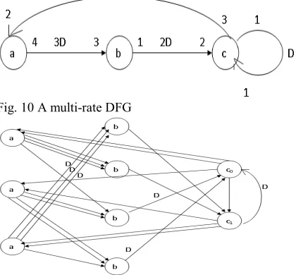
As explained in the section 4, the step two is used to compute the iteration bound of Multi rate DFG. The process is to construct a SRDFG that is equivalent to the MRDFG & Compute the iteration bound of the equivalent SRDFG using the LPM algorithm, or the MCM algorithm.
Here the input mrdfg1 is the m.file which has the input DFG (shown in fig 10) in the form of matrix and the k values as explained in the section 4.
Fig. 10 A multi-rate DFG
Fig. 11 An equivalent SRDFG for the MRDFG in fig 10
The equivalent SRDFG is used as the input in the matrix format and the edges are reduced using edge degeneration algorithm, which will not alter the output iteration bound. The table 5.1 below shows the number of edges reduced after using the algorithm.
Table 3
Total Number of edges before edge
degeneration
24
Number of edges after edge degeneration
16
Total decrease in percentage = [100-{(16/24)*100}]
= 33.33%
6.CONCLUSION
At present the challenge of designer is developing the complex algorithms in the chip is a very tedious task, reason is it has to meet the specification requirements. For one particular purpose there are number of algorithms which could complete the task but there is no information available about how much speed maximally we can achieve if these algorithms applied to the physical realization.
corresponding to pick up algorithms. Not only that if there is a requirement of enhancement of the speed in future, this can be taken care at the beginning itself and as a result cost effective solution can be generated within the short period. There are number of applications where multi rate circuit is being used, it is difficult to analyze such kind of the multi rate system. Tool has been developed in the presented work to synthesize the multi rate circuit by the single rate even with the quality of having less number of edges. It is expected that proposed solution will provide the help to researchers and professionals who wants to have the best speed facility in the circuit.
Using unfolding technique, design of the circuit can have the speed equal to iteration bound, if the original circuit is having a fractional value of iteration bound.
ACKNOWLEDGEMENTS
This paper is dedicated to our parents, and family for their love, endless support and encouragement. We would also thank our friend, Mr. Narendra Reddy P. N. for his constant support and guidance.
We would like to thank the Department of Electronics and Communication Engineering, management o f S c h o o l of Engineering and Technology, Jain University, Bangalore for their constant support and encouragement in undertaking the work.
REFERENCES
[1]. Open-Source VLSI CAD Tools: A Comparative
Study by L. Jin, C. Liu and M. Anan, Dept. of Electrical and Computer Engineering, Purdue
University Calumet, Hammond USA, Email:
[email protected], Phone: 219-989-2483.
[2]. Evolution and Trends of VLSI Design
Methodologies and CAD Tools by Raj Singh, IC Design Group, CEERI, Pilani - 333 031, Tel : 01596-242359, Fax : 01596-242294, Email : [email protected].
[3]. Determining the Iteration Bounds of Single-Rate
and Multi-Rate Data-Flow Graphs, Kazuhito Ito, Dept. of Elec. and Elect. Eng., Tokyo Institute of Technology, Meguro-ku, Tokyo 152, Japan, [email protected], Keshab K. Parhi, Dept. of Electrical Engineering, University of Minnesota, Minneapolis, MN 55455, U.S.A.,
[4]. Rate Optimal VLSI Design from Data Flow
Graph, Moonwook Oh and Soonhoi Ha, Department of Computer Engineering, Seoul National University, Kwanak-ku Shinlim-dong San 56-1, Seoul, Korea, fmwoh, [email protected]
[5]. Iteration Bound Analysis and Throughput,
Optimum Architecture of SHA-256 (384,512) for Hardware Implementations, Yong Ki Lee(1), Herwin Chan(1), and Ingrid Verbauwhede(1), (2) (1) University of California, Los Angeles, USA,
(2) Katholieke Universiteit Leuven, Belgium {jfirst,herwin,ingrid}@ee.ucla.edu.
[6]. The Floyd-Warshall Algorithm on Graphs with,
Negative Cycles, Stefan Hougardy, Research Institute for Discrete Mathematics, University of Bonn, Lenn´estr. 2, 53113 Bonn, Germany.
[7]. Gopal S.Gawande,, Approaches To Design &
Implement High Speed-Low Power Digital Filter: Review
[8]. An Experimental Study of Minimum Mean, Cycle
Algorithms, UCI-ICS Technical Report # 98-32, Ali Dasdan, Department of Computer Science, University of Illinois at Urbana-Champaign, 1304 W. Spring_eld Ave., Urbana, IL 61801, E-mail: [email protected]
[9]. Faster Maximum and Minimum Mean Cycle,
Algorithms for System Performance Analysis, Ali Dasdan, Department of Computer Science, University of Illinois at Urbana-Champaign, 1304 W. Spring_eld Ave., Urbana, IL 61801, Rajesh K. Gupta, Department of Information and Computer Science, University of California, Irvine, CA 92697.
[10].Computer Science Journal of Moldova, vol.6,
no.1(16), 1998, Algorithms for finding the minimum cycle, mean in the weighted directed graph, D. Lozovanu C. Petic.
Authors Biography
G. S. Satish Kumar received Bachelor of
Engineering degree in Electronics and Communication Engineering from Reva Institute of Technology and Management, Bangalore, Visvesvaraya Technological University, Belgaum and pursuing Master of Technology degree from School of Engineering and technology, Jain University, in the field of SP & VLSI Design. His research interests are VLSI and Signal Processing based applications.
Hari Krishna Moorthy received obtained