NV AX-microprocessor VAX Systems
Digital Technical Journal
Digital Equipment Corporation
Volume 4 Number 3
Cover Design
The NVAX microprocessor is Digital's fastest VAX implementation and the common theme of papers in this issue. Our cover graphic joins the NVAX project code name with an image of speed - the chip's most salient characteristic and the performance advantage it brings to a range of new VAX systems.
The cover design is by Deb Anderson of Quantic Communications, inc.
Editorial
Jane C. Blake, Editor
Kathleen M. Stetson, Associate Editor Helen L. Patterson, Associate Editor Circulation
Catherine M. Phillips, Administrator Sherry L. Gonzalez
Production
Terri Autieri, Production Editor Anne S. Katzeff, Typographer Peter R. Woodbury, Illustrator Advisory Board
Samuel H. Fuller, Chairman Rid1ard W Beane
Richard./. Hollingsworth Alan G. Nemeth V ictor A . V yssotsky Gayn B. W inters
The Digital Technical journal is published quarterly by Digital Equipment Corporation, 146 Main Street MLO l-3/B68, Maynard, Massachusetts 0 1754-2571. Subscriptions to the journal are $40.00 for four issues and must be prepaid i11 U.S. funds. University and college professors and Ph.D. students in the electrical engineering and computer science fields receive complimentary subscriptions upon request. Orders, inquiries, and address changes should be sent to the Digital Technical}ournal at the published-by address. Inquiries can also be sent electronically to 01]@CRL.DEC. COM. Single copies and back issues are available for $16.00 each from Digital Press of Digital Equipment Corporation, 1 Burli11gton Woods Drive, Burlington, MA 01830-4597.
Digital employees may send subscription orders on the ENET to RDVAX::JOURNAL or by interoffice mail to mailstop ML01-3/B68. Orders should include badge number, site location code, and address. All employees must advise of changes of address. Comments on the content of any paper are welcomed and may be sent to the editor at the published-by or network address. Copyright© 1992 Digital Equipment Corporation. Copying without fee is permitted provided that such copies are made for use in educational illstitutions by faculty members and are not distributed for commercial advantage. Abstracti11g with credit of Digital Equipment Corporation's authorship is permitted. All rights reserved.
The information ill thejounwl is subject to change without notice and should not be construed as a commitment by Digital Equipment Corporation. Digital Equipment Corporation assumes no responsibility for any errors that may appear in the journal. ISSN 0898-901X
Documentation Number EY-j884E-DP
The followillg are trademarks of Digital Equipment Corporation: Alpha AXP, DEC, DECchip 21064, DECstation, DECwindows, Digital, the Digital logo, KA50, KA52, KA675, KA680, KA690, MicroVAX, MS44, MS670, MS690, Q-bus, Q22-bus, ThillWire,
TURBOchannel, ULTRIX, VAX, VAX-11/780, VAX 4000, VAX 6000, VAX 7000, VAX 10000, VAXcluster, VAX MACRO, VAXstation, VMS, and V XT 2000.
MACH is a trademark and PAL is a registered trademark of Advanced Mkro Devices, Inc.
SPEC, SPECfp, SPECint, and SPECmark are registered trademarks of the Standard Performance Evaluation Cooperative.
SPICE is a trademark of the University of California at Berkeley. TPC Benchmark and tpsA-Iocal are trademarks of the Transaction Processing Performance Council.
I Contents
9 Foreword Robert M. Supn ik
II The NVAX and NVAX+ High-performance VAX Microprocessors
G. Michael Uhler, Debra Bernstein, Larry L. Biro,
NV AX-microprocessor VAX Systems
john F Brown III,jolu1 H. Edmondson, jeffrey D. Pickholtz, and Rebecca L. Stamm
24 The NVAX CPU Chip: Design Challenges, Methods, and CAD Tools
Dale R. Donchin, Timothy C. Fischer, Thomas F Fox, Victor Peng. Ronald P Preston, and Wil l iam R. Wheeler
38 Logical Verification of the NVAX CPU Chip Design Wal ker Anderson
47 The VAX 6000 Model 600 Processor Lawrence Chisvin, Gregg A. Bouchard, and Thomas M. Wenners
60 Design of the VAX
4000
Model 400, 500, and 600 SystemsJonathan C. Crowell, Kwong-Tak A. Chui, Thomas E. Kopec, Samyojita A. Naclkarni, and Dean A. Sovie
75 The Design of the VAX 4000 ModellOO and Micro VAX 3100 Model90 Desktop Systems Jonathan C . Crowel l and David W Maruska
82 The VAXstation
4000
Model90 Michael A. Cal lander, Sr. , Lauren M. Carlson, Andrew R. Ladd, and Mitche l l 0. NorcrossI
Editor's Introduction
Jane C. Blake
EditorThe NVt'v'< microprocessor is a high-performance, si ngle-chip implementation of the VAX architecture. It is toc.lay's fastest VAX microprocessor anc.l the CPU at the heart of the mic.l-range, low-end, and work station systems described in this issue of the Digital Technical.fournal.
The NVt'v'C chip is not only fast, with cycle times as low as 11 ns, bu t also holds a u nique position in the Digital family of mi croprocessors: NVAX is both an upgrade path for existing VAX systems and a migra tion path to Alpha A.XP systems. In their paper on the NVAX and NVA.X+ chips, Mike Uhler, Debra Bernstei n, Larry Biro, John Brown, John Edmonc.l son, Jeff Pickholtz, and Rebecca Stamm present an overview of the comp.lex microprocessor designs and relate how RJSC techn iques are u sed in this CISC machine to achieve dramatic i ncreases in perfor mance over previous implementations.
Increases in performance are also attributable to the CMOS-4 0.75-micrometer process technology in which the NVAX is implemented . In their paper about the verification of the physical design, Dale Donchin, Tim F ischer. Frank Fox, Victor Peng, Ro n Preston, and Bi 11 W heeler c.lescrihe the methods and the CAD tools created to manage the com plexity of a chip with 13 mil l ion transistors.
The rigorous use of the CA D t.oo.ls ancl thorough sim ulation-based testing resulted in h ighly hlllc
tional f irst-pass chips. In his paper about the logical verification, Wal ker Anderson discusses the suc cessfu l strategies used to ensure no "show stopper" bugs existec.l in the design. Highl ighting major strategies, he reviews the behavioral models anc.l pseudorandom exercisers at the core of the verifi cation effort.
Each system design team chose a different approach to take advantage of NVAX performance and to meet system -specific requirements. In a
2
paper on the new mid-range VAX 6000 multi pro cessing system, Larry Chisvin, Gregg Bouchard, and Tom Wenners explain the moc.lu le design decisions that supported the goals of oOOO -series compatibil i ty ami time to market. Of particu lar interest are the schedule and performance benefi ts derivec.l from developing a rou ting ami control interface ch ip.
The engineers for new low-end c.leskside systems also chose to develop custom chips-a memory control ler chip, memory m oc.lu le, and an 1/0 con trol ler. Jon Crowell, Kwong Chui, Tom Kopec, Sam Nadkarni, and Dean Sovie c.liscuss the chip func tions that were key to exceeding the performance goal of three ti mes that of the previous VAX 4000. For the low-end VAX 4000 Model 100 system and the M icro VAX 3100 desktop servers, designers sa\'ed significant ti me by "borrowing" existing compo nents from proven systems. Jon Crowe l l and Dave Maruska relate decisions that al lowed them to c.lou ble performance and complete the work within the extraordinarily short time of nine months.
The newest VAXstation workstation, based on l\fVAX, is the Moclel 90. Mike Cal lander, Lauren Carlson, Andy Ladd, anc.l Mitch Norcross present their design methodology. Most significant for development was the decision to i mplement new logic in programmable technology, which al lowed bug fixes in minutes rather than weeks.
Not about system design but rather error han d l ing in 6000 systems, Brian Porter's paper describes an approach that reduces the amount of u nique coding tracl i tional.ly required for error han d l i ng. He c.letails the development of sophist icated error hand I ing rou ti nes that accommodate the complex ity of the symmetric multiprocess ing VAX 6000 moc.lels.
Biographies
Walker Anderson
Principa l engineer Wal ker Anderson is a member of the Models, Tools, and Verification Group i n the Semiconductor Engineering Group. Currently a co-leader of the logical verification team for a future chip design, he Jed the NVAX logical verification effort. Before joining Digital in 198H, Walker was a d iagnostic and testability engineer i n a CPU development group at Data General Corporation for eight years. He holds a B.S.E.E. (1980) from Cornell University and an M.B.A ( 1985) from Boston University.Debra Bernstein
Debra Bernstein is a consultant engineer in the Semi conductor Engineering Group . She worked on the CP design and architecture for theNVA)(
m icroprocessor and the VAX 8700/8800 systems and is currently co-arch itecture leader for a fut u re A lpha t\.-'\P processor. Deb received a B.S. in computer science (1982, cum laude) from the University of Massachusetts in Amherst. She holds one patent, has two patent appl ications pending, and has coautbored several technical papers.Larry L. Biro
Larry Biro joined the Electronic Storage Development (ESD) Group in 1983, after receiving an M.S.E.E. from Rensselaer Polytech nic I nstitute. While in ESD, he con tribu ted to the advanced development of sol id-state disk products. Larry j oined the Sem iconductor Engineering Group as a custom cir cu it designer on the NVAX E-box. Later, as a member of the NVAX+ chip imple mentation team, Larry designed the clock and reset logic, coordinated back-end ve rification efforts, and co-Jed the chip debugging. Currently, he is the p roject leader for a future, single-chip VAX implementation.Gregg A. Bouchard
Gregg Bouchard is a senior hardware engineer with the Semiconductor Engineering Group. His current responsibil ities include the mod u le design of a DECchip 21064 daughter card that contains a CPU-to-bus interface. Previously, Gregg worked on chip design of the NVAX-to-X.Ml bus interface for the VA,'\ 6000 Model 600, and field programmable gate array chips fo r the VA.,'\sta tion 4000 Model 90. Gregg joined D igital in 1986 after receiving his B.S. E. E. from the Rochester Institu te of Technology. He also holds an M.S.E. E. from Northeastern University and has a patent pending related to hardware queue structure.I
BiogmjJhies
john F. Brown After receiving an :viS.E E. from Cornell University in 1980, John Brown joined the engineering staff at Digita l . At present, he is a consultant en
gi neer working on Alpha AXP
microprocessor advanced development. John "s previ ous responsibilities include managing the design of the instruction decode section of the NVAX microprocessor. He also made technical contributions to the VAX6000
Model200
ami 400 chip sets, and was hardware engineer for the extended f loating-point Lnhancement to the VAX-1 1/780 system. John holds two patents ancl has seven applications pending.Michael A. Callandet·, Sr. Michael Callander is a principal engineer in Digital's Semiconductor Engineering Group. Mike was the technical leader for the VAXstation 4000 Model 90 system. His previous experience with Digital includes design and architectural specification for various CPU modules ami sys tems, including the VAX 8200 and the VAX 6000 ;\'lode!
400 and Model )00
Mike recei ved his B.S E.E. from the University of Massachusetts in 19H2 ancl joined D igital upon graduation. He has authored several technical papers and has a
number of patent applications pending.Lauren M. Carlson A senior hardware en
g
i neer in the Semiconductor Engi neering Group, lauren Carlson is currenrly working on the des
ign
of a periph eral chip set for a new microprocessor. Previously, she designee! the VA Xstation4000
Model 90 CDAI.-to-EDA I. adapter chip (CEAC) gate array, which is part of the I/O subsystem. Lauren also contributed to the design of the VAXstation 4000 Model90
system module and another VAX system CPU module. Prior to this, Lauren work
ed in the Advanced VAX Development Group. She received her BSE.E. from Worcester Polytechnic Institute i n 19H6 and joined Di
gi
tal
in 1 9H7Lawrence Chisvin A principal hardware engineer in the Semicomluctor En
g
ineeri ng
Group, larry Chisvin is involved i n the design of modules and systems basecl on the DE<:chip 2 1 064 microprocessor. Larry also provides tech nical support for customers, including Alpha AXP architecture presentations ancl example designs and application notes. Previously, he worked on processor and memory modules lor the VAX(JOOO
Model 600. He hol
ds a H.S.E.E. (summa cum Iauck) from Northeastern University and an ;\'l.S.Ef. from Worcester Polytechnic Institute. He is a member of the I E E E Computer Society and the AC:vlJonathan C. Crowell An engineering manager in the Entry Systems Business Group, jon Crowell was the project leader and system engineer on the VAX 4000
Models 100, 400, 500, and 600 and the MicroVAX 3800, 3900, and 3100 Model 90
systems. He is now working on the design of the next generation of VAX 4000 sys tems. Previously, jon worked in the Systems Integration Group qualifying Q-bus devices and ossr adapters and storage devices. He joined Digital in 19H6. jon
received a B.S. E. E. (1981 ) and an MS.E.E. (1986) from Northeastern University. He
hold six patents and is an active member of IEEE.
Dale Donchin Dale Donchin manages schematic entry and layout verifica tion CAD tool development in the Semiconductor Engineering Group. He facili
tated the use of CAD tools for NVAX design, primarily for layout and physical chip verification. Dale is presently performing in a similar capacity for a new micro processor design based on the Alpha A.XP architecture. He joined Digital in 1978,
and was previously a development manager in the RSX operating system group.
Dale holds a B.S.E.E. (1976, honors) and an M.S.E.E. (1978) from Rutgers University College of Engineering and is a member of IEEE and ACM.
John H- Edmondson
john
Edmondson is a principal engineer in the Semi conductor Engineering Group. At present, he is co-architect of a future RISC microprocessor. Previous to this, he was a member of the VAX 6000 Model 600 CPU chip design team. Before joining Digital in 1987, .John designed mini computers for five years at Canaan Computer Corporation. He also worked at Massachusetts General Hospital for two years, researching applications of tech nology to anesthesia and intensive care medicine. John received a B.S.E.E from the Massachusetts Institute of Technology in 1979.Timothy C. Fischer Tim Fischer is a senior hardware engineer with the Semi conductor Engineering Group. He is working on the design of a floating-point unit for a future high-performance microprocessor based on the Alpha AXP architecture. Prior to this work, Tim was a member of theE-box design team and contributed to the design of global clock generation and distribution for the NVAX microprocessor. He also worked on the design of the bus interface unit on the NV�'(+ chip. Tim joined Digital in 1989 after receiving his M.S. in computer engineering from the University of Cincinnati.
Thomas F. Fox Frank Fox, a consulting engineer in the Semiconductor Engi neering Group, co-led the implementation of the NVAX microprocessor ancl con su.lted with the Advanced Semiconductor Development Group on the design of the GviOS-4 technology. He joined Digital in 1984 and worked on the implemen tation of the CVAX microprocessor. Frank received a B. E. degree from University College Cork, National University of Ireland (1974), and a Ph.D. degree from Trinity College, Dublin University (1978), both in electrical engineering. He has published papers on ultrasonic instrumentation, MRJ scanners, and VLSI design.
I
Biographies
6
Thomas E. Kopec Principal engineer Tom Kopec was a member of the Entry Systems Busin ess Group that designed the VA}\: 4000 Models 200 through 600, and the Micro VAX 3500 and 3800 systems. He also led an Alpha AXL' development p roject. Recently, Tom joined the Assistive Technologies Group to work o n com pact speech-synthesis and text- to-voice systems. He received a BS LC.E. (1980, with honors), concentrating i n microwave engineering ami s ignal processing, and an ivi.S.E.C . E. (1985) , concentrating in image p rocessing and computer graph ics, both from the University of Massachusetts at Amherst.
Andrew R. Ladd Andy Ladd is a principal engineer in the Semiconductor Engineering Group and is the project leader for the VAXstation 4000 Model 90
CPU aml low-cost graphics module designs. Previously, he prov idecl tim ing verifi
cation support for the DECchip 21064 and co-designed two bus interface chips h>r the VAX 6000 Model 400CPU module. Andy joined Digital in
1986. He received his B.S. in computer engineering from the U niversity of Ill i nois ( 1984) ami his MS in computer science and engineering from the University of Michigan ( 1991). Andy
is a member of the IEEE Computer Society, Tau Beta Pi, and Eta Kappa Nu.David W. Marus ka Principal engineer David Maruska is a member of t he Entry Systems Business Group and is p resently involved in the design of the next generati o n of VAX 4000 crus. He was the lead designer for the KA 50 and KA 52 Cl'lJs ami project leader for the VAX 4000 Model 200 system, the KZQSA Q-bus-to SC:SI adapter, and the Futurebus+ exerciser. Dave joined Digital in 1982, after receiving a BS. in computer engineering from Boston University. He worked o n graphics workstations for Mosaic Techno logies a n d Raster Technologies from
1985 to 1985 and then returned to D igital i n 1986.
Samyojita A. Nadkarni Sam Naclkarn i , a principal harchvare engineer in the Semiconductor Engineering Group, is currently the p roject leader for a set of support chips for the DEC:chip 21064 processor. She was the project leader for the NMC chip used i n the VAX 4000 Model 400, 500, a nd 600 systems. She also worked on memory controller/bus adapter chips for the VAX 4000 ,\1odel :)00 and MicroVAX 3500 systems. Sam j o i ned D igital in 1985 and holds a Bachelor of Technology (198.3) from the Indian Institute of Tech nology ancl an ,viS (J98'S) from Rensselaer Polytechnic Institute.
Victor Peng Victor Peng is a consultant engineer in the Semiconductor Engineering Group. He received his B.S. in electrical engineering from Rensselaer Polytechnic Institute in 1981, and his M.S. in electrical engineering from Cornell University in 1982. Victor joined Digital in 1982. He was a member of the design team for the VAX 8200/8300 memory interface chip and patchable control store chip. He led the implementation of the VA,'\ 6000 Model 400 float ing-point chip and was co-manager of the NV A,'\ chip design team.
jeffrey D. Pickholtz Jeffrey Pickholtz received an A.S (1977) in specialized technology from Penn Technical Institute and a B.S.E.ET (1989) from Central New England College. He joined Digital in 1977 as a technician and worked on a variety of midrange computers. More recently, his responsibilities have included technical contributions to the VAX 6000 Models 400 and 600, and VA,'\ 7000 Model 600 chip sets. Currently, Jeff is a senior engineer in the Semiconductor Engineering Group, leading the implementation of a future CMOS microprocessor chip.
Brian Porter As a consulting software engineer in the Systems Group of VMS Development, Brian Porter was responsible for CPU error handling in the VAX 6000 family. Prior to this work, he was responsible for support of VAX systems and was an author and maintainer of the VMS error log utility SYE. Brian is the author of the original V MS striping driver, which was later developed by others into the V MS striping driver product. He currently works in the Executive Group of VMS Development and is responsible for symmetric multiprocessing. He has two patents pending on memory error handling. Brian joined Digital in 1973.
Ronald P. Preston Ronald Preston is a principal engineer in the Semi conductor Engineering Group. Since joining Digital in 1988, he has worked on the design of several microprocessors. Ron was the circuit design and imple mentation leader for the E-box on the NVAX microprocessor. He is currently designing the instruction issue logic for a superscalar RISC microprocessor. Prior to joining Digital, he worked on the design of C MOS microcontroJ lers for Signetics Corporation. Ron received his B.S.E.E. in 1984 and his M.S.E.E. in 1988 from Rensselaer Polytechnic Institute. He is a member of Eta Kappa Nu and lEE E.
Dean A. Sovie Design engineer Dean Sovie joined Digital in 1981 and is a member of the Electronic Storage Development Group. He is currently involved in the battery backup laser memory design. Prior to this work, he contributed to the design of the high-performance memory module used in the VA,'\ 4000 Model 400, 500, and 600 systems. Dean also helped design memories for the VAX 6000,
VAX 4000 Model 200, and PDP-11 systems. In addition to his present responsibili ties, he is pursuing a degree in electrical engineering at Northeastern University.
I
Biographies
8
Rebecca L. Stamm Rebecca Stamm is a principal hardware engineer in the Semiconductor Engineering Group. She led the design of the backup cache, the bus interface, and the pin bus for the NVAX CPU chip. Rebecca then led the chip debug team from tapeout through final release of the design to manufacturing. Since joining Digital in 1983, Rebecca has been engaged in microprocessor archi tecture and design. She holds two patents and has seven applications pending. Rebecca received a B.A. in history from Swarthmore College ancl a B.S. E.E. from the Massachusetts Institute of Technology.
G. Michael Uhler Michael Uhler is a senior consultant engineer in the Semi conductor Engineering Group, where he leads the advanced development effort for a new high-performance microprocessor. As chief architect for the NVAX and REX520 microprocessors, Mike was responsible for the CPU architecture, perfor mance evaluation, behavioral modeling, CPU microcode, and CPU and system debug. He received a
B.S.E.E.
(1975) and anM.S.C.S.
(1977) from the University of Arizona and joined Digital in 1978. Mike is a member of IEEE,ACM,
Tau Beta Pi, and Phi Kappa Phi and holds eight patents.Thomas M. Wenners Thomas Wenners is a senior hardware engineer in the Semiconductor Engineering Group. He is responsible for the design of a next generation VA,'\ workstation CPU module and for CPU module designs of DECchip 21064 microprocessor-based products. Tom's previous work includes the mod ule design of the VAX 6000 Model 600, module design and signal integrity sup port on ESB products, and analysis ancl evaluation of advanced chip ancl module packaging. Tom joined Digital in 1985. He received a B. S.E.E. (1985, cum laude) and an M.S. E.E. (1990) from Northeastern University.
I
Foreword
Robert M. Supnik Corporate Consultant,
Vice President Technical Directo1;
Alpha AXP and VAX Systems
If, as the popular saying goes, "Once is happen stance, twice is coincidence, three times is con certed action," then four consecutive instances of outstanding engineering achievement must be even more significant.
Since 1985, Digital has designed, developed, and shipped four generations of leadership V�'< micro processors and CMOS-based systems:
• In 1985, the Micro VAX chip and resulting systems (such as the MicroVAX II and the VAXstation 2000)
• In 1987, the CVAX chip and resulting systems (such as the MicroVAX 3800, the VAX 6000-200, and the V�'<station 3100)
• In 1989, the Rigel chip and resulting systems (such as the V�'< 4000-300, the VAX 6000-400, and the VAXstation 4000-60)
• In 1991 , the NV�'< chip and resulting systems (such as the V�'< 4000-500, the VAX 6000-600, and the VAXstation 4000-90)
The first three were described in the Digital Tecbnical journal issues of March 1986, August 1988, and Spring 1990, respectively; the last is the subject of this issue.
NVA)( and its systems are the culmination of everything Digital and its engineers have learned about chip and system design over the last decade. The teams involved drew on many disciplines of hardware engineering, from microarchitecture to whole-system verification, to produce products
of unparalleled performance and quality. The results speak for themselves.
• From its initial shipment in October 1991
through today (a year later), NV�'< was (and is) the fastest shipping crsc microprocessor in the world, whether measured by clock rate, SPECmarks, or transactions per second.
• NVAX had fewer bugs after design completion, and went from tape-out to production more quickly than any microprocessor in Digital's history.
• NVAX systems, spanning the range from work station through mainframe, all shipped on or ahead of schedule, meeting or exceeding pre dicted performance.
An outstanding engineering achievement indeed' The roots of NV�'< can be traced back a decade to two distinct engineering programs: the High-end Systems Group's studies and implementations of highly pipelined VAX systems; and the Semicon ductor Operations Group's projects in process development and microprocessor design.
The High-end Systems Group started work on highly parallel VAX systems in 1979, designing and building the V�'< 8600-the first VAX to include overl.apped operand decoding (see the Digital Tecbnicaljournal, August 1985). At the same time, a research team described HyperVAX, a hypotheti cal fully pipelined design. Although HyperVAX was never built, its microarchitecture had a strong influ ence on the design of the VAX 9000, Digital's ECL mainframe (see the Digital Technical journal, Fall 1990). And the microarchitecture of the V�'< 9000, in turn, was the basis for NVAX.
The Semiconductor Operations Group also started work in 1979, formulating a multiyear pro gram for the development of both semiconductor process technology and leading-edge microproces sors. This program spanned the years 1983 to 1987 and encompassed the development of the V-11, MicroVAX II, and CVAX microprocessors. In 1986, the plan was extended through 1991, encompassing the development of Rigel, Mariah (a Rigel variant), and a fourth-generation VLSI VA.,'( code-named NVAX. The goals for NVAX were ambitious. First, its targeted performance was more than 25 times faster than the V�'<-11/780 (more than 10 times faster than the just-introduced CVAX chip), requir ing significant improvements in both microar chitectural efficiency and in cycle time. Second, the chip development schedule coincided with the
Foreword
semiconcJucror process development sched ule, requiring breakthroughs in concurrent develop ment of product and process. And third , the time a l lottccl from chip design completion to system shipment was the shortest in Digital's history, requiring unprecedented accu racy i n chip and system design and verification.
As in past projects, work in various d isciplines semiconductor process development, ch ip m icro architecture and circuit design, microprocessor design tools, chip and system verification tools, ancl system design- cascaded from process through systems. First to start was a team from Advanced Semiconductor Development (ASD),
which designed, simul ated, and introduced into manufacturing CMOS-4, D igital 's fou rt h generation of CMOS technology (see the Digital Technical journal, Spring 1992). Build ing on prior technology generations, CMOS-4 contained many features three layers of metal interconnect, sal icide, preci sion resistors, local interconnect, deep diffusion ring-which cJ irectly supported the p erformance requirements of NVAX. In addition, AS D and Semi
conductor Manufacturing p ioneered new tech niques for process transfer and qual ification which dramatically sl1ortened the time requirecl to debug and qualify the CMOS-4 process.
In parallel , a design team from the Semicon d uctor Engineering Microprocessor Group initi ated microarch itectural and circuit studies. The team started with the VAX 9000, but they quickly discovered that the d ifference in implementation media (mu ltichip ECL gate arrays tor the VAX 9000, single-chip custom CMOS tor NVt�'l:) required sig nificant changes and new concepts. The micro architecture sub- team used abstract ami detailed performance models, studies from existing VAX systems, and experience with past designs to drive quantitative decisions about features and fu nctions in NVt�'l:. At the sal1 le time, the circuit sub- team for mulated the overall design, circuit, and clocking methodologies for the chip and established the feasibi lity of the target cycle time, chip size , and lay out floor plan.
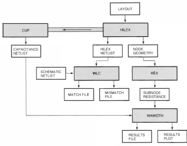
As the microarchitectural concepts solid ified . the design team realized that NVAX would be tbe largest and most complex chip ever designed at Digital, and that it wou ld place unprecedented stress on the capabilities of both designers and cJesign tool s. Accordingly, they initiated a partner ship with the Semiconducror Engineering CAD Group to improve current tools and to develop new tools. In addition to traditional areas l ike simu
la-10
tion,
CAD
development focused on improvements to productivity and accu racy through design syn thesis, electromigration analysis, and capacitance and resistance extraction.The size and complexity of the design, as well as the stringent schedule constraints, also d ictated an early start on verification issues. The verification strategy formed an i n tegral part of the design effort from the outset. The verification team developed tools and strategies for verifying the m icroarchitec ture, the microcode, the logic, the circuits, the chip as a component, and the chip in a system .
Lastly, the various system groups- data center systems, office systems, workstations- began designing systems to util ize the NVAX chip's capabil ities. Each group was able to b u i ld on the work clone in past VAX systems and designed an NVAX based system that functioned both as an u pgrade of past systems and as a formidably competitive new system in its own right.
The work of these project teams dovetailed per fectly. NVAX completed design and taped-out in late November 1990, just as the CMOS-4 process was ready for chip prototyping. Due to the outstanding work of the chip design , system design, CAD, and verification teams, first-pass parts booted the VMS operating system at speed in early March 1991. The process team qual ified CMOS-4 in October 1991, and systems using second-pass parts shipped tor rev enue t hat same month- three months ahead of schedule -with performance significantly greater than the original goaL
Clearly, the outstanding results from all the NVAX
The NVAX
and
NVAX
+
Highperfo
rma
nce
�AficrojJrocessors
G. Michael Uhler Debra Bernstein Larry L. Biro john E Brown III
john H. Edmondson jeffrey D. Pickholtz Rebecca L Stamm
The
NVAXand
NVAX +CPU chips are high-performance
VAXmicroprocessors that use
techniques traditionally associated with
RJSC
microprocessor designs to dramati
cally improve VA)( performance. The two chips provide an upgrade path for existing
VAX
systems and a migration path from VAX systems to the new Alpha AXP systems.
The design evolved throughout the project as time-to-market, performance, and
complexity trade-offs were made. Special design features address the issues of
debug, maintenance, and analysis.
The NVAX and NVAX+ CPUs are high-perform ance, si ngle-chip microprocessors that implement Digital's VA.'< arch itecture . 1 The I\fVA.'\ chip provides an upgrade path for existing systems that use the previous gener::ttion of VAX microprocessors. The NVAX+ ch ip is used in new systems that support Digital's DECchip 21064 m icroprocessor, which implements the Alpha AX P architecture 2-' These two NVA.'\ chips share a basic design.
The high-performance, complementary metal ox ide sem icond uctor (CMOS) process used to implement both chips allows the appl ication of pipeli ning techniques traditionally associ::tted with reduced i nstruction set computer (RISC) CPUs.·< Using these techn iques dramatical ly improves the performance of the NVAX a nd NVAX+ chips as com pared to previous VAX microprocessors and resu l ts in performance that approaches and may even exceed the performance of popular industry RJSC m icroprocessors.
The chip design evolved throughout the project as the goals influenced the schedule, performance, and complexity trade-offs that were made. The two primary design goals were t ime-to-market, without sacrificing qual ity, and im proved VA.'\ CPU performance. Our internal goal was for the NVAX CPU performance to be more than 25 times the performance of a VAX-1 1/780 system in a datacenter system. Achieving these goals required meeting aggressive schedules ancl thus concentrating
Digital Teclmical]ournal Vol. 4 No. 3 Summer 1992
on the high-leverage design points and on an unprecedented verification effort.'
Support for multiple system environments, compatibil ity with previous VAX products and systems, and a means to m igrate from t raditiona l VAX systems t o the new Alpha AXP platforms were also important design goals. These goals had a pro found impact on the design of the cache protocols and the external bus interfaces. NVA..'C and NVAX+ engineers worked closely with engineers i n Digital's systems groups during the definition of these operations.
The paper begins by comparing the basic fea tures of the NVA.'< and NVAX+ chips and then describes in detail the ch ip interfaces and design elements. This description serves as the fou ndation for the ensu ing discussion of design evol ution and trade-offs. The paper concl udes with information about the special design features that add ress the issues of debug, mai ntenance, and analysis.
Comparison of the NVAX
and NVAX + Chips
The NVAX and NVAX+ chips are identical in many respects, differing primarily in external cache and bus support. NVAX is intended tor systems that use previously designed VA.'C microprocessors. The following systems cu rrently use the NVA.'C chip: the VA..'\station 4000 Model 90; the MicroVAX 3100 Model 90; the VAX 4000 Models 100, 400,
NVA,'(-microprocessor VAX Systems
'iOO,
and ()()(); and the VAX()OOO
Model(}()() -"
-s ') NV.\X su pports an exte rnal wri te-back cache that i mplements a d i rectory-based b roadcast coherence protocol that is compatible with earl ier VAX systems. 1"NVAX+ is designed t< Jr system s that usc t h e DECchi p 2 10 6 4 m i c roprocessor i m plementation of the Alpha AX!' a rc h i tecture and is c urrently used in the VAX 7000 Mod el
(iOO
and the VAX 10000 Model (}OO S\ stems. NVAX+ su pports an external cache a mi bus protoco l t hat is compatible with that of the D!Tchip 2 1 0()4 m icroprocessor. In ex isting S\'stems. '\VAX+ is eonfigu reLI to su pport an exter nal write-back cache that i mplements a cond itional write-update snoopv cohere nce protoco l . 1 1The two Cl'l l chips prov ide both the means to upgrade i nstal led VAX S\'Stems, thus protecting pre vious investment s, and a m igra t ion path from a VAX m icroprocessor to a DECc h i p 2 1 0()4 m i c roproces sor in t he new Alpha AX!' systems.
Chip Inteifaces
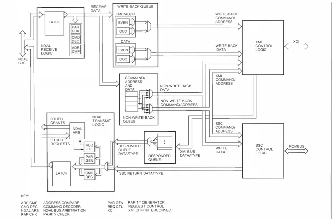
The NVAX chip i nterfaces to an external write-hack cache C H -eadle) through a p rivate port with tag and data static random-access memories ( RA.\ls) on t h e modu le, as shown in Figure I. The ize a nd speecl of the cache are program mable, a l lowing the c h i p to accom modate a range of possible sys tem config u rations.
The 1 AX data and add ress l i nes ( N DA L) con stitu te a 64-bit bid irectional external bus with asso ciated control signals that opera tes at one- t h i rd the frequency of the C:P l l from clocks prov ided by the C:l'll. Add resses and daL1 a re t ime- m u l t iplexed and,
OSC I LLATOR
NVAX
to provide high performance , a re overlapped with a rbitration for fu ture transactions and acknowl edgment of· p rev ious transactions. The N DAL bus protocol a l lows u p to t wo d isconnected reads and m u l t iple write-backs to be outstandi ng at tbe same time, using identifiers to d is tingu ish the d i fferen t t ransactions. External i n terrup t requests a re received t h rough ded icated l i nes and arbitrated by
logic in the C:l'l l.
The NVAX+ chip in terfaces to an external write- hack B -cache i m plemented w i th tag a mi data
static I�A Ms on the module t h rough a port shared with system con tro.l Iogie , as shown in Figure 2. Responsi b i l i ty for cont ro l l i ng the cache port is shared between NVAX+ and the system e nviron ment: the NVAX+ ch ip hand les the com mon cases of read h i t ami exclusive write. a mi the system environment prov ides cache policy control for o t her events. 'The size and speed of the cache can be configu red to al low a ra nge of possible system co nfigu rations.
The DE<:chip 21064 data and add ress l ines (EDAL) constitu te a dem u l t i plexed, bidirectio nal bus with 2<) bits of add ress. 1 28 b i ts of data, and the associ ated contro l signals. This bus opera tes at one- h alf, one-third , o r one-fo u rt h the frequency of the CPU from c locks prov ided lw the CPU. The speed of the system clocks can be program med to accom mo date various RAM and system speeds. At power-up time, i n i t i a l ization i nfo rmation, i ncluding RA�I rim ing, and d iagnostics are loaded from a serial read-only memory (RO�'I) into the on-chip cache. ·rhe external i n terrupt hand l i ng is similar to t hat of the NVAX chip.
C A C H E TAG
ADDRESS B-CAC H E
DATA TAG AND
DATA RAMS
NDAL
CONTROL SYSTEM
LOGIC
INTERRUPTS
SYSTEM CLOCKS
Ngm·e I NVAX ChifJ Interface Block
/)iagmm17Je NVAX and NVAX + HigiJ-petjonna nce
VAX
MicroprocessorsOSC I LLATOR CACHE TAG
SERIAL ROM ADDRESS B-CAC H E
DATA TAG AND
DATA RAMS
NVAX+
EDAL
CONTROL SYSTEM
LOG I C
I NTERRUPTS
[image:15.594.142.446.90.246.2]SYSTEM CLOCKS
Figure 2 JVVAX + Chip fn teJface Block Diagram
Electrical and Physical Design
Architectural Design
Process tech nology, clocking scheme, clock fre quency, and clie specifications are elements of the electrical and physical design of the NVAX and NVAX+ chips. Both chips are implemented i n Digital's fo urth-generation complementary metal oxide semiconductor (CviOS-4) technology. CMOS-4 is a 0.75-micrometer, 3.3-volt process with support for 5-volt input signals at the pins. The CMOS-4 process is optim ized for h igh-performa nce micro processors and provides short (05 -micrometer) channel lengths and three layers of metal i nter connect. This robust and reliable process has been used to produce NVAX chips in volume fo r more than a year and is the same CMOS process used in the DECchip 2 1064 m icroprocessor.
NVA)( and i\TVAX+ use a four-phase clocki ng scheme, d riven by an osci l lator that operates at four times the internal clock frequency. The oscil lator frequency is d iv ided by an on-chip, fin ite state-machine clock generator; a low-skew clock d istribution network is used for both internal and external clocks.
To meet the needs of the system designer, the two chips are designed for use at various frequen cies. At present, NVAX is used in systems at internal clock frequencies of 83.3 megahertz (MI-lz) (12-nanosecond [ns] clock cycles), 74.4 M l-lz (14-ns clock cycles), and 62.5 M Hz (16-ns clock cycles). NV�'{+ is used in systems at a frequency of 90.9 MHZ (11-ns clock cycles).
Each chip contains 1 . 3 m ill ion transistors on a die that is 16.2-by-14.6 millimeters in size. NVA)( is packaged in a 339-pin, through-hole pin grid array. NVAX+ is packaged i n a 431-pin, through-hole pin grid array.
Digital Technical journal 14>1. 4 No J Summer 1')')2
The NVAX/NV�"\+ design i s partitioned into five relatively au tonomous hmctional units: the instruc tion fetch and decode unit ( I-hox), the integer ancl logical instruction execution unit (E-box), the float i ng-point execution unit (F-box), the address trans lation and pri mary cache i nterface ( M-box), and the external cache ancl system bus interface (C-box). Queues placed at critical interface boundaries nor malize the rate at which the units process i nstruc tions. A block diagram of the NVAX and N VAX + core is shown in Figure 3.
The !-box
The 1-box fetches a nd decodes V�'{ instructions, eva luates operand specifiers, and queues operands in canonical form for further processing. incl uded in the 1-box is a 2-kilobyte
(KB),
direct-mapped vir tual instruction cache(VIC)
with 32-byte cache blocks. For reliabi lity, the VIC includes parity pro tection on both tags and data.-
- -
-- - - - -
--
--
-
, -1 I I I IE-60X, F-BOX
I
I
I
I
�
- - -
- -
- - -
- -
- -
- -
- -
- - -
- -
'
C-BOX
r
LATCH '---'Figure
3
Block Diagmm of theNVAX/NVAX
+ CoreM BOX
- - ,- - - Zoox
_ _ _- -
,I
I I
6-CACHEI
The NVAX and NVAX + Highperfnrmance VAX Micrnprncessors
queues, and the branch-related information into the branch queue.
For operand specifiers other than short l iteral or register mode, the 1-box decode logic invokes the pipel ined complex specifier unit (CSU) to compute the effective address and initiate the appropriate memory request to the M-box. The csu is similar in fu nction to the load/store unit on many traditional RISC machines.
The 1-box automatica l ly redirects the program counter (PC) to the target address when it decodes one of the fol lowing instruction types: uncon ditio nal bra nch, jump, and subroutine ca ll and return. The branch-taken penalty is two cycles for any conditional or unconditional branch. To keep the pipeline fu l l across conditional branches, the 1-box i ncludes a 512-bit by 4-bit branch prediction array. The pred iction is entered i n the branch queue by t he 1-box and compared with the actual branch direction by the E-box. If t he 1-box predicts incor rect ly, the E-box invokes a trap mechanism to d rain the pipeline and restart the 1-box at the alternate PC. A branch rnispredict incurs a four-cycle penalty fo r a branch that is actually taken and a six-cycle penalty for a branch that is not taken.
The E-box
The E-box is responsible for the execution of a l l non -floating-point instructions, for interrupt and exception hand ling, and for various overhead func tions. Al l fu nctions are microcode-control led, i.e. , driven by a microsequencer with a 1 ,600 -word con trol store and a 20 -word patch capability. Since the control store does not l imit the cycle time, we chose to implement a single microcode control scheme, rather than hard wire control for the simple instructions and provide microcode control for the remaining instructions.
The E -box begins instru ction execution based on information taken from the instru ction queue. References to specifier operands and resu lts are made indirectly through pointers in the source and destination queues. In this way, most E-box instruc tion flows do not need to know whether operands or resu lts are in register, memory, or instruction stream.
To i mprove the performance of certain critical instructi ons, the E-box contains special-purpose hardware. A mask processing unit fi nds the next bit set in a mask register and is used in the follow ing instructions: FFC. FFS, CALLS, CALLG, RET. PUSHR,
Digital Technical jountal Vol. 4 No. 3 Summer 1992
and POPR. A popu lation coun ter provides the num ber of bits set in a mask and is used in the CALLS, CALLG, PUSHR, and POPR instructions. In add ition, microcode can operate the arithmetic logic unit (ALU) ancl shifter independently to produce two computations per cycle, which can significantly i mp rove the parallel operation of the complex instructions.
In addition to normal instruction processing, the E -box performs aJ J power-up functions and inter rupt and exception processing, directs operands to the F-box , and accepts resu lts from the E-box. To guarantee that i nstructions complete in instruction stream order, the E-box orchestrates resu l t stores and instruction completion between the E-box and E-box .
The F-box
The F-box performs longword (32-bit) integer mul tiply and floating-point instruction execution. The E-box suppl ies operands, and the F-box transmits results and status back to the E-box .
The F-box contains a four-stage, floating-point and integer-mu lt iply pipel ine, and a nonpipe lined, floating-point divider. Subject to operand ava ilabi lity, the F-box can start a single-precision, floating-point operation during every cycle, and a double-precision , floating-point or integer-mu l tiply operation during every other cycle.
Stage 1 of the p ipeline calcu lates operand expo nent differen ce, adds the fraction fields, performs recoding of the mul.tipl ier, ancl compu tes three t imes the mu ltiplicand . Stage 2 performs al ign ment, fraction mu ltiplication, and zero and leadi ng one detection of the intermediate resu lts. Stage 3 performs normalization, fraction add ition, and a rniniround operation for floati ng-point add, sub t ract, and mult iply instructions. Stage 4 performs rounding, exception detection, and con dition code eva l uation.
Stage 3 performs a minirou nd operation on the resu l t calcu lated to that point to determine if a fu l l round operation is required i n Stage 4. To do this, a round operation is performed on only the low order three (for single-precision) or six (for double precision) fraction bits of the resu lt. If no carry-out
occurs fo r this operation, the remaining fraction bits are not affected and the fu l l stage 4 round oper ation is not req uired. If the fu l l round is not required, stage 4 is dynamically bypassed, resulting in an effective three-stage pi pel in e.
NVAX-microprocessot· VAX Systems
Tbe M-box
The M-box is responsible for address translation, access checki ng, and access to the primary instruc tion ancl data cache (P·cache). The M-box accepts requests from mu ltiple sou rces and processes these requests in an order that reflects both the pri ority of the request and the need to maintain instruction stream ordering of memory reads anc.l writes. Address translation and cache access are fu lly pipel inecl; the M-box can start a new request at the beginning of every cycle.
The M-box performs address translation and access checking by means of a 9o -entry, fu l ly asso cia tive translation buffer (TB) with parity p rotec tion. If a TB miss occurs, the M-box automat ica lly invokes a hardware miss sequence that calcu lates the address of the page table entry (PTE) that maps the page, fetches the PTE from memory, refil ls the TB, and restarts the reference. TB a l location is per formed using a not-last-used scheme, which is similar to a ro und-robin but guarantees that the most recently referenced entry will not be over written . The M-box reports access violations and page faults to the £-box, and £-box microcode pro cesses these misses with hardware support from the M-box.
The M-box also translates memory destination operand addresses provided by the !-box and saves the correspond ing physical add ress in the physical address (PA) queue. When the E-box stores a result, the M-box matches the data with the next address in the PA queue and converts this data to a normal write request. The PA queue is also used to check for confl icts in read requests to a location in which nothing has been written.
The P-cache is an 8KB, two-way set-associa tive cache with 32-byte blocks and parity protection on tags and data . The P-cache can be configured to cache instructions, data, or both, and usual ly bas the la tter configu ration. For compatibility with the DECchip 21064 microprocessor, the NVAX+ P-cache can also be configured into a direct mapped organization.
Tbe
NVAX
C-box
The NVAX C-box main tains the interface to the exte rnal B-cache and to the N DAL bus. The C-box receives read and write requests from the M-box and mon itors the NDAL for activity that wo uld requ ire an inval idate operation in either cache. Consecutive writes to the same quadword (o4 bits) are merged into a single quadword datum by
! 6
packing logic placed a t the input o f a n eight-entry quad word write queue.
The C-box can accept one instruction read request and one data read request from the M-box. Conflict logic in the write queue al lows noncon flicting read requests to be processed before queued write requests are performed . Conflicts are rt:solved by processing write queue entries u ntil the conflicting write is com pleted .
The C-box supports fou r B- cache sizes: 128KB. 256KB, 5l2Kfl, and 2 megabytes (MB). The system designer can independently select tag ancl clata RAJ\11 speeds to meet system requirements, regardless of the frequency at which the CPU is running. The B-cache block size is 32 bytes, and both tag and data RAMs are protected with error correction code ( ECC) that corrects single-bit errors and detects both double-bit errors ancl fu ll 4-bit RA.VI fail ures. The B-cache implements a directo ry-based broad cast coherence protocol in conjunction with a memory directory containing one bit per 32-byte block. Each memory directory bit ind icates if the associated block is valid in memory or has been written and exists in a cache. Unwrit ten blocks may exist in multiple caches in the sys tem . Written blocks may exist in exactly o ne cache.
An attempt to ""rite to a block that is not both val id and already written in the B-cache causes the C-box to request write permission from memory by means of a sp ecial NDAL bus read co mmand. The memory control ler will not respond to any NDAL bus transactions to a block that is writ ten in a cache. Instead, it waits for the CPU, which contains an updated copy of the block, to write the block back to memory and then com pletes the original transact ion . Al l CPUs in the system monitor the N DAL bus fo r read and write transactions and com pare the address against their B-cache tags. I f a match is found, the cache block is either writ ten back to memory, invalidated , or both, depend ing on the transaction type and the state of the block in the cache.
The N DAL protocol fu l ly supports mul tipro cessing implementations and uoes not requ ire any special chip variants to construct a mul tiprocessor system. The C-box invokes invalidate or write-back requests as requ ired to keep the B-cache and P-cache coherent with NDAL activity.
The
NVAX +
C-box
The NVAX+ C-box provides the interface between the internal fu nctional units and the EDAL pin bus
The NVAX and NVAX + Higbper:formance VAX Microprocessors
im plemented by the DECchip 21064 micropro cessor. This C-box i nterface inclu des the basic inte rface control for the external B-cache and for the memory and 1/0 system. The NVAX+ C-box receives read and write requests from the M-box. These requests are queued and arbitrated within the C-box and resu lt in cache or system access across the EDAL. The NVA)\+ C-box also maintains cache coherency by sending inval idate requests to the M-box when requested by external logic.
The NVA.'C+ C-box i mplementation provides many of the same features and performance enhancements available in the NVA.'\ C-box. Included is support for software-programmable B-cache speeds (one-hal f, one-third, or one-fourth times the CPU frequenq) and sizes (1 28KB to 8MB), write packing, write queu ing, and read-write reordering. In addition, the l\TVAX+ C-box supports the newer platforms and increases the degree to which NVA.X+ is compatible with the DECchip 21064 microprocessor. NVAX+ C-box features include program mable system clock speeds, I!O space-mapping, and a clirect-mapped option on the P-cache.
A major difference between the NVAX and NVAX+ implementations is in the B-cache coherence proto col. Rather than mandate a fixed B-cache coher ence protocol , the NVAX+ implementation al lows systems to tailor the protocol to their particu lar needs. 1\f\'A.'\+ cache coherency is implemented jointly by off-chip system support logic and by the CPU chip, with relevant information passed between the two over the EDAL bus. To al low dupli cate cache tag stores (if they exist) to be prope rly updated , the J\TVAX+ C-box provides i nformation to off-chip logic, ind icating when the internal caches are updated . Externa l l ogic notifies the N VA.'C+ C-box when an internal cache entry needs to be invalidated because of external bus activity.
Existing systems configure the B-cache to i mple ment a conditional write-update snoopy protocol carried out using shared and written signals on the system bus. Writes to shared blocks are broadcast to other caches for conditional update in those caches. A et>l.J that receives a write u pdate checks the J\TVA.'C+ P-cache to determine if the block is also present in that cache. If the block is present, the B-cache u pdate is accepted and written i nto the B-cache, and the P-cache is inval idated . If the data is not present in the P-cache, the B- cache is invali dated. This res ul ts in a write-update protocol for data that was recently referenced by a CPU (and hence is va I id in the P-cache) and reduces to a
Digital TeciJuical journal Vol. 4 No. 3 Summe·r 1')<)2
write-inva l idate protocol for data that was not recently referenced.
To accom modate the programmable nature of both the system and cache clock frequencies, the NVA.'<+ C-box supports nine different combinations of cache and system clock frequencies. This sup port allows efficient use of the chip in a wide range of different performance class systems.
Pipeline Operation
The NVAX. and NVAX+ chips implement a macro p ipel ine. M u ltiple VA.'\ macroinstructions are pro cessed in parallel by relatively autonomous fu nctional u nits with queued in terfaces at critical boundaries. Each fu nctional unit also has an inter nal pipel ine (micropipeline) to al low a new oper ation to start at the begi nning of every cycle. The pipeline operation can be logical ly depicted, as shown in Figure 4.
In pipeline segment SO, instruction stream data is read from the VIC. The next VAX instruction com ponent is parsed, and queue entries are made in segment S l . For short literal and register specifiers, no other processing is required. Requests for fm ther processing for a l l other specifiers are queued to the CSU pipel ine, which reads operand base addresses in segment 52, calculates an effective add ress, and makes any required M-box request contained in segment 53. If an M-box request is m ade, address translation and P-cacbe lookup occur in segments 54 and 55.
Instruction execu tion starts with a n E-box control store lookup in segment 52, followed by a register file read of any required operands in segment 53, an ALU and/or shifter operation in seg ment 54, and a potential result store or register file
write in segment 55. If an M-box request is required, e.g., for a memory store, the request is made in seg ment 54; add ress trans lation or PA queue access occurs in segment 5 5 ; and a P-cache access occurs in segment 56.
Floating-point and integer-mu l tiply instruction execution starts in the E-box, which transfers oper ands to the F-box. The four-stage F-box pipeline is skewed by half a cycle with respect to the E-box pipel ine, beginning halfway through segment 54. The fourth segment of the F-box pipeline is con di tiona l ly bypassed if a fu l l - round operation is not required . The result is transmitted back to the E-box, logically in segment 5 5 of the pipe line.
Pipeline bypasses exist for all important cases in the !-box and E-box pipelines, so that there are
NV AX-microprocessor VAX Systems
I NSTRUCTION FETCH, DECODE, SPEC I F I E R EVAL, MEMORY REQU EST
I NTEGER, LOGICAL INSTRUCTION EX ECUTION
FLOATI N G-POINT INSTRUCTION EXECUTION
KEY
s SEGMENT
so
SPECI F I E R EVAL INSTN
OPERND MEMREQ
SPECIFIER EVALUATION INSTRUCTION
OPERAND
TB
MEMORY REQUEST TRANSLATION BUFFER
S 1 S2
ALU cs
S3
EXPON DIFF ALIGN, FRMUL T NORM, FRADD BYPASS ROUND
S4 S5 S6
ARITHMETIC LOGIC UNIT CONTROL STORE EXPONENT DIFFERENCE
S7 S8
BYPASS I ROUND 1
ALIGN MENT A N D FRACTION M U LTIPLY NORMALIZATION AND FRACTION ADDITION RESULT ROU N D I N G AND BYPASS
Figure 4 Pipeline Organization
no sta ll s for results feed ing d i rectly into su bse quent operands. The M-box processing of memory references initiated :�s a result of operand speci fier processing by the !-box is usua l ly overlapped with the execution of the previous in struction in the E-box, with few or no stal ls occurring on P-cache hit.
Design Evolution and Trade-offs
The NV�"X and NVAX+ chips are the latest in a l i ne of GviOS VAX microprocessors designed by D igit a l "s
engineers and represen t a continuing evolution of architectural concepts from one implementation to the next. The p reced i ng chip design was the CPU for the VA}( 6000 Model 400 system. 11 To meet the time-to-market and performance goals, we had to modify the NVAX/NVAX+ design throughout the project.
One of the early vehicles for making design tracle-offs was the NVA.X perform ance model, which predicts CPU and system performance and a ids in quantifying the performance impact of va rious design option s. The performance mode.l is a detailed , trace-d riven model which can be easily configured by changing any of a variety of input parameters. The model stim u l i used were 15 generic timesharing and 22 bench mark instruction trace files that were captured by running actual programs on existing VAX systems.
The fo l l owing sections describe the evo lution of the chip design, including the nu mber of chips, the p ipel ining tech nique used, and various cache issues.
1 8
Number of CPU Chips
The VAX 6000 Model 400 core CPU imp lementation i s a three-chip design: a processor chip, with a smal l on-chip primary cache; a fl oating-point chi p ; a n d a secondary cache control ler. with in ternal cache tags. The i n itial attempt at N"V�"X CPll defini tion was a two-chip design. One chip contai ned the 1-box (with a 4KB
VlC). tbe E-hox. the F-box, and
the M-box (with a I6KB , direct-mapped P-cache) The second chip held the C-box and the B-cache tag a rray. The project design goa ls, especia!Jy t ime-to ma rket, Jed to a s ingle-chip solution. rather than a two-chi p design.To condense the design f rom two chips to one, we halved the s izes of the VlC and the P-cache and moved the B-cacl1e tags to external static RAMs, leaving the B-cache con trol ler on-chip. Later, we were able to reduce the penalty of halving the size of the P-cache by making it two-way set associative rather than direct mapped. W ith these changes, the perfo rmance model showed a performance loss of less than 1 .4 p e rcen t across al l the traces, relat ive to the two-chip design, with a worst-case penalty of 3.9 percent.
There are strong advantages to the s ingle-chip sol u tion .
• Designing a single chip takes less t i me.
• This design requ ires the prod uction ami main tenance of only one design database and one mask set.
• Latency to the B-cache is shorter.
• An off-chip tag store provides more f lexibility i n B-cache conf igurations.
T he NVAX and NVAX + High-performance VAX Microprocessors
Macropipelining
Run -time performance is the product of the cycle time, the average time to execute an instruction (cycles per instruction [CPI]) and the number of instructions executed. CMOS process improve ments made it possible to decrease the NVAX/ NVAX+ cycle time with respect to the previous gen eration of VAX microprocessors, thus improving the first factor in run-time performance.
The VJL'( 6000 Model 400 CPU design uses tra d itional microinstruction pipelining, i.e., micro pipelining, to achieve some amount of overlap and to decrease the CPl. However, using m icropipe lin ing techniques would not reduce the NVJL'(/ NVJL'\+ CPI to the level required to meet the perfor mance goals of the NVJL'(/NVJL'\+ projects. We achieved this reduction by using ruse design and implementation techniques referred to as macro pipelining. In a macropipelined architecture, the 1-box acts much like a load/store engine, dynam ically prefetching operands prior to instruction execution. Using the macropipeline technique in the NVAX and NV�L'\+ crus makes it possible to retire one basic complex instruction set computer (CISC) macroinstruction per cycle, as in a simple RISC design. Although m acropipelining introduced considerable com plexity into the NVAX/NVAX+ design, this complexity resulted in a significant performance improvement over a traditional micropipelinecl design.
Number of Specifiers per Cycle
The NVAX/NVAX+ 1-box can parse at most one opcocle and one VAX specifier per cycle. The 1-box design initiaHy considered was capable of parsing two specifiers per cycle. Although this parsing scheme represented significant complexity and cir cuit risk, intuitively, it seemed important to quickly retire specifiers in the 1 -box in order to keep the macropipeline full. However, the performance model predicted a maximum performance improve ment of less than two percent on our traces, and we decided to limit complexity and schedule risk by parsing only one specifier per cycle.
F-box Design
The 1\TVAX F-box design is highly leveraged from the VAX 6000 Model 400 F-chip design. Rather than start from scratch, we integrated the existing design onto the 1\TVAX and NVAX+ CPU chips and added a final -stage bypass mechanism. In add ition,
D igital Tee/mica/ journal \I(J/. 4 No. 3 Summer 1992
unlike the original F-chip implementation, the NVAX/NVAX+ control of the F-box allows a fully pipelined operation, which significantly improves floating-point performance over the F -chip design. Although a totally new design would have had shorter floating-point latencies, the combination of a fu lly pipelined operation and a final-stage bypass allowed us to achieve our perfo rmance goal, while meeting our time-to-market goal.
Cache Coherence
Performance studies with the previous generation of VAX microprocessors clearly indicate that system bus write bandwidth .limits performance unless an external write -back cache is implemented. In addi tion, the VAX architectme required that we imple ment the cache coherence protocol in hardware. The NV!L'\ implementation uses a directory-based coherence protocol for compatibility with existing and planned target system platforms. The NDAL bus supports mu ltiple outstanding read and write requests, which allows the microprocessor to uti lize the capability of the system bus to process these operations in a pipelinecl fashion. We investi gated the possibility of implementing both direc tory-based ancl snoopy coherence protocols, but time-to -market considerations and the opportunity to optimize the design for performance in existing system platforms outweighed the desirability of supporting snoopy protocols.
For the 1\TVAX+ implementation, the coherence policy is determined by hardware external to the
NVAX+ chip, in the given system. The 1\TVAX+ cache and system interface allows the system environ ment to implement a variety of coherence pro wcols Compatibility with the DECchip 21064 interface definition required limiting 1\TV!L'\+ to one outstanding external cache miss. However, this limitation is more than offset by the significantly better main memory access times achieved in target systems.
One significant advantage of the l\TVAX+ scheme is that most policies associated with the external cache are determined by hardware outside the NVAX+ chip (such as the coherence policy), allow ing the chip to be used in a wide variety of systems. Implementing the DECchip 21064 interface on NV!L'\+ greatly reduces the hardware engineering investment required to deliver a VAX CPU and an
Alpha AXP CPU in the same system environment. For both the NVJL'( and the l\TVAX+ chips, cache coherence is maintained for the P-cache by keeping