FPGA Implementation of Interrupt Controller (8259) by
using Verilog HDL
L. Padma Sree, PhD.
Professor
Department of ECE,VNR VJIET
Hyderabad, India
Bekkam Satheesh
M.Tech, VLSI
Department of ECE,VNR VJIET
Hyderabad, India
N. Dhanalakshmi
Associate Professor
Department of ECE,VNR VJIET
Hyderabad, India
ABSTRACT
A Priority Interrupt Controller is a hardware designed chip which acts as an overall system manager to efficiently handle the multiple interrupts that tend to occur from the varied number of peripheral devices. Hence, it relieves the system‟s CPU from the task of polling in a multilevel priority system. This paper deals with implementation of a Priority Interrupt Controller using Verilog language. During the implementation, the Verilog code has been written for all the internal registers of the Priority Interrupt Controller so that it can accomplish its task of prioritizing the various interrupts and thereby increasing the efficiency of the processor. In this paper the entire functional block was sub divided into various modules like vector address module, command register module, mask register module and finally it was integrated into a single unit to accomplish specified tasks. In the present work the Priority Interrupt Controller was made to operate in three different modes-Fully Nested Mode, Rotating Priority Mode, and Special Mask Mode.
Keywords
FPGA, Fully Nested Mode, Interrupt Controller, Rotating Priority Mode, Special Mask Mode.
1.
INTRODUCTION
The Programmable Interrupt Controller functions as an overall manager in an Interrupt-Driven system. It accept requests from the peripheral equipment, determines which of the incoming requests is of the highest priority, ascertains whether the incoming request has a higher priority value than the level currently being serviced, and issues an interrupt to the CPU based on this determination. Each peripheral device or structure usually has a special program or “routine” that is associated with its specific functional or operational requirements; this is referred to as a “service routine”. The Priority Interrupt Controller, after issuing an interrupt to the CPU, must some how input information into the CPU that can “point” the Program Counter to the service routine associated with the requesting device. This “pointer” is an address in a vectoring table and is referred to as vectoring data.
This Priority Interrupt Controller is a device specifically designed for use in real time, interrupt driven microcomputer systems. It manages eight levels of requests and has built-in features for expandability to other 82C59As that is up to 64 levels. It is programmed by system software as an I/O peripheral. A selection of priority modes is available to the programmer so that the manner in which the requests are processed by the Priority Interrupt Controller (82C59A) can be configured to match system requirements. The priority modes can be changed or reconfigured dynamically at any time during main program operation.
2.
IMPLEMENTATION
The Priority Interrupt Controller 82C59A is divided into various modules like Vector Address Module, Mask Register Sub module, Mask Register Module, Command Register Module, Interrupt Modes Module. All the codes of the modules are integrated using a Top Module and waveforms for various modes - Fully Nested Mode, Rotating Priority Mode, and Special Mask Mode have been obtained.
The powerful features of the 82C59A in a microcomputer system are its programmability and the interrupt routine addressing capability. The latter allows direct or indirect jumping to the specified interrupt routine requested without any polling of the interrupting devices. The normal sequence of events during an interrupt depends on the type of CPU being used.
2.1
Top Module
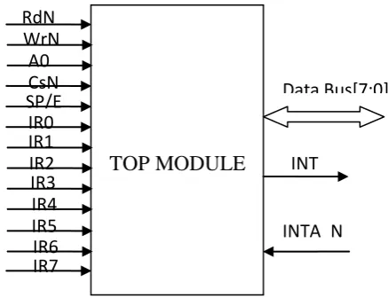
[image:1.595.327.546.436.604.2]The Fig 1: shows the top module of The Priority Interrupt Controller 82C59A.
Fig 1: Block diagram of Priority Interrupt Controller (82C59A)
2.1.1
Signal Description of Priority Interrupt
Controller (82C59A)
The table 1: shows the input/output control signals and their descriptions of Priority Interrupt Controller (82C59A).
TOP MODULE
RdN
WrN
A0
CsN
SP/E
N
IR0
Table 1: Signal description of Priority Interrupt Controller (82C59A)
S.No Signal Mode Description
1 CsN Input
This is also an active low signal, which controls the enabling and disabling of
the 82C59A.
2 RdN Input
A low on this signal enables the 82C59A to send the status of the IRR,
IMR, ISR and Interrupt Level
3 WrN Input
A low on this signal enables the CPU to write
control words to the 82C59A
4 A0 Input
This is used in conjunction with WrN and RdN signals to write commands into the
various command registers, as well as various
status registers of the 82C59A 5 SP/EN Input
6 IR0 Input
These seven signals are the Interrupt Requests from
the seven devices connected
7 IR1 Input
8 IR2 Input
9 IR3 Input
10 IR4 Input
11 IR5 Input
12 IR6
Input
13 IR7 Input
14 DataBus
[7:0] InOut
Control, Status, Interrupt Vector information is transferred through this
bi-directional bus. 15 INT Input This is the Interrupt signal
to the CPU
16 INTA_N Output
This is an Acknowledgement signal for the Interrupt Request to
the CPU by 82C59A.
2.2 Vector Address Module
2.2.1 Module Description
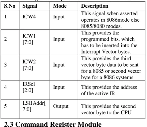
From the fig 2: The main purpose of this module is to generate the second Interrupt Vector Byte or the LSB Address to provide to the CPU. The IRSel signal provides the Interrupt Request, which is finalized after the priority, is resolved. The ICW4 signal decides whether the system is 8086 or the 8085 operated. During the second INTA# pulse sequence, the LSB Address is placed on the Data Bus to the CPU. For a MCS-8085/8080 system, there will be two bytes (LSB and MSB Addresses) to be passed, but for an 8086 operated system, only one byte cascades the code byte, which is the “CDH” for 82C59A.
Fig 2: Block Diagram of Vector Address Module
2.2.2 Signal Description of
Vector Address Module
[image:2.595.320.548.81.209.2]The table 2: shows the input/output control signals and their descriptions of Vector Address Module.
Table 2: Signal description of Vector Address Module S.No Signal Mode Description
1 ICW4 Input This signal when asserted operates in 8086mode else 8085/8080 modes.
2 ICW1
[7:0] Input
This provides the programmed bits, which has to be inserted into the Interrupt Vector bytes.
3 ICW2
[7:0] Input
This provides the third vector byte data to be sent for a 8085 or second vector byte for a 8086 systems
4 IRSel
[2:0] Input This provides the address of the active IR
5 LSBAddr[
7:0] Output This provides the second vector byte to the CPU
2.3 Command Register Module
2.3.1 Module Description
From the fig 3: The functionality of this module can be split into three parts .
writing the Command Words into the 82C59A.
Reading the Status of the Interrupt Mask Register (IMR), Interrupt Request Register (IRR), In-Service Register (ISR). Interrupt Response Mode.
Initially under reset (Rst=‟0‟), the module is initialized and when CsN signal is activated, the actual functioning of the module comes into picture. After this the „A0‟ is checked to be zero and the fourth bit of the data input is compared to be „1‟ and the ICW‟s are loaded into the 82C59A with active „WrN‟ signal. In the second part when „RdN‟ signal is activated, the status of the device is read by the CPU or the information of the Interrupt Mask Register (IMR), Interrupt Request Register (IRR), In-Service Register (ISR) are placed on the DataBus. In the Interrupt Response Mode, the whenever there is Interrupt Acknowledge (INTA_N) from the CPU, the Interrupt Vector bytes are placed on the “DataBus” by the 82C59A.
[image:2.595.309.550.301.509.2]Fig 3: Block Diagram of Command Register Module
2.3.2 Signal Description of Command Register
Module
[image:3.595.60.270.77.236.2]The table 3: shows the input/output control signals and their descriptions of Command Register Module.
Table 3: Signal description of Command Register Module S.No Signal Mode Description
1 Rst Input
This is an active low signal which is used for
initializing the Device 82C59A.
2 CsN Input
This is also an active low signal, which controls the enabling and disabling of
the 82C59A.
3 WrN Input
A low on this signal enables the CPU to write
control words to the 82C59A
4 RdN Input
A low on this signal enables the 82C59A to send the status of the IRR,
IMR, ISR and Interrupt Level
5 A0 Input
This is used in conjunction with WrN and
RdN signals to write commands into the
various command registers, as well as various status registers of
the 82C59A.
6 INTA_N Input
This signal is used to enable 82C59A
interrupt-vector data onto the data bus by a sequence of interrupt acknowledge pulses issued by the CPU
7 DataBus [7:0] Input
Control, Status, Interrupt Vector information is transferred through this
bi-directional bus.
8 LSBAddr[7:0] Input
This provides the second vector byte to be transferred to the CPU.
9 ICW1-ICW4 Output
These four outputs provide the Initialization
command words, which are written into the
82C59A.
10 OCW1 to OCW3 Output
These three outputs provide the Operation command words, which
are written into the 82C59A.
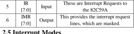
2.4 Mask Register Module
2.4.1 Module Description
From the fig 4: The functionality of this module can be fragmented into two parts. The first part involves the generation of Interrupt Request depending on the triggering mode used and the latter part is dedicated in masking the IR if required or else enabling. The Rst and the MClr signals are engaged in the initialization of the modules when asserted low.The first part can be further subdivided into two modes depending on the LTIM signal.Edge Triggered Mode if LTIM=‟0‟,Level Triggered Mode if LTIM=‟1‟.The second part of masking the Interrupt Request is dependent on the OCW1.The IR‟s whose corresponding bits in the OCW1 are high are masked else enabled.
Fig 4: Block Diagram of Vector Address Module
2.4.2 Signal Description
The table 4: shows the input/output control signals and their descriptions of Vector Address Module.
Table 4: Signal description for Vector Address Module S.No Signal Mode Description
1 Rst Input
This is an active low signal which is used for initializing the Device
82C59A.
2 MClr Input This is also an active low signal obtained from the
3 LTIM Input
When asserted the device operates in Level Triggered mode else
Edge Triggered mode.
4 OCW1 Input
This signal dictates whether the corresponding Interrupts has to be
masked or enabled.
MASK REGISTER
MODULE
Rst
MClr
LTIM
OCW1
IR[7:0]
IMR[7:0]
COMMAND
REGISTER
MODULE
Rst
CsN
RdN
Wr
N
A0
INTA_
N
DataBus[7:
0] IMR[7:0]
[image:3.595.47.290.342.725.2] [image:3.595.333.556.399.528.2]5 IR
[7:0] Input
These are Interrupt Requests to the 82C59A
6 IMR
[7:0] Output
This provides the interrupt request lines, which are masked.
2.5 Interrupt Modes
There are 4 modes of operation of 82C59A.
2.5.1 Fully Nested Mode
This mode is entered after initialization unless another mode is programmed. The interrupt requests are ordered in priority from 0 to 7. When an interrupt is acknowledged the highest priority request is determined and its vector places on the bus. Additionally a bit of ISR is set. This bit remains set until the microprocessor issues an End of Command (EOI) immediately before returning from the service routine or if the AEOI command bit is set, until the trailing edge of the last INTA#.
2.5.2 Automatic End Of Interupt (Aeoi)
If AEOI=1 in ICW4, then the 82C59A will operate in the AEOI mode continuously until reprogrammed by the ICW4.In this mode it will automatically perform a non-specific EOI operation at the trailing edge of the last interrupt acknowledge pulse. This mode is only used in a master 82C59A and not a slave.
2.5.3 Automatic Rotation
This mode provides all the interrupt devices with equal priority. In this mode a device, after being serviced, receives the lowest priority and the remaining devices are provided a n opportunity thus making the device which had been already serviced to wait in the worst case until each of the seven other devices are serviced.
2.5.4 Special Mask Mode
This mode finds its necessity when the system priority structure during its execution under software control. That is if an Interrupt Request is acknowledged and the End Of Interrupt (EOI) did not reset its ISR bit, the 82C59A would have inhibited all lower priority requests. In Special Mask Mode, when a mask bit is set in OCW1, it inhibits further interrupts from all other levels that are not masked. The Special Mask Mode is set by OCW3 where the SSMM=‟1‟ and SMM=‟1‟ and cleared when SSMM=‟1‟ and SMM=‟0‟.
2.5.5 Poll Command Mode
This mode is operated by masking or disabling the interrupts or by not connecting the INT output. The Poll Command is issued by setting P=‟1‟ in OCW3. The next RD# pulse is treated as an Interrupt Acknowledge, sets the appropriate IS bit if there is a request , and reads the priority level. This mode is useful if there is a requirement to expand the number of priority levels to more than 64 or when there is no requirement of INTA_N sequence.
3 RESULTS AND WAVEFORMS
The waveforms for the individual modules and for the different modes are shown:
[image:4.595.50.286.72.133.2]3.1 Vector Address module output
Fig 5: Output Waveform for Vector Address module
[image:4.595.316.566.72.261.2]3.2 Mask Register Sub Module
output
Fig 6: Output Waveform for Mask Register Sub Module
3.3 Mask Register Module output
[image:4.595.314.557.492.691.2]3.4 Command Register Module output
Fig 8: Output Waveform for Command Register Module
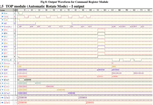
2.5
TOP module (Automatic Rotate Mode) – I output
[image:5.595.58.551.382.720.2]3.6 TOP MODULE (Automatic Rotate Mode) – II output
Fig 10: Output Waveform for TOP MODULE (Automatic Rotate Mode) – II
3.7 TOP MODULE (Specific Rotation Mode) –I output
3.8 TOP MODULE (Specific Rotation Mode) –II output
Fig 11: Output Waveform for TOP MODULE (Specific Rotation Mode) -II
3.9 TOP MODULE (Fully Nested Mode) – I output
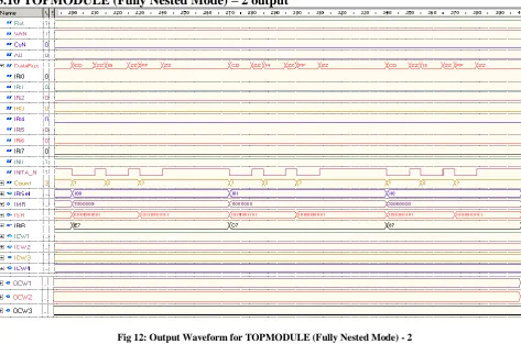
3.10 TOPMODULE (Fully Nested Mode) – 2 output
Fig 12: Output Waveform for TOPMODULE (Fully Nested Mode) - 2
3.11 FPGA implementation of the priority interrupt Controller 82C59A.
Fig 12: Output Waveform for FPGA implementation of the priority interrupt Controller 82C59A
4. CONCLUSION
This Priority Interrupt Controller is a device specifically designed for use in real time, interrupt driven microcomputer systems. It manages eight levels of requests and has built-in features for expandability to other 82C59As that is up to 64 levels. This Priority Interrupt Controller is implemented by using SPATRAN-3 Xilinx FPGA. From the results, the performance of the respective logics was verified with the assumptions that were taken into account when creating the logic. Hence, this work has been demonstrated the principles for designing a Priority Interrupt Controller-82C59A to meet the worst-case timing specifications
5. REFERENCES
[1]. William Stallings, “Computer Organization”, 7th Edition, Free Press, 2002.
[2]. Brown, Ralf/Kyle and Jim Paperback, PC Interrupts – 8259, 2nd edition, Addison-Wesley, 2006.
[3]. Joe McGovern, Interrupt – Driven PC System Design, 4th edition, Prentice Hall of India, 2003.
[4].Charles H. Roth, “Digital Systems Design”, 4th edition, Jr. PWS Publishing House, 1998.
[5]. Douglas J Smith, ”HDL Chip Design”, Doone Publications ,3rd Edition,1996.
[6]. Samir Palnithkar “Verilog HDL”, Prentice Hall PTR Publishers, 2nd edition, 2003.
[7].Donald E Thamas, ”The Verilog hardware description language”, Kluwer Academic publishers,5th
Edition, 2002.