Programmable Serial Interface
(PSI)
Hardware Reference Manual
FliD'J
HEWLETT.:a.
PACKARDThe Printing History below identifies the Edition of this Manual and any Updates that are included. Periodically, update packages are distributed which contain replacement pages to be merged into the manual, including an updated copy of this Printing History page. Also, the update may contain write-in instructions.
Each reprinting of this manual will incorporate all past updates; however, no new information will be added. Thus, the reprinted copy will be identical in content to prior printings of the same edition with the user-inserted update information. New editions of this manual will contain new information, as well as updates.
First Edition... June 1983 Update 1 .. ... ... ... .... ... ... ... December 1984
NOTICE
The information contained in this document is subject to change without notice.
HEWLETT-PACKARD MAKES NO WARRANTY OF ANY KIND WITH REGARD TO THIS MATERIAL, INCLUDING, BUT NOT LIMITED TO, THE IMPLIED WARRANTIES OF MERCHANTABILITY AND FITNESS FOR A PARTICULAR PURPOSE. Hewlett-Packard shall not be liable for errors contained herein or for incidental or consequential damages in connection with the furnishing, performance or use of this material.
Section GENERAL
I
INFORMATION
Physical Description •••••••.•••• ~ ••••••
Functional Description ••.•••••••••••• ". Identification .•••.•••••••••••.•••••
The Produc t •..•..•.••.
Printed Circuit Card ••.•••••••••••.•. Manuals ... .
Specifications •.
Section II INSTALLATION
Determining Current Requirements .. Firmware Installation ..
Switches and Jumpers... . .•••••.
Swi tches ...••.•..•....•...••••.. Memory Configuration Jumpers ....
Additional Jumpers ....•.
liD
Channel Interface ..••••.Peripheral Device RS-232-C Cable. RS-449 Cable ...
Interface .••••..
Direct Connect Installing the Checkout .... Reshipment ..
Section III
Cable. PSI ....
PRINCIPLES OF OPERATION
Functional Description ...•.... System Clocks ...•.•..••. Memory Address Space.
lID
Address Space ....Serial
lID
Controller ..••SID Registers ...•..••••.••.••
SID Modem Control and Status Bits •. PSI Card Modes of Operation ..•••.•
Control Lines .•...••. Operational Mode Definitions .. Self-Test Mode Definitions ..•.
CONTENT,S:
Page
• • • • • • a., • • • • • • • • • • • •
.
... .
1-1 1-1 1-3 1-3 1-3 1-6 1-6• • • • • • • • 'a • • • • • • • • • • • ,.
Memory Interface Ci rcui t (MI C) ••••••••••••••••••••.•••••.••••• 3-26
MIC Register 0 - Configuration •••••••••
~••••••••••••.•.•••.• 3-28
MIC Regi5ter 1 - Channel B High Memory Addres5 ••••••••••••.. 3-28
MIC Register 2 - Channel·B Low Memory Addres5 .••••••••..•... 3-29
MIC Register 3 - Channel B Configuration ••••••.•••.•••••.••• 3-29
MIC Register 4 - Channel B Low Byte Count .•••.•••.••.•.••... 3-29
MIC Register 5 - Channel B Port Address .•••••..••••••..•..•• 3-30
MIC Register
6 -Channel A High Memory Address ••••••.•.••..• 3-30
MIC Register 7 - Channel A Low Memory Addre5s ..••••..•...••. 3-30
MIC Register
8 -Channel A Configuration ••••..•.••..•..•.... 3-31
MIC Register 9 - Channel A Low Byte Count ••••••••.••.••..•.. 3-31
MIC Register A - Channel A Port Address •••••••••.•...•.•••.. 3-31
MIC Register B - Interrupt Vector ••.•••..••••...•.. 3-32
Priori ty Interrupt Structure •••••••••..•••••.••...••.••... 3-32
Section IV
Page
MA
I HTEtiAtiCE. • • '. • • • • • • • • • • • • • • • • • • • • • • • • • • • • • • • • • • • • • • • • • • • • • • • • • • • • 4-1Section V
REPLACEABLE PARTS
Page
Replaceable Parts ...•••.••.•.•...•...•...•..•••••...••••....•.••... 5-1
Ordering Information ...••...•..•.•... 5-1
Section VI
Page
SCHEMAT I C
DI
AGRAMS ••••••••••••••••••••••••••••••••••••••••••••••••• 6-1AppendiX A
Page
GENERAL INFORMATION
IF!~iHi,
This manual provides general information, installation procedures, theory of operation, maintenance
instructions, replaceable parts information, and servicing diagrams for the Hewlett-Packard
Programmable Serial Interface (PSI) Card. This section contains general information concerning the PSI, and includes a description and specifications.
PHYSICAL DESCRIPTION
The Programmable Serial Interface (PSI) card is shown in figure 1-1. One SO-pin connector con-nects the card to an Input/Output Adapter and from there to a host computer, and a 50-pin connec-tor connects the card to
a
peripheral device.The PSI card can be used in several applications, depending on the firmware ROM/EPROM installed on the card. The ROM firmware is explained in separate manuals, depending on the application. Thus, a product of which the PSI is a part will consist of:
The PSI Printed Circuit Assembly (also referred to as a card in this manual), part number 5061-4920.
One or two ROMs or EPROMS, or one ROM/EPROM and one static RAM.
Up to eight jumper plugs (mounted on the card) depending on the ROM/EPROM/RAM conf igura tion.
A cable, depending on the application.
This manual, part number 27132-90005.
An installation manual for the complete product (the part number will depend on the product).
A firmware manual (the part number will depend on the product).
PSI
Figure 1-2 shows a Hewlett-Packard computer system using CHANNEL I/O and the PSI.
(CHANNEL I/O is a Hewlett-Packard standard defining the physical and electrical characteristics for an I/O system consisting of an I/O channel, an I/O channel adapter, and I/O cards. The PSI is one of the I/O cards.)
Note that the computer system CPU and memory communicate directly along a Memory/Processor Bus (MPB). I/O data to/from peripheral devices reaches the CPU/memory through the I/O channel, the I/O channel adapter, and an I/O card such as the PSI card. The I/O data is received from and transmitted to peripheral devices by the I/O card, which converts device-specific data to a for-mat compatible with the I/O channel, and thus the computer. The I/O channel adapter (see figure
1- 2) controls the flow of traffic between the I/O channel and the memory/processor bus.
The PSI uses several of the Z-80 family of microprocessor components to relieve the host computer of much of the overhead.
IDENTIFICA TION
The Product
Up to five digits and a letter (27122A, for example) are used to identify Hewlett-Packard products. The five digits identify the product; the letter indicates the revision level of the product. Note that the PSI card is not a product by itself, it is merely one part of an interface product (other parts of the product are the manuals, ROMs or EPROMs, interface cables, etc.). The complete product is described in the firmware manual.
Printed Circuit Card
The printed circuit card is identified by an assembly part number marked on the card. In addition to the part number, the card is further identified by a letter and a four-digit date code (e.g., B- 2314). This designation is placed below the part number. The letter identifies the version of the etched cir-cuit on the card. The date code (the four digits following the letter) identifies the electrical characteristics of the card with components mounted. Thus, the complete part number on the PSI card is:
5061-4920 B-2314
If the date code stamped on the card does not agree with the date code on the title page of this
manual, there are differences between your card and the card described herein. These
MEMORY
1/0 CHANNEL ADAPTER
110
CARD
MEMORY
MEMORY/PROCESSOR BUS
1,0 CHANNEL
PSI
Manuals
This manual, part number 27132-90005, covers the PSI card (part number 5061-4920) only, without any ROMs/EPROMs installed. The PSI card in its complete form with ROMs/EPROMs, cables, etc., is covered in a firmware manual which describes the complete product. (Note that this manual and the
firmware manual are part of the HP 27132 Technical Reference Package.) A third manual, an
instal-lation manual, is shipped with the complete product and contains information on installing the product in the host computer.
The name, part number, and pUblication date are printed on the title page of each manual. If the
manual is revised, the publication date is changed.
SPECIFICA TIONS
Table I-I lists the specifications of the PSI.
Table I-I. Specifications
FEATURES
• One primary full-duplex 5ynchronou5/a5ynchronou5 5erial
lID
port• One 5econdary full-duplex a5ynchronou5 5erial
lID
port• A5ynchronou5 baud rate5 from 50 baud to 115'.2K baud
5, 6, 7, or 8 bit5/character
1, 1.5, or 2 5tOP bit5
Even, odd, or no parity
X1, X16, X32, or X64 clock mode5
Break generation and detection
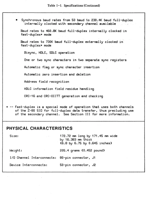
Table 1-1. Specifications (Continued)
• Synchronous baud rates from 50 baud to 230.4K baud full-duplex
internally clocked with secondary c::hannelayailable
Baud rates to 460.8K baud full-duplex internally clocked in fast-duplex* mode
Baud rates to 730K baud full-duplex externally clocked in fast-duplex* mode
Bisync, HDLC, SDLC operation
One or tw~ sync characters in two separate sync registers
Automatic flag or sync character insertion
Automatic zero insertion and deletion
Address field recognition
HDLC information field residue handling
CRC-16 and CRC-CCITT generation and checking
* -- Fast-duplex is a special mode of operation that uses both channels
of the
Z-SO
SID for full-duplex data transfer, thus precluding useof the secondary channel. See Section III for more information.
PHYSICAL CHARACTERISTICS
Size: 172.72 mm long by 171.45 mm wide
by 16.383 mm thick
(6.S by 6.75 by 0.645 inches)
Weight: 205.4 grams (0.452 pound)
lID
Channel Interconnects: 80-pin connector, J1 [image:10.613.71.555.68.747.2]PSI
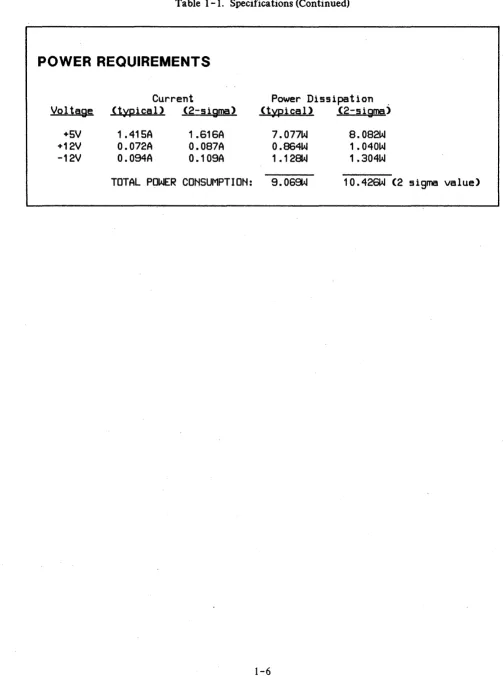
Table 1-1. Specifications (Continued)
POWER REQUIREMENTS
Current
Voltase (typical) (2-sisma)
+5V +12V
-12V
1 .415A
O.072A
O.OS4A
1.616A
O.087A
O.10SA
Power Dissipatlon .
(typical) (2-sigma)
7.077W
O.864W
1.128W
8.082W
1.040W
1 .304W
[image:11.613.50.554.84.768.2]INSTALLATION
1-~---~[[]
This section provides information on installing and checking the operation of the PSI.
DETERMINING CURRENT REQUIREMENTS
The PSI circuit card obtains its operating voltages from the host computer power supply through the I/O channel. Before installing the card, it is necessary to determine whether the added current will overload the power supply. The current requirements of the card are listed in the power require-ments entry of table 1-1 in Section I. Current requirerequire-ments for all other I/O cards can be found in the appropriate Technical Reference Manuals.
FIRMWARE INST ALLA TION
I
CAUTIONI
SOME OF THE COMPONENTS USED IN THIS PRODUCT ARE SUSCEPTIBLE TO DAMAGE BY ST A TIC DISCHARGE. REFER TO THE SAFETY
CONSIDERATIONS INFORMATION AT THE
FRONT OF THIS MANUAL BEFORE HANDLING THE CARD OR REMOVING OR REPLACING COMPONENTS.
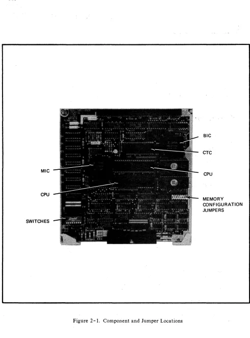
The EPROMs are installed in the sockets shown in figure 2-1. The types of ROMs/EPROMs that are installed depends on the application and is covered in the firmware manual for that application. You can, however, ensure that the ROM/EPROMs are installed properly, and that they have not been damaged or loosened from their sockets during shipping.
If you ever need to install or remove ROMs/EPROMs, guard against bending or breaking the pins on
PSI
MIC
CPU
SWITCHES
Figure 2-1. Component and Jumper Locations
SIC
CTC
CPU
MEMORY
[image:13.613.56.547.39.702.2]SWITCHES AND JUMPERS
Switches
A set of eight DIP (Dual In-Line Pack) switches (SWI through SW8) at location.t.J118 are read into
the
z-
80B microprocessor during the power-up routine. These switches are used to initially configurethe PSI card and are completely dependent on the firmware. Thus, the functions of these switches are defined in the firmware manual and not in this manual.
Memory Configuration Jumpers
The memory configuration jumper, location U81, isa 16-position socket containing eight jumper posi-tions which is used to configure the two memory sockets (U61 and U71) to accomodate different types
of ROMs/RAMs. '
Memory socket 0 (U61) can use 2K byte, 4K byte, or 8K byte EPROMs such as 2716, 2732, or 2764. Memory socket 1 (U71) can use 2Kbyte, 4K byte, or 8K byte EPROMs,' or can use.lK byte, 2K byte, 4K byte, or 8K byte static RAMs such as 4118, 4802, or 6264. By installing jumpers in the memory select socket (U 81), the two memory sockets can be configured for EPROMs/RAMs as shown in table 2-1. Note that table 2-1 is for your information only; the correct EPROMs/RAMs should already be installed.
I
CAUTIONI
PSI
Table 2-1. Jumper Positions
EPROM/
JUMPER POSITIONS
SELECT
RAM PART
.sOCKET
NUMBER
1
23
4
5 67
8
U81
2716
YES NO
X X X X X XSOCKET
2732
NO
YES
X X X X X X0
2764
NO
YES
X X XX
X X(001 )
2716
X XYES NO
NO
NO
NO
NO
SOCKET·
2732
X XNO
YES
X 1'10NO
NO
I
2764
X X 1'10YES YES
1'10NO
NO
(U71)
4118
X X 1'10NO
NO
YES NO
NO
STATIC
4802
X X 1'10NO
NO
YES NO
NO
6264
X X 1'10NO
NO
NO
YES YES
RAMS
YES
--
Jumper installedNO
--
Jumper not installedX
--
Don't careADDITIONAL JUMPERS. Six additional jumpers on the the PSI card are set at the factory and are listed below for information only.
WI -- Wait Jumper
W2 -- Signature analysis jumper W3 -- RC jumper
W4 -- Safety jumper
W 5 and W 6 - - Optical receiver jumpers
1/0
CHANNEL INTERFACE
[image:15.618.61.559.48.435.2]PERIPHERAL DEVICE INTERF ACE
A 50-pin connector, J2, on the PSI card provides interface to peripheral devices in accordance with EIA standards RS-232-C, RS-366, and RS-449; and CCITT and ISO standards V.24 and V.25. Pin connections to connector J2, arranged functionally by inputs to the PSI's receivers and outputs from the PSI's transmitters, are shown in tables 2-3 and 2-4.
RS-232-C Cable
Pinouts for an RS- 2 3 2 -C cable are shown in table 2- 5. This cable is also compatible with CCITT standard V.28.
RS -449 Cable
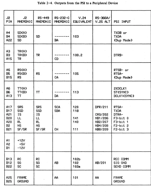
Pinouts for an RS-449 cable are shown in table 2-6. For high data rates and long cable lengths, 1 DO-ohm termination resistors (stored on the PSI card near socket U 1 06) should be inserted in sockets R27 and R28. See figure 2-1 for socket locations. Inserting these resistors causes the following signals to be terminated: RD, RT, CS, ST, DM, and RR. In some configurations, it may be desirable to connect signals R T and ST in parallel. This causes the terminating resistors to be paralleled also, resulting in 50-ohm termination. To avoid this and keep the termination impedance at 100 ohms, a 6 -pin termination resistor can be used in socket R 2 7. This leaves pins 1 and 2 of the socket uncon-nected so that only one termination resistor is used.
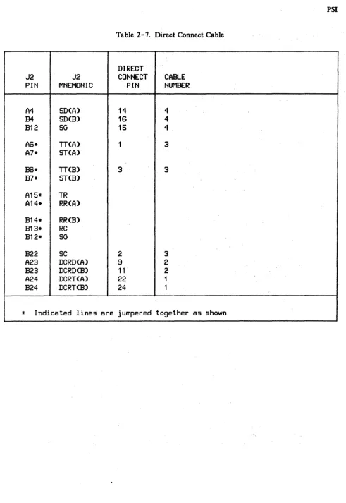
Direct Connect Cable
Optically isolated receivers are provided on the PSI for read data and receive timing. By using a direct connect cable, computer-to-computer communication can be accomplished up to a distance of 1000 meters. For short cable lengths, or when connected to HP 1000 Series Computers, jumpers W5 and W6 should be removed from the PSI card (socket U8I, see figure 2-1). This places a current-limiting resistor in the input circuit to prevent over driving the receivers.
See table 2-7 for the direct connect cable.
NOTE
PSI
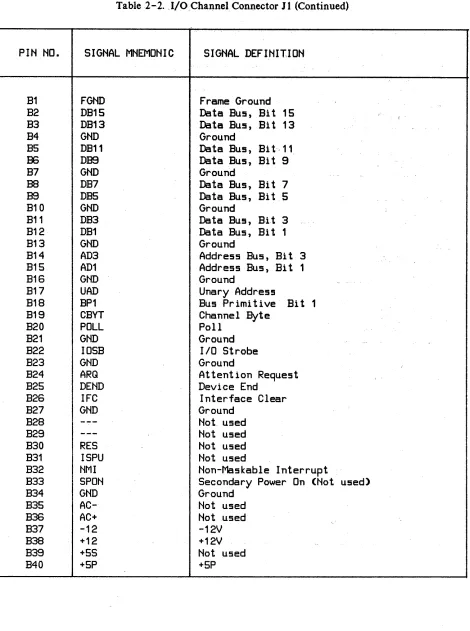
Table 2- 2. I/O Channel Connector J 1
PIN NO. SIGNAL MNEMONIC SIGNAL DEFINITION
A1 FGND Frame Ground
A2 DB14 Data Bus, Bit 14
A3 DB12 Data Bus, Bit 12
A4 GND Ground
AS DB10 Data Bus, Bi t 10
A6 DBS Data Bus, Bi t 8
A7 GND Ground
A8 DES Data Bus, Bi t 6
A9 DB4 Data Bus, Bi t 4
A10 GND Ground
A11 DB2 Data Bus, Bi t 2
A12 DBO Data Bus, Bi t 0
A13 GND Ground
A14 AD2 Address Bus, Bi t 2
A15 ADO Address Bus, Bi t 0
A16 GND Ground
A17 DOUT Data Out
A18 BPO Bus Primitive Bit 0
A19 CEND Channel End
A20 SYNC Synchronize
A21 GND Ground
A22 CCLK Conmon Clock
A23 GND Ground
A24 BR Burst Request
A25 DBYT Device Byte
A26 MYAD My Address
A27 GND Ground
A28
---
Not usedA29
---
Not usedA30
---
Not usedA31 RES Not used
A32 PFW Power-Fail Warning (Not used)
A33 PPON Primary Power On
A34 GND Ground
A35 AC- Not used
A36 AC+ Not used
A37 -12 -12V
A38 +12 +12V
A39 +5S Not used
Table 2 -2.· J/OChannel. Connector J 1 (Continued)
PIN NO.
SIGNAL MNEMONIC
SIGNAL DEFINIT.ION
B1
FGND
Frame Ground
B2
DB1S
Data Bus, Bi t 15
B3
DB13
Data Bus, Bit 13
B4
GND
Ground
B5
DB11
Data Bus, Bi
t,11
J36
DBS
Data Bus, Bit 9
B7
GND
Ground
B8
DB7
Data Bus, Bi t
7BS
DBS
Data Bus, Bi t 5
B10
GND
Ground
B11
DB3
Data Bus,
Bit 3B12
DB1
Data Bus, Bi t 1
B13
GND
Ground
B14
AD3
Address Bus, Bit
3B15
AD1
Address Bus, Bit 1
B16
GND
Ground
B17
UAD
Unary Address
B18
BP1
Bus Primitive Bi
t1
B19
CBYT
Channel Byte
B20
POLL
Poll
B21
GND
Ground
B22
IOSB
liD Strobe
B23
GND
Ground
B24
ARQ
Attention Request
B25
DEND
Device End
B26
IFC
Interface Clear
B27
GND
Ground
B28
---
Not used
B29
---
Not used
B30
RES
Not used
B31
ISPU
Not used
B32
NMI
Non-Maskable Interrupt
B33
SPON
Secondary Power On (Not used)
B34
GND
Ground
B35
AC-
Not used
B36
AC+
Not used
B37
-12
-12V
B38
+12
+12V
B39
+5S
Not used
PSI
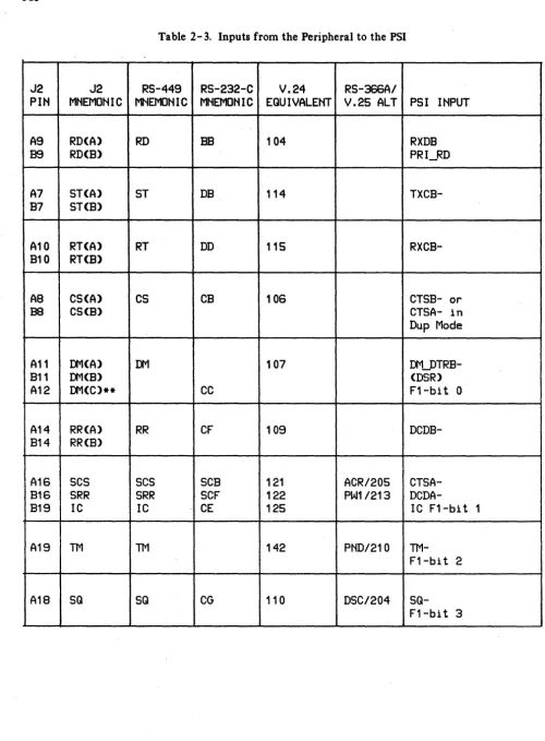
Table 2- 3. Inputs from the Peripheral to the PSI
J2
J2
RS-449
RS-232-C
V.24
RS-366AI
PHi
MHEMONIC MNEMONIC MNEMOHIC EQUIVALENT V.25 ALT PSI INPUT
A9
RD(A)
RD
BE104
RXDB
B9
RD(B)
PRI~DA7
ST(A)
ST
DB
114
TXCB-B7
ST(B)
A10
RT(A)
RT
DD
115
RXCB-B10
RT(B)
AS
CS(A)
CS
CB
106
CTSB- or
B8
CS(B)
CTSA- in
Dup Mode
A11
DM(A)
DM107
DM_DTRB-B11
DM(B)
(DSR)
A12
DM(C)**
CC
F1-bit 0
A14
RR(A)
RR
CF
109
DCDB-B14
RR(B)
A16
SCS
SCS
SCB
121
ACR/205
CTSA-B16
SRR
SRR
SCF
122
PW1/213
DCDA-B19
IC
IC
CE
125
IC F1-bit 1
A19
TMTM
142
PHD/210
TM-F1-bit 2
A1S
SQ
SQ
CG
110
DSC/204 [image:19.618.58.558.56.735.2]Table 2-3. Inputs from the Peripheral to the PSI (Continued)
J2
J2
RS-449
RS-232-G
V.24
RS-366AI
PIN
MNEMONIC MNEMONIC MNEMONIC EQUIVALENT V.25 ALT PSI INPUT
RXDA
B18
SRD
SRD
SEE
119
DLO/203
SEC_RD
F1-bit 4
A23
DCRD(A)
B23
DCRD(B)
RD
BE104
RXDB
A24
DCRT(A)
B24
DCRT(B)
RT
DD
115
[image:20.617.68.553.98.746.2]PSI
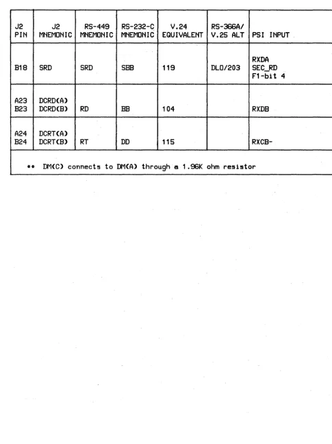
Table 2-4. Outputs from the PSI to a Peripheral Device
J2
J2
RS-449
RS-232-C
V.24
RS-366AI
PIN
MNEMONIC MNEMONIC MNEMONIC EQUIVALENT V.25 ALT PSI INPUT
A4
SD(A)
TXDB or
B4
SD(B)
SD
---
103
TXDA
A22
SD
BA
(Dup Mode)
A3
TR(A)
B3
TR(B)
TR
---
108.2
DTRB-A15
TR
CD
AS
RS(A)
RTSB- or
B5
RS(B)
RS
---
105
RTSA-B15
RS
CA
(Dup Mode)
AS
n(A)
2XDCLK1
B6
n(B)
IT ---113
ST(SYNC)
A13
n
DA
DCLK1(SYNC)
A17
SRS
SRS
SCA
120
DPR/211
RTSA-B17
SSD
SSD
SBA
118
TXDA
A21
IS
IS
CRQ/202
DTRA-B20
LL
LL
141
NB1/20S
F3-bit 0
A20
RL
RL
140
NB2/207F3-bit 1
B2
NS
NS
NB4/208F2-bit 2
B21
SF/SR
SF/SR
CH
111
NBS/209
F2-bit 3
A1
+12V
A2
+5V
B1
-12V
B13
RC
RC
102b
REC COMM
B12
SG
SG
AB
102
AB/201
SIG GND
B22
SC
SC
102a
SEND COI"1'1
A25
FRAME
AA
101
AA
FRAME
[image:21.617.66.554.80.700.2]Table 2-5. RS-232-C Cable Connections
J2
J2
RS-232-C
RS-232-C
PIti
MNEMONIC
PIN
MNEMONIC
*
---
1AA
A22
SD
2
BA
A9
RD(A)
3
BEB15
RS
4
CA
A8
CS(A)
5
CB
A12
O'-1(C)
6
CC
812**
SG
7
AB
87**
ST(8)
7
AB
88**
CS(B)
7
AB
89**
RD(B)
7
AB
810**
RT(B)
7
AB
811**
0'-1(B)
7
AB
813**
RC
7
AB
814**
RR(8)
7
AB
A14
RR(A)
8
CF
816
SRR(A)
12
SCF
A16
SCS(A)
13
SCB
817
SSD
14
SBA
A7
ST(A)
15
DB
B18
SRD(A)
16
SBB
A10
RT(A)
17
DD
A17
SRS
19
SCA
A15
TR
20
CD
A18
SQ(A)
21
CG
B19
IC(A)
22
CE
B21
SF/SR
23
CH
A13
IT24
DA
* The shield is connected to chassis ground through a
decoupling capacitor in the connector hood.
· PSI
Table 2-6. RS-449 Cable
J2
J2
DB-37
RS-449
PIN
MNEMONIC
PIN
MHEMOHIC
PAIR NUMBER
B12
SG
19
SG10
B13
RC
20
RC
16
A3
TR(A)
12
TR(A)
1
B3
TR(B)
30
TR(B)
1
A11
DM(A)
11
IJw1(A)
9
B11
DM(B)
29
IJw1(B)
9
A4
SD(A)
4
SD(A)
2
B4
SD(B)
22
SD(B)
2
A9
RD(A)
6
RD(A)
7
B9
RD(B)
24
RD(B)
7
A6
TT(A)
17
neAl
4
B6
TT(B)
35
nCB)
4
A7
ST(A)
5
ST(A)
5
B7
ST(B)
23
ST(B)
5
A10
RT(A)
8RT(A)
8B10
RT(B)·
26
RT(B)
8
AS
RS(A)
7
RS(A)
3
B5
RS(B)
25
RS(B)
3
AS
eS(A)
9
eS(A)
6B8
eS(B)
27
eS(B)
6
A14
RR(A)
13
RR(A)
11
B14
RR(B)
31
RR(Bl
11
B19
Ie
15
IC
13
B20
LL
10
LL
14
A20
RL
14
RL
14
A18
SQ
33
SQ
12
A19
TM
18
TM13
B22
SC
37
SC
16
A21
IS
28
IS
15
B21
SF/SR
16
SF/SR
15
[image:23.620.71.556.56.763.2]Table 2-7. Direct Connect Cable
DIRECT
J2
J2
CONNECT
CABLE
PIN
MNEMONIC
PIN
NUMBER
A4
SD(A)
14
4B4
SD(B)
16
4B12
SG
15
4A6*
n(A)
1
3
A7*
ST(A)
B6*
n(B)
3
3
B7*
ST(B)
A15*
TR
A14*
RR(A)
B14*
RR(B)
B13*
RC
B12*
SG
B22
SC
2
3A23
DCRD(A)
92
B23
DCRD(B)
11
2
A24
DCRT(A)
22
1
B24
DCRT(B)
24
1 [image:24.615.75.567.37.751.2]PSI
INST ALL A TION
I
CAUTIONI
ALWAYS ENSURE THAT THE POWER TO THE
COMPUTER IS OFF BEFORE INSERTING OR
REMOVING THE PSI CIRCUIT CARD AND CABLE. FAILURE TO DO SO MAY RESULT IN DAMAGE TO THE PSI.
I
CAUTIONI
SOME OF THE COMPONENTS USED ON THE PRINTED CIRCUIT CARD ARE SUSCEPTIBLE TO DAMAGE BY STATIC DISCHARGE. REFER TO THE
SAFETY CONSIDERATIONS INFORMATION AT
THE FRONT OF THIS MANUAL BEFORE
HANDLING THE CARD.
Install the PSI as follows:
1. Determine if your computer system can supply the power needed for the PSI card. Refer
to table 1-1 in Section I for power requirements.
2. Verify that the memory configuration jumpers are configured correctly for the EPROMs/RAMs installed on the card.
3. Install the card in the appropriate slot in the computer. Refer to the computer system in-stallation manual to determine the correct slot. When installing the card, use care not to damage components or traces on the card or on adjacent cards. Press the PSI card firmly into place.
I
CAUTIONI
BE SURE TO INSTALL THE DIAGNOSTIC TEST HOOD SO THAT ITS COMPONENT SIDE (THE SIDE WITH THE LED) HAS THE SAME ORIENTATION AS THE COMPONENT SIDE OF THE PSI RJE CARD. DAMAGE TO THE PSI RJE CARD CAN RESULT IF THE TEST HOOD IS INSTALLED INCORRECTLY.
START-UP
To start up and verify correct operation of the PSI, perform the following:
1. Turn on computer system power.
2. A self-test is contained on the card. The host computer system determines if the self-test is run automatically at power-on or must be invoked by the user. Refer to the appropriate manual for your system for a description of self -test initiation.
a. If the diagnostic test hood is not installed when the self -test executes, the LED located on the card should light briefly and go out. This indicates that the card passed self -test. If the LED does not light at all, the card is defective. If the LED stays on, the card did not pass self-test. For either of these latter two cases, it is recommended that you return the card to Hewlett-Packard; refer to the next paragraph for reshipment information. If you wish to perform maintenance on the card, however, refer to Sections 5, 6, and 7 for maintenance in-formation, replaceable parts lists, and schematic logic diagrams, respectively.
b. If the diagnostic test hood is installed when the self -test executes, the conditions in step 2.a. should occur, plus the LED located on the diagnostic test hood should light briefly and go out
simultaneously with the card's LED. If either LED (the one mounted on the card and the one
mounted on the diagnostic test hood) does not light at all, or lights and stays on, the causes are the same as in step 2.a.
3. Refer to your system documentation for information on using the PSI in your system.
RESHIPMENT
If the PSI is to be shipped to Hewlett-Packard for any reason, attach a tag identifying the owner and indicating the reason for shipment. Include the part number of the PSI.
PRINCIPLES OF OPERA TION
1-~---~~
FUNCTIONAL DESCRIPTION
A functional block diagram of the PSI is shown in figure 3-1. Reference will also be made to the schematic logic diagram contained in Section VI, figure 6-1. Note that figure 7 -1 consists of four sheets. References to this figure will be as follows: All, 6-1; C23, 6-1; D37, 6-1, etc., where the first digit (1, 2, 3, or 4) refers to the sheet number; the combination of letters A through E and numbers 11 through 48 (A 11, D 3 7, etc.) refer to the quadrants on the indi vid ual sheets; and 6 - 1 refers to the figure number. For example,
JqUadrant
All
L
sheet 1Jquadrant
D37
L
sheet3
Circuitry on the PSI card consists of a Backplane Interface Circuit (BIC) gate array and its sup-port circuits, a Z-80B microprocessor (CPU), up to 16K bytes of EPROM in two sockets, a Z-80 Counter Timer Circuit (CTC), a Memory Interface Circuit (MIC) gate array, 48K bytes of dynamic RAM, and a Z-80 Serial I/O circuit with associated multiplexer, modem control, and receiver and transmitter circuits.
The heart of the PSI card is the Z-80B CPU (U64, see A22, 6-1), which through a program stored in EPROM controls the functions of the card.
The Backplane Interface Circuit (BIC) (U41, see A14, 6-1) is a custom gate array integrated cir-cuit which controls the communication and handshaking within the I/O channel (backplane). The BIC is accessed by the Z-80B CPU as an I/O device for control information, and through Direct Memory Access (DMA) for data transfer to memory.
t:
m
I
40
...
(II
i
(II
~
a::
Q
~
6
elc
Z-80A CPU ue4
EPROM US1
8K
EPROM/RAM
8K U71
eTC U4-3
.... IC
ues
(DNA)
48K fWt4 UDO-U07
SlO U74
RECEIVERS/DRIVERS
U115,U116,U126 U111-U11 .... U121-U12J
Figure 3-1. PSI Functional Block Diagram
t:
m
I
GO
U1
::I
m
~
PSI'
The Serial I/O Circuit (SIO, U74, see A26, 6-1) and its associated multiplexers, modem control, and receivers and drivers, provides serial data communications and control lines to the frontplane connector J2.
System Clocks
Three synchronized system clocks (1.8432 MHz, 3.6864 MHz, and 7.3728 MHz), all derived from the 14.7456 MHz clock signal CCLK+ (see E21, 6-1), perform the following functions:
1.8432 MHz: Provides input to the CLK/TRG pins on the CTC to generate baud rates and system timing intervals.
3.6864 MHz: Used to provide a system clock to the Z-80B CPU, the SIO, MIC)cand CTC.
7.3728 MHz: Drives the MIC.
Memory Address Space
The Z-80B CPU address space of 64K bytes is divided into several sections as shown in figure 3-2.
The first 8K bytes of address space is reserved for ROM-based memory. See Section II for details on EPROMs that can be used. The second 8K bytes of address space can also use the same types of ROMs or, alternatively, can use static RAMs.
Eight positions (UDO through UD7) are provided on the PSI card for 64K by 1 dynamic RAMs. Because the Z-80B can only address 64K bytes of memory, only 48K bytes of dynamic RAM (memory locations 3FFFH through FFFFH) can be accessed by the Z-80 due to overlapping of ROM and dynamic RAM address space. The remaining 16K bytes of dynamic RAM can be accessed by the MIC under DMA control only.
The type of EPROM or static RAM which is used in each of the EPROM sockets on the PSI card must be configured by the 8-position Memory Configuration jumper (U81, see B33, 6-0. See Section II for details.
1/0
Address Space
64K
FFFFH
-
-
DFFFH
48K
-
64K
-
BFFFH
DYNAMIC
RAM
-
-
9FFFH
(48K USED)
32K
--
-
7FFFH
-
-
5FFFH
16K
3FFFH
8K EPROM
or
8K
.STATIC RAM
1 FFFH
8K EPROM
OOOOH
. MEMORY MAP
PSI
Table 3-1. I/O Address 'Space
I/O ADDRESS LINES
I/O PORT
I/O PORT FUNCTION
7 6 5
43 2
10
ADDRESS
READ/WRITE
POWER UP SWITCH
1 1 1 1
X X0 0
FO H
RO
MODEM STATUS INPUT
1 1 1
1 X X0 1
F1 H
RO
CONTROL LATCH
1 1 1
1 X X 10
F2 H
WO
MODEM LATCH
1 1 1
1 X X1
1F3 H
WO
MIC REG 0 CONFIG
1 1 1 0 0 0 0 0
EOH
RW
MIC REG 1 B HI ADDR
1 11 0 0 0
01
E1 H
WO,
MIC REG 2 B LO ADDR
1 11 0 0 0 1 0
E2 H
WO
MIC REG 3 B CONFIG
1
11 0 0 0 1 1
E3 H
RW
MIC REG 4 B LENGTH
1 1
10 0
10 0
E4 H
RW
MIC REG 5 B PORT ADDR
11
10 0
1 01
E5 H
RW
MIC REG 6 A HI ADDR
1 1
10 0
1 10
E6 H
WO
MIC REG 7 A LO ADDR
11 1
0 01 1 1
E7 H
WO
MIC REG 8 A CONFIG
11
10 1 0 0 0
E8 H
' RW
MIC REG 9 A LENGTH
1 1 1
01 0 0
1E9 H
RW
MIC REG 10 A PORT ADDR
11
10 1 0 1 0
EA
R
RW
MIC REG 11 INT VECTOR
1
1 10 1 0 1
1EB H
RW
CTC CH 0 IRQF
1 1 0
1 X X0 0
DO H
RW
CTC CH 1 2XDCLK1
1
10 1
XX 0
1D1 H
RW
CTC CH 2 DCLK2
1 1 0 1
XX 1 0
D2 H
RW
CTC CH 3 GEN PURPOSE
1 1 0 1 X X 1 1
D3 H
RWI
BIC REG 0 DATA
BIC REG 1 COMMAND
1 0 1 1
1 0 1 1 X 0
X0 0 0
01
BO H
B1 H
RW
RO
BIC REG 1 SUBCH ADDR
1 0 1 1
X0
01
B1 H
WO
BIC REG 2 ORDER
1 0 1 1 X 0 1 0
B2 H
RO
BIC REG 2 STATUS
1 0 1 1 X 0 1 0
B2 H
WO
BIC REG 3 BIC STATUS
1 0 1 1
X0 1 1
B3 H
RO
BIC REG 3 BIC CONTROL
1
01 1
X0 1 1
B3 H
WO
BIC REG 4 CONFIG
1 0 1 1 X
10 0
B4 H
RW
BIC REG 5 INTR LATCH
10 1 1 X
1 01
B5 H
RW
BIC REG 6 INTR'MASK
1 0 1 1
X1 1 0
B6H
RW
SID SEC CH A DATA
01 1 1 X
X0 0
70 H
RW
SID SEC CH A CONTROL
01 1 1
X X 01
71 H
RW
SID PRI CH B DATA
0
11 1
XX 1 0
72 H
RW
Serial
1/0
Controller
(510/2)
The Z-80 S10/2 (U74, A26, 6-1) is a programmable serial I/O controller with two independent full-duplex channels. Each channel has separate control and status lines for modems, and each channel can be independently programmed for synchronous or asynchronous operation. On the PSI card, channel B is the primary channel and can be operated synchronously or asynchronously, while channel A is the secondary channel and can be operated only in asynchronous mode.
SIO REGISTERS. Each SIO channel has an I/O addressable port for data transfer and for control in-formation. For control information there are three read registers and eight write registers available. The functions performed by the registers are shown in table 3-2.
SIO MODEM CONTROL AND STATUS BITS. The modem control and status bits of the SIO are used as defined in table 3-3. In addition, the WAIT/READY lines (W/RDYA- and W/RDYB-) lines should be set to READY for use with the DMA channels of the MIC.
The way that the SIO channels are configured is dependent on the modem control latch U 1 05 (see D27, 6-1), bits 0 through 4. Details are provided in the following paragraphs.
PSI CARD MODES OF OPERATION
The PSI card is capable of ten operational modes of operation and twelve self -test modes. The modes are listed later in tables 3-4 through 3-7.
The following paragraphs describe the signals and conventions used in those tables.
The modes of operation are numbered by using the binary value that is written to the Modem Control register (U8S, E27, 6-1) by data bits DO through D3 (DIR_CON, DUPLEX, SYNC, and INT_TIME). Bit D4 (SELFTEST) is set to 1 (false) for operational modes and 0 (true) for testing modes.
CONTROL LINES. The control lines are defined for use as follows;
INT _TIME: 1
=
use internal clocking source (DCLK 1) for channel B transmit data.0= use external clocking source (ST) for channel B transmit data.
or 0
=
use external clocking source (RT or DCRT) for channel B receive data, or internalclocking (DCLK 1) when in SELFTEST mode.
This control line has affect only when SYNC is true.
PSI
,Table 3- 2., SIO Register 'Functions
... , .. ,
WRITE REGISTERS FUNCTION
WRO Contains register pOinters, CRC initialization
information, initialization conmandsfor operating modes
WR1 Transmit/receive interrupt and data transfer
mode definition
WR2 Interrupt vector (channel B only)
WR3 Receive parameters and controls
WR4 Transmit/receive miscellaneous parameters and
modes
WRS Transmi t parameters and control!!
WR6 Synchronization character or SDLC address
field
WR7 Synchronization character or SDLC flag
READ REGISTERS FUNCTION
RRO Transmit/receive buffer status, interrupt
status, and external status
RR1 Special receive condition status
Table 3-3. SIO Modem Control and Status Bits
--OUTPUTS
CONNECTOR
REGISTER
SIO
J2NAME
AND BIT NO.
I/O ADDR
C
0
N RTSA-
SRS
SECONDARY REQUEST TO SEND WR REG 5 BIT 1
71H
T DTRA-
IS
IN SERVICE
WR REG 5 BIT 7
71 H
R RTSB-
RS
REQUEST TO SEND
WR REG 5 BIT 1
73 H
o
DTRB-
TR
TERMINAL READY
WR REG 5 BIT 7
73 H
L
INPUTS
S
T CTSA-
SCS
SECONDARY CLEAR TO SEND
RD REG 0 BIT 5
71 H
A DCDA-
SRR
SECONDARY RECEIVER-READY
RD REG 0 BIT 3
71
H
T CTSB-
CS
CLEAR TO SEND
RD REG 0 BIT 5
73 H
U DCDB-
RR
RECEIVER READY
RD REG BIT 3
73 H
S
2XDCU<1 IT
ASYNC
SIO TXCB RXCB
2)(ocu(1
-1
DlV BY 2SYNC EXT CLOCK
ST _ _ .... SIO
~---~~CB
RT _ _ _ _ _ _ -I
. > - - - t RXCa
Figure 3-4. SYNC EXT CLOCK Configuration
2XDCLK1 DIV BY 2
SYNC
INT CLOCK
SIO ""---f TXCB
RT _ _ _ -I
~---f RXCB IT
Figure 3-5. SYNC INT CLOCK Configuration
[image:35.615.66.600.53.758.2]DUPLEX:
o -
normal 510 operationTXCB TXCB- TXDB SDATA RXCB
RXCB-RXDB RXDB
CTSB CTSB- RTSB- RS
CHANNEL B CHANNEL A
DCLK2 TXCB- TxDA SSD
TXC8-SRD RXDA
SCS CTSA- RTSA- SRS
- FAST DUPLEX operation
TXCB TXC8- TXDB SOATA RXCB TXCB- RECEIVE
RXDB RXOB ONLY
CTSB CTS8- RTSB- RS
CHANNEL B CHANNEL A
TXCA- SEND TXDA SSO RXCA- ONLY
SRD RXDA RTSA- SRS
[image:36.613.79.554.38.747.2]
PSI
The following discussion applies to figure 3-6.
DUPLEX: 0 • normal SIO operation 1 = FAST DUPLEX mode
In normal operation, channel B is the Primary send and receive channel, while channel a is the Secondary send and receive channel. In FAST DUPLEX mode, channel B becomes the Primary receive channel, and channel A becomes the Primary transmit channel;
the secondary channel is not available. This mode allows both available DMA
chan-nels to be used for data transfer in both directions simultaneously in order to attain higher data transfer rates.
DIR_CON: 0 = MODEM operation. In this mode, the normal drivers and receivers are available
for use.
1 = Direct Connect operation. This mode is intended for use in direct computer-to-computer
connections where optical isolation is desired to prevent ground currents due to ground potential differences between the computers.
In direct connect mode, optically isolated receivers are used for both receive data (DeRD) and receive timing (DCRT). A special cable which only has Send Data (SO), Terminal Timing (TT), Receive Data (DCRD), and Receive Timing (DCR T), is used for this mode. This cable also loops back TT to ST, and TR to RR. The Direct Connect multiplexer (U 104, A 44, 6 -1) loops back DTRB to DM and RS to CTS.. These connections allow the same firmware to operate in modem mode or direct connect mode.
SELFTEST: 1:1 Normal operation.
o
= Self-Test mode. In this configuration, channel A data is looped back to channel A, and channel B data is looped back to channel B. In addition, DCLK 1 is, sent to TT and toRXCLK. This allows internal loopback in all asynchronous modes with internal
timing. A diagnostic loop back hood allows testing in synchronous modes with external timing.
OPERATIONAL MODE DEFINITIONS. Definitions of the operational modes are as follows:
MODE 0,1:
MODE 2:
MODE 3:
MODE 4,5:
Modem Asynchronous. Channel B clocked by 2XDCLK 1 and Channel A clocked by DCLK2.
Modem Synchronous External Clock. Channel B clocked by ST and RT. Channel A clocked by DCLK2.
Modem Synchronous Internal Clock. Channel B clocked by DCLKI and RT. Channel A clocked by DCLK2.
MODE 7:
MODE 8,9:
MODE 10:
MODE 11:
MODE 12, 13:
MODE 14:
MODE 15:
Modem Fast Duplex Synchronous Internal Clock. Channel B
receive channel and Channel A transmit channel. Channel B
clocked by R T and Channel A clocked by DCLK 1.
Direct Connect Asynchronous. Channel B receives DCRD and
clocked by 2XDCLK 1. Channel A clocked ·by· DCLK 2.
Direct Connect Synchronous External Clock. Channel B receives
DCRD and clocked by ST and DCR T. ST has no source so this mode is not usable. Use Mode 11.
Direct Connect Synchronous Internal Clock. Channel B receives DCRD and clocked by DCLKI and DCRT. Channel A clocked by DCLK2.
Direct Connect Fast Duplex Asynchronous. Channel B receives
DCRD only and Channel A transmits only. Both clocked by 2XDCLKI.
Direct Connect Fast Duplex Synchronous External Timing.
Channel B recei ve channel and Channel A transmi t channel.
Channel B clocked by DCRT and Channel A clocked by ST. ST
has no source so this mode is not usable. Use mode 1 5.
Direct Connect Fast Duplex Synchronous Internal Timing.
Channel B receive channel (DCRD) and Channel A transmit
channel. Channel B clocked by DCR T and Channel A clocked by DCLKI.
SELF-TEST MODE DEFINITIONS. Definitions of self-test modes areas follows. In all cases, SDA T A is tied to a MARK condition.
MODE STO, 1:
MODEST2:
MODE ST3:
MODEST4, 5:
MODEST6:
Modem Asynchronous. Channel B clocked by 2XDCLK 1 and
Channel A clocked by DCLK 2.
Modem Synchronous External Clock. Channel B clocked by ST and R T. Channel A clocked by DCLK2. Must use loopback hood.
Modem Synchronou;s Internal Clock. Channel B clocked by
DCLK 1. Channel A clocked by DCLK 2.
Modem Fast Duplex Asynchronous. Channel B receive channel
and Channel a transmit channel. Both clocked by 2XDCLKl.
Modem Fast Duplex Synchronous External Clock. Channel B
MODEST8,9:
MODESTIO:
MODE STIl:
MODE STI2, 13:
MODESTI4:
MODEST1S:
PSI
Direct Connect Asynchronous. Channel B clocked by 2XDCLK 1. Channel A clocked by DCLK2.
Direct Connect Synchronous External Clock. Channel B clocked by ST and OCR T. ST has no source so loopback hood must be used.
Direct Connect Synchronous Internal Clock. Channel B clocked by DCLKI. Channel A clocked by DCLK2.
Direct Connect Fast Duplex Asynchronous. Channel Band Channel A clocked by 2XDCLK 1.
Direct Connect Fast Duplex Synchronous External· Timing.
Channel B receive channel and Channel A transmit ch~nnel.
Channel B and Channel A clocked by DCLKI when used with loopback hood.
Direct Connect Fast Duplex Synchronous Internal Timing. Channel B receive channel and Channel A transmit channel. Channel B clocked by DCLKI and Channel A clocked by DCLKI.
MODEM CONTROL. PSI card modes of operation (described in the preceding. paragraphs) are controlled by the modem control lines (see D and E28, 6-1). The possible modes and the states of the control lines are shown in tables 3-4 through 3-7.
Table 3-4. Modem Control Multiplexer ~- Modem Mode
MULTIPL-XER OUTPUTS
MODE
CNTRL SDATA TXCB- RXDB- RXCB- RS-
CTSB-
DM-
RXDA RXTXCA-
CTSA-MODEM
1000X TXDB 2X
RD
2X
RTSB-
CS-
DM-
SRD DCLK2
SCS-ASYNC
MODE
DCLK1
DCLK1
0, 1
MODEM
10010 TXDB ST .
RD
RT
RTSB-
CS-
DM-
SRD DCLK2
SCS-
M
SYNC
MODE
U
EXT
2
X
I
N
MODEM
10011 TXDB DCLK1 RD
RT
RTSB-
CS-
DM-
SRD DCLK2
SCS-
P
SYNC
MODE
U
INT
3T
S
MODEM
1010X TXDA 2X
RD
2X
RTSA-
CS-
DM-
SRD 2X
CS-DUPLEX MODE
DCLK1
DCLK1
DCLK1
ASYNC
4, 5MODEM
10110 TXDA ST
RD
RT
RTSA-
CS-
DM-
SRD ST
CS-DUPLEX MODE
SYNC
6EXT
MODEM
10111
TXDA DCLK1 RD
RT
RTSA-
CS-
DM-
SRD DCLK1
CS-DUPLEX MODE
SYNC
7INT
\
I /\ I
I
PRIMARY CHANNEL
SECONDARY CHANNEL
CONTROL LINES
=
(SELFTEST, DIR_CON, DUPLEX, SYNC, I NT_TIME>
[image:40.618.63.555.65.681.2]PSI
Table 3-5. -Modem Control Multiplexer -- Direct Connect Mode
MULTIPLEXER·OUTPUTS
MODE
CNTRL SDATA TXCB- RXDB RXCB- RS-
CTSB-
I:fw1-RXDA RXTXCA-
CTSA-DIRECT 1100X TXDB 2X
DCRD 2X
RTSB- RTSB- DTRB- SRD DCLK2
SCS-CONNECT MODE
DCLK1
DCLK1
ASYNC
8, 9DIRECT 11010 TXDB ST
DCRD DCRT RTSB- RTSB- DTRB- .SRD DCLK2
SCS-CONNECT MODE
SYNC
10
««(DO NOT USE THIS MODE»»>
M
EXT
U
X
DIRECT 11011 TXDB DCLK1 DCRD DCRT RTSB- RTSB- DTRB- SRD DCLK2
SCS-CONNECT MODE
N
SYNC
11
P
INT
U
T
S
DIRECT 1110X TXDA 2X
DCRD 2X
RTSA- RTSA- DTRB- SRD 2X
RTSA-CONNECT MODE
DCLK1
DCLK1
DCLK1
DUPLEX 12,13
ASYNC
DIRECT 11110 TXDA ST
DCRD DCRT RTSA- RTSA- DTRB- SRD ST
RTSA~CONNECT MODE
DUPLEX 14
SYNC
««<DO NOT USE THIS MODE»»>
EXT
DIRECT 11111 TXDA DCLK1 DCRD DCRT RTSA- RTSA- DTRB- SRD DCLK1
RTSA-DUPLEX MODE
SYNC
15
INT
\
I
"
II
PRIMARY CHANNEL
SECONDARY CHANNEL
[image:41.612.68.553.79.731.2]Table 3-6. Modem Control MUX: Modem Self-Test Mode
SELF-
MUX OUTPUTS
TEST
. MODE
CNTRL SDATA TXCB- RXDB RXCB- RS-
CTSB-
Il"1-RXDA RXTXCA-
CTSA-MODEM
OOOOX MARK 2X
TXDB 2X
RTSB- CS-
Il"1-TXDA DCLK2
SCS-ASYNC
MODE
DCLK1
DCLK1
STO,1
MODEM
00010 MARK ST
TXDB RT
RTSB- CS-
Il"1-TXDA DCLK2
SCS-SYNC
MODE
<DCLK1>
<DCLK1>
EXT
ST 2
«<USE ONLY WITH DIAGNOSTIC TEST HOOD»>
MODEM
00011
MARK DCLK1 TXDB DCLK1 RTSB- CS-
Il"1-TXDA DCLK2
SCS- M
SYNC
MODE
U
INT
ST 3
X
MODEM
0010X MARK 2X
TXDA 2X
RTSA- CS-
Il"1-TXDA 2X
CS-
I
DUPLEX MODE
DCLK1
DCLK1
DCLK1
N
ASYNC
ST4,S
P
U
T
S
MODEM
00110 MARK ST
TXDA RT
RTSA- CS-
Il"1-TXDA ST
CS-DUPLEX MODE
<DCLK1>
<DCLK1>
<DCLK1>
SYNC
ST 6
I·EXT
«<USE ONLY WITH DIAGNOSTIC TEST HOOD»>
MODEM
00111
MARK DCLK1 TXDA DCLK1 RTSA- CS-
Il"1-TXDA DCLK1
CS-DUPLEX MODE
SYNC
ST 7
INT
\
I /\
,
IPRIMARY CHANNEL
SECONDARY CHANNEL
[image:42.615.59.548.73.753.2]PSI
Table 3-7. Modem Control MUX: Direct Connect Self-Test Mode
SELF-
MUX OUTPUTS
TEST
MODE
CNTRL SDATA TXCB- RXDB RXCB- RS-
CTSB- DM-
RXDA RSTXCA- CTSA
DIRECT 0100X MARK 2X
TXDB 2X
RTSB- RTSB- DTRB- TXDA DCLK2
SCS-CONNECT MODE
DCLK1
DCLK1
ASYNC
ST8,9
DIRECT 01010 MARK ST
TXDB DCRT RTSB- RTSB- DTRB- TXDA DCLK2
CONNECT MODE
<DCLK1>
<DCLK1>
SYNC
ST 10
EXT
«<USE ONLY WITH DIAGNOSTIC TEST HOOD»>
DIRECT 01011 MARK DCLK1 TXDB DCLK1 RTSB- RTSB- DTRB- TXDA DCLK2
CONNECT MODE
SYNC
ST 11
INT
DIRECT 0110X MARK 2X
TXDA 2X
RTSA- RTSA- DTRB- TXDA 2X
CONNECT MODE
DCLK1
DCLK1
DCLK1
ASYNC
ST 12,
ST 13
SCS-SCS-
M
U X
RTSA- I
N
P U
T
~ ________ ~ ______ +-__ ~ ______ +-__ ~ ______ ~ __ ~ __ ~ ____ ~ __ ~ ____ ~ __ ~S
DIRECT 01110 MARK ST
TXDA DCRT RTSA- RTSA- DTRB- TXDA ST
CONNECT MODE
<DCLK1>
<DCLK1>
<DCLK1>
DUPLEX ST 14
SYNC
EXT
«<USE ONLY WITH DIAGNOSTIC TEST HOOD»>
I
DIRECT 01111 MARK DCLK1 TXDA DCLK1
CONNECT MODE
RTSA-IRTSA-,DTRB- TXDA DCLK1
DUPLEX ST 15
SYNC
INT
RTSA-\~
______________
~~____________ --JI\
_______
r -_ _ _ _ _ '- I I
[image:43.617.64.553.58.758.2]Table 3-8. Modem Status, Port FI (Input Only)
BIT MNEMONIC TRUE RS-449
RS-232-C
CCITI RS-366
0
Jlw1J)TRB
1DATA MODE
CC DATA SET READY (DSR) 107
*
1
TERMINAL RDY CD DATA TERMINAL RDY
108.2
**
1
IC
1INCOMING CALL CE RING INDICATOR
125
2
TM 1TEST MODE
CI SIGNAL RATE IND
1421PND
112
3
SQ
1SIG QUALITY
CG SIGNAL QUALITY
110
COS
4
SEC_RD
0
SEC REC DATA SEE SEC REC DATA
119
DLO(1)
5
RDY
1
READY LINE FROM BIC
6
PRI_RD
0
RD OR DCRD (USED FOR X.21>
7
NIC
NO CONNECTION
* --
Modem mode
[image:44.620.63.555.92.742.2]PSI
Table 3-9. Control Latch, Port F2 (Output Only)
BIT MNEMOtiIC TRUE
FUtiCTIOti
RS-366
0
H-IT_TIME
1USE ItiTERtiAL CLOCK Iti SytiC MODE/tiOT EXT CLOCK
---1
SytiC
1SytiCHROtiOUS MODE/tiOT ASytiCHRONOUS MODE
---2
DUPLEX
1FAST DUPLEX MODE/NOT NORMAL MODE
---3
DIR_CON
1DIRECT COtitiECT MODE (OPTO-ISOLATED
---RECEIVERS)/tiOT tiORMAL MODE
4
SELFTEST
0COtitiECTS TXDA TO RXDA AtiD TXDB TO RXDB
---5
LED
0"TURtiS Oti LED ItiDICATOR
,"---6
XMITEti
1ENABLE DIFFERENTIAL TRANSMITTERS (SD, TR,
---ST, TT)
7
N/C
tiD CONNECTION
[image:45.617.68.557.105.749.2]Table 3-10. Modem Latch"PortF3 (Output Only)
BIT MNEMONIC TRUE
FUNCTION
RS-366
0
LL
1LOCAL LOOP BACK-
NB1 .
1
RL
1
REMOTE LOOP BACK
NB2
.
3
SF/SR
0SELECT FREQUENCE/SELECT RATE
NBS
NOTE:
All of the above lines are set to 0 at power-upCounter Timer Circuit (CTC)
The eTC (U43, A24, 6-1) provides four independent counter/timer channels. In the PSI card, these channels provide the following functions:
Channel 0 - - RQHDF DMARQl (DMA ReQuest channell, which is RDY-)
hold-off time from ZC/TOO.
Channel 1 - - 2XDCL Kl: SIO channel B (primary channel) baud rate generator.
Channel 2 -- DCLK2 SIO channel A (secondary channel) baud rate timer.
Channel 3: General purpose system timer.
NOTE
[image:46.618.44.563.88.398.2]PSI
The CTC has two modes of operation: Counter mode and Timing mode. In Timing mode, an external clock of 1.8432 MHz is used as a clock source. In Counter mode, the system clock of 3.6864 MHz is used with a prescale of either 16 or 256. A programmable divider is used to divide the input clock and is given as the value N.
Table 3-11. Synchronous Baud Rate Generation
TIMER SOURCE N 2XDCLK1 FREQ BAUD RATE
1.8432 MHz PHI CTC 2 921.6 KHz 460.8 KHz
Input to CTC 3 614.4 KHz 307.2 KHz
(Counter mode) 4 460.8 KHz 230.4 KHz
5 368.6 KHz 184.3 KHz
6 307.2 KHz 153.6 KHz
16 115.2 KHz 57.6 KHz
18 102.4 KHz 51.2 KHz
24 76.8 KHz 38.4 KHz
32 57.6 KHz 28.8 KHz
48 38.4 KHz 19.2 KHz
96 19.2 KHz 9.6 KHz
192 9.6 KHz 4.8 KHz
3.6864 MHz and 32 7200 Hz 3600 Hz
DIV 16 Prescale 36 6400 Hz 3200 Hz
(Timer mode) 48 4800 Hz 2400 Hz
64 ' 3600 Hz 1800 Hz
72 3200 Hz 1600 Hz
96 2400 Hz 1200 Hz
128 1800 Hz 900 Hz
3.6864 MHz and 12 1200 Hz 600 Hz
DIV 256 prescale 24 600 Hz 300 Hz
(Timer mode) 36 400 Hz 200 Hz
48 300 Hz 150 Hz
65 220 Hz 110 Hz
72 200 Hz 100 Hz
96 150 Hz 75 Hz
144 100 Hz 50 Hz
NOTE: In sync mode, ,2XDCLK1 is divided by 2 before going to
[image:47.618.69.557.100.736.2]Table 3-12. Asynchronous Baud R~te generation
.
TIMER SOURCE 1'1' 2XDCLK1 FREQ BAUD RATE
1.8432 MHz input 1 1843.2 KHz 115.2 KHz
to CTC (Counter 2 921.6 KHz 57.6 KHz
mode) 3 614.4 KHz 38.4 KHz
6 307.2'KHz 19.2 KHz
12 153.6 KHz 9.6 KHz
24 76.8 KHz 4.8 KHz
32 57.6 KHz 3.6 KHz
48 38.4 KHz 2.4 KHz
64 28.8 KHz 1.8 KHz
96 19.2 KHz 1 .2 KHz
128 14.4 KHz 900 Hz
192 9.6 KHz 600 Hz
3.6864 MHz System 3 76.8 KHz 4.8 KHz
clock divided by 4 57.6 KHz 3.6 KHz
16 prescale (Timer 6 38.4 KHz 2.4 KHz
mode) 8 28.8 KHz 1.8 KHz
12 19.2 KHz ·1.2,KHz
16 14.4 KHz 900 Hz
24 9.6 KHz 600 Hz
48 4.8 KHz 300 Hz
96 2.4 KHz 150 Hz
107 2153.3 Hz 134.5 Hz
(0.06% error)
131 1758.8 Hz 110 Hz
(0.07% error)
192 1 .2 KHz 75 Hz
3.6864 MHz System 1 14.4 KHz 900 Hz
clock divided by 3 4.8 KHz 300 Hz
256 prescale (Timer 5 2.88 KHz 180 Hz
mode) 6 2.4 KHz 150 Hz
9 1 .6 KHz 100 Hz
12 1 .2 KHz 75 Hz
18 800 Hz 50 Hz
[image:48.623.62.548.70.703.2]PSI
1/0
Channel (Backplane) Interface
The I/O channel, or backplane, interface consists of the Backplane Interface Circuit (BIC, U41, A14, 6-1) and buffers UII through Ul4 (A13 and C17, 6-0.
The BIC is an I/O addressable port to the Z-80B CPU and handles byte-to-word conversion and backplane handshaking. To the Z-80B CPU, the BIC appears as a set of ten registers which are read only, write only, and bi-directional. -To the I/O bus, theBIC appears as a set of six registers which also are read only, write only, and bi-directional.
The BIC registers available to the Z-80B are I/O mapped to hexadecimal addresses BO to B6 as shown in table 3-1, I/O address space.
The contents of the BIC registers are shown in figure 3-7.
Memory Interface Circuit (MIC)
The MIC (U65, A32, 6-1) is a custom CMOS gate array which provides the following functions:
Controls up to 64K by 8 of dynamic RAM
Controls up to 16K by 8 of EPROM and/or static RAM
Two programmable DMA channels
Vectors backplane interrupts for Z-80B CPU
, .. :. ' ':
ADDR READ -~: - ' 'WRITE
80
I :
':
:D~TA:
:
:
I
7 0
COMMAND SUBCHANNEL' ADDRESS
I
:OP~09E
1
:EXT:EN~
I
I
I
I
I'1'
S~8 :AD~R
17 0 7 0
81 OPCODES: 07 == PRESENT ADDRESS
o
== AST 1 == AEK 2=
esc
3
=
RES 4 == RSCORDER STATUS
I
?PC:OO~
l
:EXT:EN~
1I
?PC:OD~
l
:EXT~N~
,I7 0 7 0
82 OPCODES: OPCODES
o
== lOY 6 == RDo
== RFC5
==seR
1 == OLD 7 == WO 1 == AES 6 == DOD
2 == PAU 8 == RTS 2 == RES 7 == PER 3
=
DIS 9=
WTC 3 == ABO 8 == ERT4-
=
RS 10=
RES 4 -= DLF5 == WC 11 -= CtC
"
BIC STATUS BIC CONTROL
I
iF~~
1
:ST~TU~
I
I
ff
l I
~TR~BE~
I
7 0 7 0
83 07 -4 == IIF TYPE 03 == CDC
03 == DCL 02 == NMI
02 == CAR 01 == STP
01 == SSW DO == FCL
DO == DSW
[image:50.618.63.556.32.734.2]PSI
AD DR READ WRITE
CONFIGURAnON 07 : I END
S4
I
I
I
r1
~FO :CO~F
I
06 =
sn
05 - 510
7 0
07 - SRE INTERRUPT LATCH 03 - FFR
85 06 : I .Fe
I
I
I
r1
I
I
I
I
02 - RQA05 - NUK 01 - CUD
04 - END 7
a
DO - ORO07 - SRE INTERRUPT MASK 03 - F"FR
86 06
=
RESI
r
I
rl I
1 11
02=
RQA05 - NUK 01 - CMO
04 - END 7
a
DO = ORO [image:51.617.62.604.39.747.2]MIC REGISTER 0 - CONFIGURATION.
EO
MIC CONFIGURATION
1_
Ix~ I~D
I
1
I I
1 1
Bit 7
=
ll'12
Bit 6
=
XNT
Bit 5
=
DEND
Bits 4 - 0
7
DMA B request select (1
=
ll'1AR2, 0
=
DMAR1)
External Interrupt Enable (1
=
ENABLE)
Disable XEND .(1
=
DISABLE),
Not used
MIC REGISTER 1 - CHANNEL B HIGH MEMORY ADDRESS.
El CHANNEL 8 HIGH MEMORY ADDRESS
I I
:
HIGH :ORDE~ AD~RESS
:7
Write only register
o
I I
MIC REGISTER 2 - CHANNEL B LOW MEMORY ADDRESS.
E2 CHANNEL 8 LOW MEMORY ADDRESS
I I :
LOW:OROE~ ADO~ESS
:I I
7
o
Write only register
MIC REGISTER 3 (HIGH BYTE COUNT) - CHANNEL B CONFIGURATION.
E3 CHANNEL 8 CONFIGURATION
I
OMSI
INSI
SOMI
SNTI
HIO~OER ~NGT~
Bit 7
=
]]'1BBit 6
=
1MB7
DMA Channel B Enable (1
=
ENABLE) DMA Channel B Transfer Direction(1
=
liD
to Memory, 0=
Memory toliD)
o
PSI
Bi t
Bi t
Bi t
Bi t
Bi t
Bi t
5 = Br:t1
4
=
BMT
DMA B Address Count Direction (1
=
Decrement, 0=
Increment)DMA B Interrupt Enable (1
=
Enable)3 =
MIC REGISTER 4 - CHANNEL BLOW BYTE COUNT.
E4
CHANNEL B LOW BYTE COUNT
I
I :
LOW:ORO~R ~GTH
I I I
<