ISSN: 2319-8753
I
nternational
J
ournal of
I
nnovative
R
esearch in
S
cience,
E
ngineering and
T
echnology
(An ISO 3297: 2007 Certified Organization)
Vol. 3, Issue 1, January 2014
Sub-Threshold Logic and Standard Cell Library
Alok Sahu
1, Geoffrey Eappen
2P.G. Student, Department of Electronics Engineering, SGGSIE&T, Nanded, (M.S.) India1 P.G. Student, Department of Electrical Engineering, DTI SGSITS, Indore (M.P.) India2
Abstract: This paper presents the sub-threshold logic and standard cell library for it. Standard cell library consists of basic gates as well as universal gates (INVERTER, EX-OR, NAND, NOR gate) in sub-threshold logic. The components of this library can be used to design any complex combinational circuit utilizing less power as compared to super-threshold one. Impact of sizing of nmos and pmos is also given in this paper. There is also a comparison between sub-threshold and super-threshold logic.
Keywords: Sub-threshold logic, standard cell library, sizing of mos.
I. INTRODUCTION
The demand for low power electronics is rising day by day. In this era of hand held devices long battery life is a very important criterion for electronics industries. Everyone wants long battery life for their device. This all started from the Moore’s Law. In 1965, Gordon Moore observed that the number of transistors that can be placed on a single IC (Integrated Circuit) of the same area has been doubling every two years [1]. It affected the semiconductor industry positively. Transistors shipped per year have increased exponentially as the average price per transistor has dropped off exponentially with the minimum feature size. An additional benefit of this scaling is the increased performance of circuits. From there The Integrated Circuits (ICs) world is accustomed till this point to following Moore’s Law. But unexpectedly process scaling has a number of problems which blocks to move on exponentially. Some of them are
Increased power dissipation
Increased complexity etc.
Main concern which hampers the further scaling of transistors is the issue of power dissipation. A chip consist of many energy storage elements, mainly capacitors, some that are required for computation (MOSFET device capacitances) and some that are a hindrance to circuit operation (parasitic capacitances). These capacitors are continually charged and discharged through resistive elements during circuit operation, resulting in energy dissipation in the form of heat. The amount of heat dissipated puts a restriction on the computational performance of the circuit. While shrinking of devices has reduced the amount of parasitic capacitance and this alleviates power dissipation problems. But the number of devices (dissipating power somewhat less) accommodated has been increased due to process scaling which results in more power dissipation as compared to previous one. As the more number of transistors are placed on a single chip, the sub- threshold leakage current becomes dominant factor of total power dissipation. Sub-threshold leakage current occurs when transistor is off. So the leakage current dissipates power, even when it is not doing any useful computations, in the form of heat. The MOS-FET threshold voltage VT decreases with
increase in the device junction temperature caused by this heat dissipation. The sub-threshold leakage currents are exponentially dependent on VT, increasing with decrease in VT. Thus increased on-chip temperatures cause more power
dissipation due to increased leakage currents and increased dissipation of heat. Another problem with aggravated on-chip temperature is that they can result in reduced operating life spans for the on-chip [2].
II. SUB-THRESHOLD LOGIC
As seen above the sub threshold current is present in our circuit, but is of no use. So let us use these threshold current for operation of our circuit. The idea of using threshold current for circuit is known as sub-threshold logic. Here the VDD of the circuit is set at a value lower than or equal to the threshold voltage of that
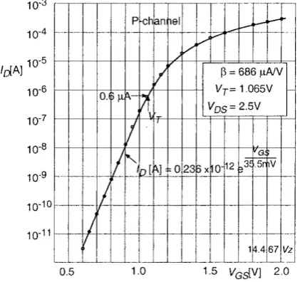
particular process technology, i.e. VDD≤ VT. Figure 2.1 shows the dependence of drain current (ID) on applied Gate to
Source voltage (VGS). This can be seen that below threshold voltage the current through the transistor is exponential in
ISSN: 2319-8753
I
nternational
J
ournal of
I
nnovative
R
esearch in
S
cience,
E
ngineering and
T
echnology
(An ISO 3297: 2007 Certified Organization)
Vol. 3, Issue 1, January 2014
never be in the linear or saturation region. This approach not only results in very low power consumption but it also utilizes leakage currents for computation.
Fig. 2.1: ID versus VGS plot, for 0.18µm process with VDD = 1.8V
The current through transistor in sub-threshold region for low VDS roll-off can be given as [3]:
0
exp
1 exp
GS T DS
D Sub threshold
th th
V
V
V
I
I
V
V
Where I0is the drain current, with VGS=VT , given as :
2
0 0 ox
1
thW
I
C
n
V
L
Making VDD lower reduces the current significantly. This reduced current is not sufficient to charge the load
capacitance fast enough. Due to this slow charging of load capacitance the circuit as a whole works becomes slow. To make the circuit fast we have to increase the current significantly upto a level enough to charge the load. For increasing the current, size of transistors are increased. Increasing the transistor size reduces the channel resistance upto certain extant but after this again the channel capacitance increases which becoming dominant factor for the fast operation of the circuit. This results in increased RC time constant of the circuit, Due to this increased RC time constant again circuit becomes slow. A proper sizing of transistor becomes very important because of the reasons given above.
III. STANDARD CELL LIBRARY
This section describes the design of various digital logic cells in sub-threshold. A methodology for designing a standard cell library in sub-threshold is discussed. All the logic cells are verified for their performance characteristics. One of the primary reasons to form a standard cell library is to use these cells as basic building blocks for larger circuits.
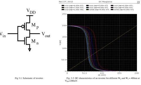
The standard cell library created consists of basic CMOS gates designed using 0.18µm technology. First, the basic CMOS inverter, shown in Figure 3.1, is analysed in detail and then, based on this analysis, the NAND and the NOR gates are designed.
ISSN: 2319-8753
I
nternational
J
ournal of
I
nnovative
R
esearch in
S
cience,
E
ngineering and
T
echnology
(An ISO 3297: 2007 Certified Organization)
Vol. 3, Issue 1, January 2014
inverters can be extended to explain the behaviour of more complex gates such as NAND, NOR, or XOR, which in turn form the building blocks for modules such as multipliers and processors.
Figure 3.1 and 3.2 show the schematic and dc characteristics of inverter respectively.
Fig 3.1: Schematic of inverter. Fig. 3.2: DC characteristics of an inverter for different Wp and Wn = 400nm at
VDD=200mV.
As seen from figure 3.2 the DC response is same as far as shape is concern. So now the question arises that what should be the width of PMOS and NMOS. We will see this now that how to decide the width.
B. Sizing of inverter
Traditionally, the PMOS is sized so that the drive strength is large enough to pull the output node up to a desired output high voltage level. Figure shows two cases where the decreased supply voltage, transistor sizing and process variations affect the inverter operation assuming an output swing of 10% to 90% of VDD [4].
Case 1: When 0 is applied to the input, then the PMOS is sized to pull-up the output node to 1. However, as the voltage supply of the inverter decreases, the idle current becomes significant. This results in a decreasing Ion/Ioff, and
causes the output node to drop. The Ion/Ioff ratio is used to indicate if a logic gate will function properly. Ion is defined to
be the drive current of the devices and decreases exponentially as supply voltage is lowered in sub-threshold operation. Ioff is defined as the idle current. The ratio is further reduced when considering process variations. The worst case
corner for the inverter is the fast NMOS/slow PMOS (FS) because the fast NMOS is leakier than the slow PMOS. Figure 3.3 shows at the FS corner, where is the minimum allowable PMOS width that still drives the output to 0.9 VDD
[4].
ISSN: 2319-8753
I
nternational
J
ournal of
I
nnovative
R
esearch in
S
cience,
E
ngineering and
T
echnology
(An ISO 3297: 2007 Certified Organization)
Vol. 3, Issue 1, January 2014
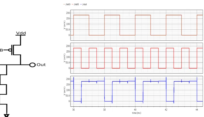
Fig 3.3: Determination of transistor width for minimum voltage operation. Fig 3.4: Transient response of inverter for VDD= 180mV.
C. NAND Gate
Figure 3.5 shows the schematic of NAND gate and figure 3.6 shows its transient response.
Fig 3.5: Schematic of NAND Gate. Fig 3.6: Transient response of inverter for VDD= 180mV.
ISSN: 2319-8753
I
nternational
J
ournal of
I
nnovative
R
esearch in
S
cience,
E
ngineering and
T
echnology
(An ISO 3297: 2007 Certified Organization)
Vol. 3, Issue 1, January 2014
Fig 3.7: Schematic of NOR Gate. Fig 3.8: Transient response of NOR Gate for VDD= 180mV.
E. X-OR Gate
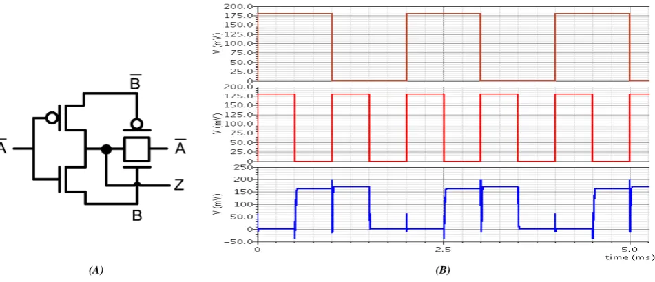
For designing a sub-threshold XOR logic cell, first we analyse traditional logic at low voltages. When the drives of this gate are lowered to the point that the on currents become comparable with the leakage currents then parallel leakage, stacked transistors, and sneak leakage effects affect functionality during low-voltage operation [4] [5]. Here we will see the methodology to minimize the implication of these effects.
(A) (B)
Fig 3.9: (A) Schematic of Tiny X-OR Gate and (B) Transient response of Tiny X-OR Gate for VDD= 180mV.
ISSN: 2319-8753
I
nternational
J
ournal of
I
nnovative
R
esearch in
S
cience,
E
ngineering and
T
echnology
(An ISO 3297: 2007 Certified Organization)
Vol. 3, Issue 1, January 2014
Fig 3.10: Tiny XOR Gate showing the parallel leakage with inputs A=0 and B=1.
Here since multiple devices are connected in parallel to a single circuit node, parallel leakage occurs in some cases. Parallel leakage occurs when the idle current of parallel devices reduces
I
on/I
off.
Specifically, several parallel offtransistors effectively increase the
I
off of the gate and degrade theI
on/I
off ratio. This degraded ratio can impact thefunctionality of the gate. Figure 3.10 show the case when A=0 and B=1. In this particular case there are 3 ‘off’ devices and only 1 ‘on’ device. This results in degradation of
I
on/I
off ratio [4][5]. That’s why for case (A=0, B=1) output Z =163mV and for (A=1, B=0) output Z= 170mV.
A transmission gate XOR (Figure 3.11) is a circuit where the number of parallel devices are minimized (or balanced) for minimum voltage operation. Because there are two devices pulling the output node high and two devices pulling low,
I
on/I
offratio is not degraded and the XOR is fully functional as shown in the simulation.
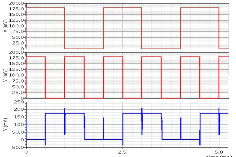
Fig 3.11: schematic of transmission XOR Gate. Figure 3.12: Transmission gate XOR Gate under the condition A=0, B=1.
ISSN: 2319-8753
I
nternational
J
ournal of
I
nnovative
R
esearch in
S
cience,
E
ngineering and
T
echnology
(An ISO 3297: 2007 Certified Organization)
Vol. 3, Issue 1, January 2014
IV. PERFORMANCE COMPARISON
A. POWER
The total power in a CMOS circuit is given by equation:
P
Total
P
Static
P
Dynamic2
1
2
C V
L DD
f
I V
SC DDI
Static DDV
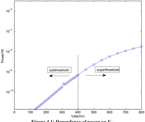
Where CL is the load capacitance, f is the frequency of operation, ISC is the direct path short circuit current arises when both NMOS and PMOS transistors are simultaneously active, conducting current directly from supply to ground [6]. α is the activity factor. As can be seen from Equation the total power consists of two major components: dynamic power and leakage power. Both these components reduce in magnitude as the supply voltage reduces.
Figure 4.1 shows the dependence of power dissipation upon supply voltage (VDD) for both sub-threshold as well as super-threshold region.
Figure 4.1: Dependence of power on VDD .
B. ENERGY
Energy is one of the important design metrics in digital circuits. The energy estimation in these circuits is given by Equation
Total Static Dynamic
E
E
E
2
1
2
C V
L DD
I
StaticV t
DD p
ISSN: 2319-8753
I
nternational
J
ournal of
I
nnovative
R
esearch in
S
cience,
E
ngineering and
T
echnology
(An ISO 3297: 2007 Certified Organization)
Vol. 3, Issue 1, January 2014
C. Frequency
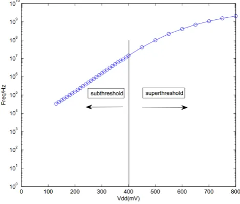
To understand the variation in frequency and power characteristics in super-threshold and sub-threshold regions, simulations of a seven-stage ring oscillator using an inverter chain were performed in IBM 65 nm technology node. Figure 4.2 shows the operating frequency dependence upon supply voltage (VDD) scaling.
Figure 4.2: Dependence of frequency on VDD
V. RESULT &CONCLUSION
As seen from the equation for the power and energy they are dependent on supply voltage (VDD) as a square function. So scaling the supply voltage will definitely reduce the power as well as energy. By observing the comparison we have seen that this reduction of supply strongly affects the speed of operation of the circuit.
REFERENCES
[1] Moore, Gordon E. "Cramming more components onto integrated circuits." (1965).
[2] Daasch, W. R., C. H. Lim, and G. Cai. "Design of VLSI CMOS circuits under thermal constraint." Circuits and Systems II: Analog and Digital Signal Processing, IEEE Transactions on 49.8 (2002): 589-593.
[3] Wang, Alice, Benton H. Calhoun, and Anantha P. Chandrakasan. Sub-threshold design for ultra low-power systems. Springer, 2006. [4] Wang, Alice, and Anantha Chandrakasan. "A 180-mV subthreshold FFT processor using a minimum energy design methodology."
Solid-State Circuits, IEEE Journal of 40.1 (2005): 310-319.
[5] A. Wang, B. H. Calhoun, and A. P. Chandrakasan, Sub-threshold design for ultralow-power systems. Springer Science+ Business Media, 2006.
[6] Veendrick, Harry JM. "Short-circuit dissipation of static CMOS circuitry and its impact on the design of buffer circuits." Solid-State Circuits, IEEE Journal of19.4 (1984): 468-473.