http://dx.doi.org/10.4236/am.2015.62037
Wave Iterative Method for Patch
Antenna Analysis
Pinit Nuangpirom, Surasak Inchan, Somsak Akatimagool
Department of Teacher Training in Electrical Engineering, King Mongkut’s University of Technology North Bangkok, Bangkok, Thailand
Email: [email protected], [email protected], [email protected]
Received 22 January 2015; accepted 10 February 2015; published 13 February 2015
Copyright © 2015 by authors and Scientific Research Publishing Inc.
This work is licensed under the Creative Commons Attribution International License (CC BY). http://creativecommons.org/licenses/by/4.0/
Abstract
Wave Iterative Method (WIM) is a numerical modeling for electromagnetic field analysis of mi-crowave circuits. Theories of transmission line, four terminal network and boundary condition are applied to developing WIM simulation that the physical electromagnetic wave is described to a mathematical model using GUI function of MATLAB. In applying, the microstrip patch antenna was analyzed and implemented. The research result shows that the WIM simulation can be used cor-rectly to analyze the electric field, magnetic field theory and return lose of sample patch antenna. The comparison of the WIM calculation agrees well with the measurement and the classical simu-lation.
Keywords
Wave Iterative Method, Electromagnetic Field Analysis, Patch Antenna
1. Introduction
Presently, numerical methods are important for scientists, engineers and researchers. The development and re-search are necessary for technical problem solving [1]-[4]. The basic Wave Iterative Method (WIM) is a full wave analysis that has been developed since 2001, and is suitable for microwave circuit analysis [5]-[9]. Evolu-tion of the WIM was developed to support microwave circuits such as waveguides [10] [11], filter circuits [7] and applied in telecommunication engineering education [8] [12]. The advantages of WIM algorithm are the in-tegration of theories of transmission line, two ports network and boundary conditions and iterative method that are weak definition to study.
2. Wave Iterative Method
wave and transmitted wave in the multi-layers planar structure. The electric field, magnetic field and network parameters of equivalent circuit are results that we want to solve and display.
2.1. Wave Equations
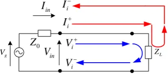
Transmission line is represented by equivalent circuit, as shown inFigure 1, where Vin and Iin are the voltage and current variables at the input ports, Vin
+
and Iin
+
are incident voltage and current wave, Vin
−
and Iin
−
are reflected voltage and current wave, respectively. The relationship between incident wave and reflected wave is defined as [13]
in in in
V =V++V−, (1) in in in
I =I+−I−. (2)
Considering the input port, as shown inFigure 1, normalized waves in Equations (1) and (2) are divided by 0
Z , thus we have
in in in
0 0 0
V V V
Z Z Z
+ −
= + , (3)
0 in 0 in 0 in
Z I = Z I+ − Z I−. (4)
The relation equation base on the incident wave (A) and reflected wave (B) is presented by
in
0 V
A B
Z = + , (5)
and
0 in
Z I = −A B (6)
where in
0 in 0
V
A Z I
Z
+
+
= = and in
0 in 0
V
B Z I
Z
−
−
= = .
Then, the input voltage and current equation can be written as
(
)
in 0
V = Z A+B , (7)
(
)
in 0 1
I A B
Z
= − . (8)
Rewrite the equations in the form of an electric field and current density that are as
(
)
0
E= Z A+B , (9)
(
)
0 1
J A B
Z
= − . (10)
[image:2.595.229.398.629.708.2]Equation (9) and (10) are the electric field and current density (or magnetic field) in following the wave equa-tion. The variable A (incident wave) and B (reflected wave) are the key parameters used in the WIM algorithm.
Figure 1. Transmission line circuit.
L
Z in
V
in
I
0
Z
g
V
i
I+
i
I−
i
V+
i
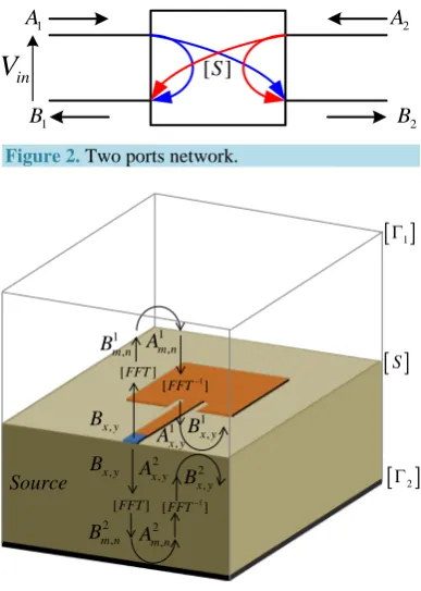
Considering, the scattering parameter (S) of a two ports network as shown inFigure 2, is defined in terms of wave variables as [14]
1 11 1 12 2
B =S A +S A , (11)
2 21 1 22 2
B =S A +S A . (12)
The S parameters defined by the incident and reflected wave are expressed as
1 1
11 2 12 1
1 2
2 2
21 2 22 1
1 2
when 0, when 0
when 0, when 0,
B B
S A S A
A A
B B
S A S A
A A
= = = =
= = = =
(13)
where An, Bn are the wave variables and An=0 that implies a perfect impedance match at port n. The wave definition is written as
1 11 12 1
2 21 22 2
B S S A
B S S A
=
. (14)
The parameters variable Sii is called the reflection coefficients at port i=1, 2, whereas Sij is the transmission coefficients of two ports network, where i≠ j and j=1, 2.
2.2. Wave Iterative Method (WIM)
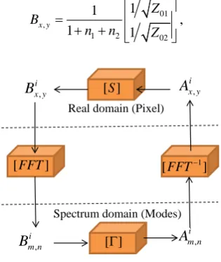
Wave propagation described by incident, reflected and transmitted waves is represented in the planar structure. We see that the waves will be reflected continuously, as shown inFigure 3.
In iterative procedure, the excited wave
( )
B( )x y, in the real domain (Pixel) of planar source is converted to the wave (i , )m n
B in the spectrum domain (Modes) by using the Fast Fourier Transform (FFT). Considering the upper and bottom side of metallic box, we obtain the wave (i , )
m n
A form reflection of the wave (i , ) m n
B by the reflection coefficient
( )
Γi . The wave ( , )i m n
A in the spectrum domain will be transformed to the wave ( )i, x y
A in the real domain by using the Invert Fast Fourier Transform (IFFT). At the planar structure situated between
in
V
1
A A2
1
B B2
[image:3.595.216.410.437.709.2][ ]S
Figure 2. Two ports network.
Figure 3. Wave propagation in planar circuit. ,
x y
B
[FFT] [FFT]
2 , m n B 2 , m n A , x y B 1 , m n B
[ ]
Γ2[ ]
Γ1[ ]
S1 , m n
A
1
[FFT−]
1
dielectric region (i) 1 and 2, the wave A( )ix y, will reflect to the wave B( )ix y, by the scattering parameter (S) of two ports equivalent network. Finally, the process of wave propagation will be repeated until the convergence of waves is solved.
The WIM procedure, as shown in Figure 4, is summarized by the following steps: 1) Define the excited wave B( )x y, of planar source.
2) Convert the waves in the real domain to the spectrum domain by the FFT: B(im n, )=
[
FFT]
( )
B( )ix y, .3) Apply the reflection coefficient
( )
Γn for reflected waves to obtain incident waves: ( )( )
[ ]
(( ) )
(
)
, ,
i i
i
m n m n
A = Γ B .
4) Transform the waves in the spectrum domain to the real domain by the IFFT: ( )( ), FFT 1
(
(( ), ))
i i
x y m n
A = − A . 5) Calculate the reflected waves using the scattering parameters of planar circuit: B( )( )x yi, =
[ ]
S( )
A( )( )ix y, . 6) Repeat step 2 to step 5 until the convergence of the network parameters are obtained.After testing the convergence at the k iterations, the tangential electric field and current density in the discon-tinuity using Equations (9) and (10), can be written as
( ), 0
(
)
k k k
i i i
x y
E = Z A +B , (15)
(, )
(
)
0k k k
i i i
x y
J = A +B Z . (16)
Thus, the admittance parameter of two ports network are obtained as
( ) ( )
,
, ,
x y
x y x y
J Y
E
=
∑
, (17)also, the impedance parameter can be written as
( ) ( )
,
, ,
x y
x y x y
E Z
J
=
∑
. (18)Finally, the scattering parameter of planar circuit is given by
[
][
]
10 0
S = Z −Z Z +Z − . (19)
The detail of mathematical operator in the WIM procedure, as shown inFigure 4 is represented as following.
2.2.1. Source Excitation Definition
The excited wave
( )
B( )x y, in the real domain of planar source can be written as01 ,
1 2 02
1 1
1 1
x y
Z B
n n Z
=
[image:4.595.236.394.522.709.2]+ + , (20)
Figure 4. Iterative procedure.
[FFT] [FFT−1]
[ ]Γ [ ]S
Real domain (Pixel)
Spectrum domain (Modes)
, i x y
B
, i m n
B ,
i m n
A
, i x y
where 0 1 01 Z n Z
= , 0
2 02 Z n
Z
= , 0
0 0
ri i
ri
Z µ µ
ε ε
= that is the characteristic impedance of dielectric layer i = 1, 2.
2.2.2. The Modal FFT and Modal IFFT Transform
For simplify the calculation of the generalized TEm,n, TMm,n mode wave description, the Modal FFT pair permits movement the transverse filed components from the real domain to the spectrum domain, the modal wave equa-tion in x direction can be defined as
( , ) ( ), 1 1 π π cos sin M N j
TE TM k
x j k x m n
j k
m x n y
B B a b = = =
∑∑
, (21)And also, the equation in y direction is defined as
( , ) ( ),
1 1
π π
sin cos
M N
TE TM k k
y j k y m n
j k
m x n y
B B a b = = =
∑∑
. (22)Thus, the modal transform matrix using WIM algorithm can be represented as
( ) ( ) , , , FFT TE
m n x
m n TM
y m n
B n b m a B
Q
B m a n b
B
−
=
. (23)
Similar, the Modal IFFT pair permits movement the modal filed components from the spectrum domain comeback to the real domain, the spatial wave equation in x direction can be defined as
( ,) 1 1 π π cos sin m n M N TE TM x x m n
m x n y
A A M N = = =
∑∑
, (24)And also, the wave equation in y direction is defined as
( ,)
1 1
π π
sin cos
y m n
M N TE TM y
m n
m x n y
A A M N = = =
∑∑
. (25)Thus, the spatial wave matrix using WIM algorithm can be represented as
( ) ( ) 1 , 1 , , 1 FFT TE m n x TM
y m n m n
A
A n b m a
A Q m a n b A
− − = −
, (26)
where
(
) ( )
, 2 2 , 1 2 m n m n ab Qm a n b
=
Φ + , ,
2, if , 0; 1, if , 0. m n
m n m n
≠
Φ = ≠
M, N refer the pixel or modes number, a, b
refer the metallic box dimension.
2.2.3. Reflection Coefficient (Γi) in the Spectrum Domain
The expression of reflection coefficient at the upper and bottom side of box in the spectrum domain is given by
0 ,
0 , 1
1
TE TM i m n TE TM
i TE TM
i m n Z Y
Z Y
−
Γ =
+ , (27)
where the TEm,n, TMm,n mode admittances in the metallic box are ,
0 TE m n r Y j γ ωµ µ
= , 0
,
TM r
m n
j Y ωε ε
γ
= respectively,
(
) (
2)
2 20
π π r
m a n b k
γ = + − ε , and k0=ω µ ε0 0.
2.2.4. Scattering Parameter (S) in the Real Domain
1
I I2
1
E E2
0 d=
1 2
E =E I1 I2
1
E E2
1 2
E =E
1 2 0
J +J =
1
r
ε εr2 1
I I2
1
E E2
0 d=
1 2
E =E
0
Z
0
E
1
Z Z2
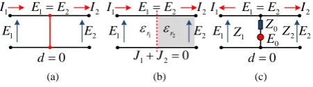
[image:6.595.201.427.87.150.2](a) (b) (c)
Figure 5.Equivalent circuit of discontinuity. (a) Metal region; (b) Dielectric region; (c) Source region.
Case 1, on the metal regions (M), we have the condition; E1=E2=0, thus the wave relation in the region 1 and 2 can be represented as
1 1 2 2 1 0 0 1 M M B A B A − = −
. (28)
Case 2, on the dielectric regions (D), we have the conditions; E1=E2 and 0J1+J2= , the wave relation can be represented as
2 2 2 1 1 2 2 2 2 2 1 2 1 1 2 1 1 1 D D n n
B n n A
B n n A
n n − = + + − + +
. (29)
Case 3, on the planar source regions (P), we have the condition; E1=E2=E0−Z0
(
J1+J2)
, the wave rela-tion can be represented as1 2 12
1 1 2 1 2 1
2
2 12 1 2
1 2 1 2
1 2 1 1 2 1 1 1 P P
n n n
B n n n n A
A
B n n n
n n n n
− + − + + + + = − − + + + + +
, (30)
where E0 refers the excited electric field and the Z0 refers the source internal impedance, and 01 02 Z n Z = , 0 1 01 z n Z
= , 0
2 02 z n
Z
= , and 12 0
01 02 z n
Z Z
= .
Finally, at the planar circuit in the real domain, the scattering parameters of wave equation are summarized on each printed surface region using Equations (23)-(25). The wave relation equation can be expressed as
1 1
2 2
B T U A
B V W A
=
. (31)
where
(
2)
(
)
1 2 2 1 2 1 1 1 1
n D n n P
T M n n n + − − + − = − + + + + ,
( )
(
12)
2 2 1 2 2 1 1
n D n P
U V M
n n n +
= = +
+ +
+ ,
(
2)
(
)
1 2 2 1 2 1 1 1 1
n D n n P
W M n n n + − − − + = − + + + + .
3. WIM Simulation Design
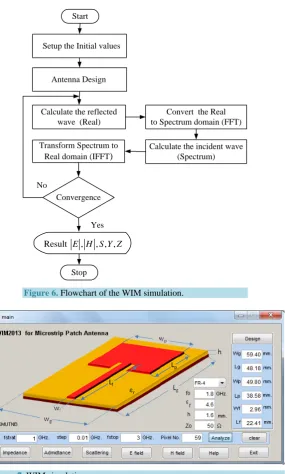
Computer aided design based on a graphical user interface (GUI) function of MATLAB® is developed using the Wave Iterative Method (WIM) algorithm. The WIM scheme consists of four parts as 1) setup the initial values, 2) design the patch antenna structures, 3) calculate the waves propagated in the spectrum (Modes) and real do-main (Pixel) using WIM algorithm, and 4) analysis the network parameters and electromagnetic distributions. The WIM simulation process can be presented inFigure 6.
The WIM simulation applied to simple patch antenna works in the following steps.
1) Start the WIM simulation program base on GUI function of the MATLAB, as shown inFigure 7.
2) Setup the usable values of calculation by using the “Setup” menu such as; operating frequency, desired printed circuit, dielectric constant value, characteristic impedance, etc.
3) Select the “Analysis” menu to design the microstrip patch antenna parameters using conventional antenna theories approach [14] [15].
Start
Calculate the reflected wave (Real)
Convergence
Stop
Calculate the incident wave (Spectrum) Transform Spectrum to
Real domain (IFFT)
No
Yes
Result ,E H S Y Z, , ,
Convert the Real to Spectrum domain (FFT) Antenna Design
[image:7.595.177.463.239.714.2]Setup the Initial values
Figure 6. Flowchart of the WIM simulation.
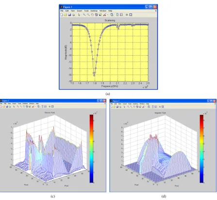
[image:7.595.198.428.246.518.2]4) Select the “Scattering” or “Impedance” or “Admittance” menu to calculate the scattering parameters of two ports network using the WIM algorithm for designed antenna analysis, an example is shown inFigure 8(a).
5) Select the “E- Field” menu to represent the electric field distributions using the WIM algorithm on the printed interface of planar circuit, as shown inFigure 8(b).
6) Select the “H- Field” menu to represent the magnetic field or current density distributions using the WIM algorithm on the printed interface of planar circuit, as illustrated inFigure 8(c).
7) Select the “Exit” menu to quit form the program.
4. Simulated and Experimented Results
An example of simple microstrip patch antenna is presented using the electromagnetic simulation base on the proposed Wave Iterative Method (WIM) algorithm. In this topic, we will introduce an antenna design tool, an efficiently WIM simulated results to compare to the IE3D software and measurement.
4.1. Microstrip Antenna Design
The optimal parameters of the simple microstrip patch antenna are designed at 1.8 GHz operating frequency. The FR4 printed board was implemented with the relative permittivity
( )
εr equal to 4.6, and the thickness of(a)
[image:8.595.90.538.295.708.2](c) (d)
dielectric layer is1.6 mm., The analyzed results using the WIM simulation program can be obtained correctly to compare the conventional antenna theories approaches [14] [15]. The printed circuit dimension of designed an-tenna is 49.8 × 38.58 mm2, as shown inFigure 9.
4.2. Electromagnetic Field Distributions
The simulation program has been developed using the WIM algorithm. Determination of the input E-filed of source excitation on the planar circuit, the computing electromagnetic field distribution will be propagated gradually on the planar structure. The evaluation of the electric and magnetic field distributions in term of itera-tion number at 1, 5, 10 and 200 rounds is appeared on the antenna structure, as shown inFigure 10. It was found that small iteration number, the electromagnetic field distributions on the planar structure are not completely and exactly. After testing the convergence with reasonable number of iterations, on the printed circuit, the norma-lized electric field peak is at the conductor edge, and minimum values are occurred in remote areas. On the other hand, the current density distributions on λ 2 long of conductor of each calculation have spread from source in to conductor area and will stabilize when the calculation is convergence (Approximately 200 rounds or more that depends on the designed circuit resolutions).
4.3. Return Loss Analysis of Patch Antenna
In the order to confirm the efficiency of the WIM simulation to compare the IE3D software and measurement, we will analyze and measure the return loss of the simple patch antenna using the N5230C network analyzer of
[image:9.595.162.461.335.439.2]
Figure 9. Microstrip patch antenna structure, where Wp = 49.8 mm; Lp = 38.58 mm; Wg = 59.40 mm; Lg = 48.18 mm; Wf = 2.96mm; Lf = 22.41 mm.
(a) (b) (c) (d)
[image:9.595.96.538.482.694.2]Figure 11. Experiment of the patch antenna.
Figure 12. Simulated and measured results of return loss.
Agilent Technologies, as shown inFigure 11.
The WIM simulated result of return loss of the designed patch antenna as shown inFigure 12, found that the center frequency is obtained at 1.8 GHz, and the −3 dB bandwidth is 180 MHz. Compared to the WIM simula-tion, theIE3D software and measurement of designed antenna are good agreement. Therefore, a little measure-ment errors were occurred, it may be the limitation of the experimeasure-ment set, the interface between coaxial probe and conductor strip, and also the planar structure different in the implemented process.
5. Conclusions
We have demonstrated the full wave analysis based on the developed Wave Iterative Method (WIM) algorithm to analyze the simple microstip patch antenna. The novel WIM algorithm can provide a reasonably good ap-proximation to the correct values of circuit parameters, and its accuracy is dependent on usable pixel size and mode number. Additionally, this algorithm has the advantage of representing the electromagnetic field on circuit structure. Finally, the contribution in this paper indicates the development of the novel WIM algorithm based on iterative method that can be used to analyze effectively in arbitrarily inhomogeneous region formations.
In the future, the proposed WIM algorithm will be also applied to MMICs, various planar circuit structures, passive circuit in the waveguide, and the electromagnetic solving for EMI/EMC problems.
References
[1] Carrasco, J.A. and Sune, V. (2011) A Numerical Method for the Evaluation of the Distribution of Cumulative Reward 38.5mm
49.8mm
48.2mm
59.4mm 22.4mm
till Exit of a Subset of Transient States of a Markov Reward Model. IEEE Transactions on Dependable and Secure Computing, 8, 798-809. http://dx.doi.org/10.1109/TDSC.2010.49
[2] Lezar, E. and Davidson, D.B. (2011) GPU-Accelerated Method of Moments by Example: Monostatic Scattering. IEEE Antennas and Propagation Magazine, 52, 120-135.
[3] Li, H., et al. (2010) Multi-Target Scattering Analysis Based on Generalized Higher-Order Finite-Difference Time- Domain Method. International Conference on Microwave and Millimeter Wave Technology (ICMMT), Chengdu, 8-11 May 2010, 88-90.
[4] Gao, X.-K., Chua, E.-K. and Li, E.-P. (2011) Application of Integrated Transmission Line Modeling and Behavioral Modeling on Electromagnetic Immunity Synthesis. IEEE International Symposium on Electromagnetic Compatibility (EMC), Long Beach, 14-19 August 2011, 910-915. http://dx.doi.org/10.1109/ISEMC.2011.6038438
[5] Akatimagool, S., Bajon, D. and Baudrand, H. (2001) Analysis of Multi-Layer Integrated Inductors with Wave Concept Iterative Procedure (WCIP). IEEE MTT-S International in Microwave Symposium Digest, 3, 1941-1944.
[6] Tellache, M. and Baudrand, H. (2011) Efficient Iterative Method for Characterization of Microwave Planar Circuits. 11th Mediterranean Microwave Symposium (MMS), Phoenix, 20-24 May 2001, 265-272.
[7] Hajlaoui, E.A., Glaoui, M. and Trabelsi, H. (2006) Analysis of Multilayer Microstrip Filter by Wave Concept Iterative Process. International Conference on Design and Test of Integrated Systems in Nanoscale Technology, Tunis, 5-7 September 2006, 150-153.
[8] Raveu, N., Prigent, G., Pigaglio, O. and Baudrand, H. (2010) Different Spectral Scale Level in the Wave Concept Iter-ative Procedure to Solve Multi-Scale Problems. IET Microwaves, Antennas & Propagation, 4, 1247-1255.
http://dx.doi.org/10.1049/iet-map.2008.0416
[9] Ji, W.-S., Luo, Q.-Z. and Yang F. (2010) Analysis of H-shaped Patch Antenna by Wave Concept Iterative Procedure (WCIP). International Conference on Microwave and Millimeter Wave Technology (ICMMT), Chengdu, 8-11 May 2010, 797-800.
[10] Akatimagool, S. and Choocadee, S. (2013) Wave Iterative Method for Electromagnetic Simulation. In: Zheng, Y., Ed., Wave Propagation Theories and Applications, InTech, Charpter14, 331-352.
[11] Tao, Q., Nie, Z.P. and Zong, X.Z. (2012) Numerical Solution of the Horn Antenna with Complex Structure. Interna-tional Symposium on Antennas, Propagation & EM Theory (ISAPE), Xi’an, 22-26 October 2012, 562-565.
[12] Husoy, J.H. (2003) Making a Case for Iterative Linear Equation Solvers in DSP Education. IEEE International Confe-rence on Acoustics, Speech, and Signal Processing (ICASSP’03), 6-10 April 2003, Vol. 3, 765-768.
[13] Liao, S.Y. (1988) Microwave Circuit Analysis and Amplifier Design. Prentice-Hall International Inc., Upper Saddle River.