NANORODS ARRAY FOR ULTRAVIOLET SENSOR
APPLICATION
SALINA BINTI MOHAMMAD MOKHTAR
FABRICATION OF TITANIUM DIOXIDE NANORODS ARRAYS FOR ULTRAVIOLET SENSOR APPLICATION
SALINA BINTI MOHAMMAD MOKHTAR
A thesis submitted in
fulfillment of the requirement for the award of the Degree of Master in Electrical Engineering
Faculty of Electrical and Electronic Engineering Universiti Tun Hussein Onn Malaysia
This thesis was dedicated to my parents; Mohammad Mokhtar bin Mohammad, Rabiah binti Ibrahim,
ACKNOWLEDGEMENT
First and foremost, I would like to thank my research supervisor, Assoc. Prof. Dr. Mohd Khairul bin Ahmad for his guidance and encouragement throughout the research. My thesis would not have been possible without his excellent supervision. I would like to express my sincere appreciation to my co-supervisor, Dr. Mohamad Hafiz bin Mamat for his advice and support for this research.
Many thanks to my colleagues in Microelectronic and Nanotechnology Shamsudin Research Centre (MiNT-SRC), particularly Noor Kamalia Abd Hamed, Fatin Izyani Mohd Fazli, Muhammad Luqman Mohd Napi, Asyikin Sasha Mohd Hanif, Nurliyana Mohamad Arifin, Ng Kim Seng, Nur Fakhriah, Sakinah Mohd Khalid, and others, for their help, motivation, kindness, and support during my studies. I also would like to thank Universiti Tun Hussein Onn Malaysia amd Ministry of Higher Education for the scholarship and financial support.
My special thanks to Prof. Masaru Shimomura and Prof. Kenji Murakami from Shizuoka University for their support of this research, including advice and research facilities. I gratefully acknowledge MiNT-SRC staffs, Ms. Isrihetty ans Mrs. Faezahana for their assistance in the lab.
LIST OF PUBLICATIONS
1. S. M. Mokhtar, M. K. Ahmad, N. M. A. N. Ismail, M. S. Mamat, F. I. M. Fazli, N. K. A. Hamed, M. L. M. Napi, N. S. Khalid, N. K. Seng. N. Zainal, S. C. Fhong, N. Nayan, & A. B. Suriani, “Fabrication Of Co/SnO2 On Glass
Substrate Using Spray Pyrolysis Deposition Technique With Variation Of Annealing Temperature”, ARPN Journal of Engineering and Applied Sciences (JEAS), vol. 11, no. 14, pp. 8873-8877 (2016).
2. S. M. Mokhtar, M. K. Ahmad, N. M. A. N. Ismail, A. B. Suriani, “Fabrication of Titanium Dioxide (TiO2) Nanorods Array with Various Reaction Times
Using One Step Hydrothermal Method”, ARPN Journal of Engineering and Applied Sciences (JEAS), (2017), (Submitted)
3. M. K. Ahmad, S. M. Mokhtar, C. F. Soon, N. Nafarizal, A. B. Suriani, A. Mohamed, M. H. Mamat, M. F. Malek, M. Shimomura, and K. Murakami, “Raman investigation of rutile-phased TiO2 nanorods/nanoflowers with various reaction times using one step hydrothermal method,” J. Mater. Sci. Mater. Electron. (2016).
4. M. L. M. Napi, M. F. Maarof, C. F. Soon, N. Nayan, F. I. M. Fazli, N. K. A.Hamed, S. M. Mokhtar, N, K, Seng, M. K. Ahmad, A. B. Suriani, & A. Mohamed, “Fabrication of Fluorine Doped Tin Oxide (FTO) Thin Films Using Spray Pyrolysis Deposition Method For Transparent Conducting Oxide”, ARPN Journal of Engineering and Applied Sciences (JEAS), Vol. 11, no. 14, pp. 8800-8804 (2016).
5. F. I. M. Fazli, A. N. Suhaimi, N. S. Khalid, N. K. A. Hamed, M. L. M.
Luqman, S. M. Mokhtar, N. K. Seng, N. Zainal, N. Nayan, S. C. Fhong, A. B. Suriani & M. K. Ahamd, “The Effects Of Annealing Temperature On
Properties Of Aluminium-Doped Tin Oxide (Al/SnO2) Thin Films Deposited
6. N. K. A. Hamed, R. Mahat, N. S. Khalid, F. I. M. Fazli, M. L. M. Napi, S. M. Mokhtar, N. K. Seng, S. C. Fhong, N. Nayan, A. B. Suriani, M. K. Ahmad, “Fabrication Of Co/SnO2 Thin Film for DSSC Using Spray Pyrolysis
ABSTRACT
Pure rutile titanium dioxide nanorods thin film for ultraviolet sensor application was fabricated on top of bare FTO substrates using hydrothermal method. TiO2 thin film
was developed by optimizing amount of titanium butoxide (TBOT) as a precursor, amount of hydrochloric acid, and hydrothermal reaction time. Basically, there were four properties studied; surface morphology, structural, electrical, and optical properties. Surface morphology of the sample was analyzed by using FESEM. XRD and Raman spectroscopy were used to analyze the structural properties of the thin film. Electrical and optical properties were studied using 2-point probe and UV-vis-NIR spectrophotometer. The first optimization step was to vary the amount of precursor used. Surface morphology of the sample shows that the nanorods growth starts at 3.5 mL of TBOT, and as the precursors increased, diameter and the thickness of the nanorods also increased. Both XRD and Raman show the peaks of FTO and rutile TiO2. Next, the hydrothermal reaction time was varied. Nanorods diameter and
thickness increase with increasing reaction time. XRD and Raman depict FTO and rutile TiO2 peaks produced. Lastly, the effect of using different amount of
hydrochloric acid used was studied. The diameter and thickness of the nanorods decrease as the HCl used increased. Thin film produced was rutile TiO2 confirmed
by both XRD and Raman spectra. The optimized amount of precursor, reaction time, and amount of HCl were obtained at 4.0 mL of TBOT, 16 hour, and 130 mL of HCl, respectively. Study on the optical properties of the TiO2 thin film shows absorption
on ultraviolet wavelength and not on visible wavelength. Electrical analysis shows that the electron flows through TiO2/FTO interface with conductivity of 0.167 S/m.
ABSTRAK
Filem nipis titanium dioksida (TiO2) nanorod bagi applikasi pengesan ultraungu telah
difabrikasi di atas tin oksida terdop fluorine (FTO) dengan menggunakan kaedah hidroterma. Filem nipis TiO2 telah dihasilkan dengan menggunakan titanium
butoksida (TBOT) sebagai pemangkin, asid hidroklorik, dan air ternyahion. Pada dasarnya, terdapat empat sifat yang dipelajari iaitu permukaan morfologi, struktur, elektrikal, dan optikal. Permukaan morfologi sampel telah dikaji dengan menggunakan FESEM. XRD dan Raman spektroskopi digunakan bagi mengkaji ciri struktur filem nipis. Ciri optikal dan elektrikal dikaji dengan menggunakan 2-point probe dan UV-vis-NIR. Kajian ini telah dijalankan dengan mengoptimumkan masa reaksi, jumlah pemangkin yang digunakan, dan jumlah asid hidroklorik yang digunakan. Proses optimasi yang pertama adalah dengan mempelbagai jumlah pemangkin yang digunakan. Permukaan morfologi menunjukkan bahawa penumbuhan nanorod bermula pada jumlah 3.5 mL TBOT, dan apabila jumlah pemangkin naik, garisan pusat dan ketebalah nanorod turut menaik. Kemudian, masa reaksi hidroterma telah dipelbagaikan. Garisan pusat dan ketebalan nanorod menaik apabila masa hidroterma dinaikkan. Yang terakhir, kesan menggunakan jumlah asid hidroklorik yang berlainan telah dipelajari. Garisan pusat dan ketebalah menurun apabila jumlah asid yang digunakan menaik. Nanorod TiO2 menunjukkan ciri
serapan yang bagus pada gelombang ultraungu. Analsis elektrikal menunjukkan bahawa elektron mengalir diantara permukaan TiO2/FTO dengan nilai konduksi
CONTENT
TITLE i
DECLARATION ii
DEDICATION iii
ACKNOWLEDGEMENT iv
LIST OF PUBLICATIONS v
ABSTRACT vii
ABSTRAK viii
TABLE OF CONTENTS ix
LIST OF FIGURES xiii
LIST OF TABLES xvii
LIST OF SYMBOL AND ABBREVIATIONS
xix
LIST OF APPENDICES xx
CHAPTER 1 INTRODUCTION 1
1.1 Research background 1
1.2 The properties of titanium dioxide 3
1.3 Problem statement 5
1.4 Research objective 5
1.5 Scope of the study 6
CHAPTER 2 LITERATURE REVIEW 7
2.1 Introduction 7
2.2 Titanium dioxide 7
2.2.1 Titanium dioxide nanorods array
2.3 Hydothermal 10
2.3.1 History of hydothermal 11
2.3.2 Fabrication of TiO2 nanorods
array using hydrothermal method
13
2.4 Ultraviolet sensor 16
2.4.1 Ultraviolet sensor using titanium dioxide nanomaterials
17
2.4.2 Ultraviolet sensor mechanism 18
CHAPTER 3 METHODOLOGY 22
3.1 Introduction 22
3.2 Substrate cleaning by sonicating method
23
3.3 Preparation of titanium dioxide solution for hydrothermal reaction
23
3.4 Fabrication of the titanium dioxide nanorods array via hydrothermal method
26
3.4.1 Fabrication of TiO2 nanorods
array using different amount of precursor
26
3.4.2 Fabrication of TiO2 nanorods
array using various reaction times
27
3.4.3 Fabrication of TiO2 nanorods
array using various amount of hydrochloric acid
27
3.4.4 Preparation of fabricated titanium dioxide
nanorods array for two-point probe current-voltage (I-V) measurement
28
3.5 Nanostructured TiO2 thin film
characterization method
29
3.5.1 Field-emission scanning electron microscopy
3.5.2 X-Ray diffraction 32
3.5.3 Micro-Raman spectroscopy 34
3.5.4 Ultraviolet-Visible-Near- Infrared (UV-vis-NIR) spectrophotometry
35
3.5.5 Two - point probe I-V measurement
37
3.5.6 Ultraviolet photocurrent measurement system
39
CHAPTER 4 RESULTS AND DISCUSSION 41
4.1 Introduction 41
4.2 Study on the effect of using different amount of precursor solution on titanium dioxide nanorods array
42
4.3 Study on the effect of using different hydrothermal reaction time on titanium dioxide nanorods array
49
4.4 Study the effect of using different amount of hydrochloric acid on titanium dioxide nanorods array
56
4.5 Titanium dioxide nanorods ultraviolet sensor
63
4.5.1 Electrical properties of the optimized sample
63
4.5.2 Optical properties of the optimized sample
65
4.5.1 Photocurrent properties of the optimized sample
66
CHAPTER 5 CONCLUSION 72
5.1 Introduction 72
5.2 Conclusion 73
REFERENCES 75
APPENDICES 84
LIST OF FIGURES
Figure 1.1: Electromagnetic spectrum showing the wavelength of three types of ultraviolet that is UVA, UVB, and UVC
2
Figure 1.2: The primitive cell unit for rutile TiO2 3
Figure 1.3: Schematic illustration of the formation mechanisms of the anatase and rutile crystal phase
4
Figure 2.1: TiO2 nanorods fabricated by (a) sol electrophoretic and
(b) sol-gel electrospinning methods
10
Figure 2.2: The mechanism of photoconduction in the TiO2-based
UV photoconductive sensor under both dark and UV illumination
22
Figure 3.1: Summarized of nanostructured TiO2 thin film preparation
and characterization
24
Figure 3.2: Summarized of cleaning substrate procedure 24
Figure 3.3: Autoclave used for hydrothermal process 26
Figure 3.4: FTO substrate before and after hydothermal reaction 26
Figure 3.5: Summarized of preparation of TiO2 solutions 27
Figure 3.6: The mask used for sputter-coater gold deposition 30
Figure 3.7: The auto-fine coater used to deposit gold on the sample 30
Figure 3.8: The FESEM equipment (JEOL-JSM 7600F) used to analyse the morphological and the cross-sectional images of the sample
32
Figure 3.9: Illustration of FESEM sample stage 33
Figure 3.10: FESEM’s (a) specimen stage control panel and (b) operation panel used to controlling screen sample images
Figure 3.11: XRD instrument (PANanalytical X-Pert3 Powder) used to
characterise the crystallinity of the samples
35
Figure 3.12: The Micro-Raman spectroscopy used to characterise the structural properties of the TiO2 nanorods array
36
Figure 3.13: Illustration of typical Raman spectra system 37
Figure 3.14: The vis-NIR spectrophotometers (Shimadzu UV-1800 240V) used to study the optical properties of the prepared nanorods arrays
38
Figure 3.15: Illustration of UV-Vis-NIR system 39
Figure 3.16: Two-point probe connected to the source meter used to identify the I-V characteristics of the sample
40
Figure 3.17: Close-up of the sample connected to the two-point probe 41
Figure 3.18: Electrochemical measuring unit used as a source of bias voltage
42
Figure 3.19: Photo-electrochemical instrument setup for measuring photocurrent
42
Figure 4.1: FESEM image of the commercial FTO as a reference 43
Figure 4.2: Surface morphology images of TiO2nanorods array
fabricated using different amounts of precursor from (a) 0.5, (b) 2.0, (c) 3.5 (d) 4.0, and (e) 5.0 mL of TBOT
45
Figure 4.3: Cross-sectional images of TiO2nanorods array fabricated
using different amounts of precursor from (a) 0.5, (b) 2.0, (c) 3.5 (d) 4.0, and (e) 5.0 mL of TBOT
45
Figure 4.4: Schematic diagram of TiO2 nanorods in different amounts
of precursor TBOT
46
Figure 4.5: XRD patterns of TiO2nanorods array fabricated using
different amounts of precursor from (a) 0.5, (b) 2.0, (c) 3.5 (d) 4.0, and (e) 5.0 mL of TBOT
47
Figure 4.6: Raman spectra of TiO2nanorods array fabricated using
different amounts of precursor from (a) 0.5, (b) 2.0, (c) 3.5 (d) 4.0, and (e) 5.0 mL of TBOT
48
Figure 4.7: Zoomed Raman spectra for TiO2 nanorods array
fabricated using (a) 0.5 and (b) 2.0 mL of TBOT
Figure 4.8: Surface morphology of TiO2nanorods array fabricated
with different hydrothermal reaction times from (a) 4, (b) 7, (c) 16, and (d) 24 hours, cross-sectional images of (e) 4, (f) 7, (g) 16 and (h) 24 hours hydrothermal reaction time
51
Figure 4.9: Growth mechanism of TiO2 nanorods fabricated using
different reaction time
52
Figure 4.10: XRD patterns of TiO2nanorods array fabricated with
different hydrothermal reaction time from (a) 4, (b) 7, (c) 16, and (d) 24 hour
53
Figure 4.11: Raman spectra of TiO2nanorods array fabricated with
different hydrothermal reaction times from (a) 4, (b) 7, (c) 16, and (d) 24 hour
55
Figure 4.12: Zoomed Raman spectra for TiO2 nanorods array
fabricated with 4 hours reaction times
55
Figure 4.13: Surface morphology of TiO2 nanorods array fabricated
with (a) 100, (b) 110, (c) 120, (d) 130, and (e) 140 mL of HCl
58
Figure 4.14: Cross-sectional area of TiO2 nanorods array fabricated
with (a) 100, (b) 110, (c) 120, (d) 130, and (e) 140 mL of HCl
59
Figure 4.15: Sketch diagram of TiO2 nanorods in different amounts of
hydrochloric acid
60
Figure 4.16: XRD patterns of TiO2nanorods array fabricated with (a)
100, (b) 110, (c) 120, (d) 130, and (e) 140 mL of HCl
61
Figure 4.17: Raman spectroscopy of TiO2 nanorods array fabricated
using (a) 100, (b) 110, (c) 120, (d) 130, (e) 140, and (f) 150 mL of HCl
63
Figure 4.18: Current-Voltage (I-V) plots on TiO2 surface and
TiO2/FTO interface of the optimized sample
64
Figure 4.19: The (a) transmittance and (b) absorbance spectra of the optimized sample
66
Figure 4.20: Indirect bandgap energy from Tauc’s plot 66
Figure 4.21: Photocurrent of the optimized sample with different bias voltage
67-69
Figure 4.22: Enlarged (a) rising and (b) decaying edges of the photocurrent
Figure 4.23: Schematic energy band diagram and working principle of the UV photosensor
LIST OF TABLES
Table 2.1: Comparison of the method used to grow TiO2 nanorods
10
Table 2.2: Evolution of hydrothermal technology with time
12
Table 2.3: Comparison of hydrothermal technique used to fabricate TiO2 nanorods array
16
Table 3.1: Preparation of TiO2 solution for
hydrothermal reaction
24
Table 3.2: Preparation of TiO2 solution for
hydrothermal reactionwith different amount of TBOT precursor
27
Table 3.3: Preparation of TiO2 solution for
hydrothermal reactionwith different reaction time
27
Table 3.4: Preparation of TiO2 solution for
hydrothermal reactionwith different amount of hydrochloric acid
28
Table 4.1: Summarised parameters used for optimization process
42
Table 4.2: Observed FESEM analysis with comparison to previous research
44
Table 4.3: Value of FWHM for TiO2 nanorods
array fabricated using different amounts of precursor
47
Table 4.4: Observed Raman shift with comparison to previous result
49
Table 4.5: Summarised parameters used for optimization process
50
Table 4.6: Observed FESEM with comparison to previous research
Table 4.7 Value of FWHM for TiO2 nanorods
array fabricated using different amounts of precursor
54
Table 4.8: Observed Raman shift with comparison to previous result
56
Table 4.9: Summarised parameters used for optimization process
57
Table 4.10: Observed FESEM with comparison to previous research
60
Table 4.11: Value of FWHM for TiO2 nanorods
array fabricated using different amounts of precursor
62
Table 4.12 Observed Raman shift with comparison to previous result
63
Table 4.13 The conductivity, resistivity, and sheet resistance value for different surfaces
64
Table 4.14 Photocurrent value, as well as the rise rime and decay time of the photocurrent
LIST OF SYMBOL AND ABBREVIATIONS
A - Cross sectional area
Au - Gold
CBD - Chemical bath deposition
cm - Centimeter
d - Diameter
DI - Deionized water
DSSC - Dye-sensitized solar cell
EMU - Electrochemical measuring unit
FE-SEM - Field-emission scanning electron microscope
FTO - Fluorine-doped tin oxide
GaN - Gallium nitiride
HCl - Hydrochloric acid
L - Length
O2 - Oxygen
R - Resistance
Rs - Sheet resistance
Si - Silicon
SiC - Silicon carbide
t - Thickness
TBOT - Titanium butoxide
TiO2 - Titanium dioxide
TTIP - Titanium isopropoxide
UV - Ultraviolet
V - Voltage
XRD - X-ray diffraction
ZnO - Zinc oxide
LIST OF APPENDICES
APPENDIX TITLE PAGE
A Gantt Chart 84
B UV Lamp
Datasheet
CHAPTER 1
INTRODUCTION
1.1 Research background
TiO2 has became known as a potential material to use in UV sensor applications. It
can strongly absorb UV light because it has an indirect [1] and wide band-gap energy. Conductivity of TiO2 rise when UV light is illuminated, making the electrons
from valence band excited to the conduction band. A signal produced, due to the excitation that given increase in conductivity, that is used for UV light detection. There are several TiO2 structures that can be produced such as microspheres,
nanoflowers, nanotrees, and nanobelts [2] depending on the technique used. Example of the techniques include chemical bath deposition (CBD), hydrothermal method, sol-gel method, and RF sputtering. However, solution-based techniques are favored in producing high-quality TiO2 as it is consuming low cost and therefore
allowing the fabrication of UV sensors at minimal price. Moreover, by the addition of a stabilizer or surfactant, the growth of TiO2 structure can be easily controlled. The
solution-based can also promotes the growth of TiO2 at low temperature with
large-scale, simple processing methods [3]. Highly crystalline rutile TiO2 has been
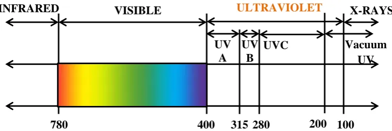
Photo-detection in the ultraviolet (UV) area has attracted attention due to its numerous applications in industry, instrument, and our daily life. Ultraviolet light is defined as a portion of the electromagnetic spectrum that includes visible light, radio waves, X-rays and microwave, with wavelength ranging from 100 to 400 nm that can be further subdivided to: Vacuum UV (100-200 nm), UVC (200-280 nm), UVB (280-315 nm), and UVA (316-400 nm) [9]. It has wavelength that is shorter than visible light, but longer than X-rays as shown in Figure 1.1. Ultraviolet light is used in various applications, including cancer therapy, chemical synthesis, jaundice treatment for new-born babies [10], and drug detection. However, overly exposed to overdose radiations can gives harm to human health. For example, overexposure to UV radiation can causes skin burning and possible skin cancer [11]. Nowadays, research on higher performance UV light sensor are continuously being developed as many situations requiring the monitoring of UV irradiation. Ultraviolet sensor is a device that measures UV light from the sun. it is used in wide range of applications including fire detection, industrial manufacturing, biochemical research, and environmental health monitoring. The traditional electrical UV sensor, which consist of a sensitive photodiode that generates a photocurrent when exposed to UV light, is well established. The current is then converted into a voltage signal and amplified for easier detection. The sensing element of the traditional UV sensor is the photodiode, which is commonly based on silicon.
Figure 1.1: Electromagnetic spectrum showing the wavelength of three types of ultraviolet that is UVA, UVB, and UVC
200
Vacuum UV
315 UV
A UV
B
UVC
X-RAYS
100 280
400 780
ULTRAVIOLET
1.2 The properties of titanium dioxide
Titanium dioxide (TiO2) is a compound that gained much attention for its uses in
various applications including photocatalysis [12–14], photovoltaics [15–17], and photosensors [18]. Titanium dioxide, also known as titanium oxide or titania, is found in three natural crystalline phases that is anatase, rutile and brookite, which is thermally and chemically resistant [19], with melting point of 1825°C showing its strong chemical bonding. However, only the first two, which are anatase and rutile, play the role in industrial application because of the rareness and difficult preparation for brookite [20]. TiO2 has been reported to be an intrinsically, n-type semiconductor
due to its oxygen deficiency [21,22]. However, under certain growth condition, itcan be found as p-type semi-conductivity behavior [23].
Structure of rutile and anatase are both tetragonal with different space groups. Rutile has space group of P42/mnm with two TiO2 formula units in one cell, while
anatase belongs to group I4/amd with four TiO2 formula units in one cell [24]. The
primitive cell unit for rutile is illustrated in Figure 1.2, where the large and small spheres represent the Ti and O atoms respectively. For all three TiO2 polymorphs, the
centre TiO6 octahedra form their basic structural unit. The difference in these
[image:23.595.192.447.566.743.2]polymorphic structural is the number of edge-shared octahedra, which is two, three and four for rutile, brookite, and anatase, respectively [25]. Figure 1.3 shows the schematic illustration of the formation mechanisms of the anatase and rutile crystal phase [26].
Figure 1.3: Schematic illustration of the formation mechanisms of the anatase and rutile crystal phase [26]
Titanium dioxide is said to be an essential material because of its functional properties. It can absorb UV light and is transparent to visible light spectrum under certain conditions [27]. Additionally, TiO2 is substantially less expensive than other
materials and their reserve is abundant [28]. Its properties can also be altered chemically to enhance its properties, for example, through doping process, which can provide free carriers to increase its efficiency as a photo-catalyst depending on the type of dopants used as different dopant may not have the same effect on trapping electrons and/or hole [29]. It is also non-toxic and chemically inert [30]. The ability of TiO2 to transmit light spectrum allows for their use in solar cell technology as
transparent electrodes [31–33]. In nanomaterials, specific surface area and surface-to-volume ratio would increase as the size of nanomaterials decreases [34]. For TiO2
-based device, the high surface area from small particle size would be advantages. Thus, the performance of TiO2-based devices was primarily impacted by the sizes of
1.3 Problem statement
Conventionally, narrow bandgap semiconductors such as silicon is widely used for UV photoconductive sensor applications [35]. However, these Si-based devices also reacted to visible light. Hence, to block the intervention of the visible light, a filters are required to be installed [36]. The necessity of this filter has indirectly increased the production cost. Enquiry on materials with wide band gap such as silicon carbide (SiC), gallium nitride (GaN), and TiO2 have been made by researchers in order to
tackle this problem. The use of filters can be entirely eliminated as these materials have a wide bandgap. Furthermore, devices with these materials give an effective detection of UV light. Additionally, in producing high-quality materials using GaN and SiC, high cost of the equipment and difficult fabrication process is required making it not cost effective. For instance, producing high-quality GaN is possible only if the fabrication process temperature is above 500°C [37].
Additionally, TiO2 preparation using hydrothermal method is rarely reported
for UV sensor application. Hydrothermal method has advantages to easily control the growth of the nanorods. Electrical properties such as low sheet resistance and high conductivity of TiO2 nanorods thin film will enhance the TiO2 thin film properties
and also improve the efficiency of the sensing devices.
1.4 Research objectives
Because of their distinct properties, titanium dioxide nanorods are now one of the promising nanostructured materials to be applied in UV sensor application. Optimization of fabrication process is essential in order to achieve high performance value of UV-sensing device. For that reason, this work has been carried out with three main objectives that are:
I. To fabricate and optimize TiO2 nanorods array via hydrothermal method on
top of FTO as a substrate
II. To analyze the morphological, structural, optical and electrical properties of aligned TiO2 nanorods array.
1.5 Scope of the study
To achieve the objectives, the following scopes were investigated:
i. Several parameters were optimised to get the desired nanorod TiO2 which are
the amount of precursor, hydrothermal reaction time, and amount of the hydrochloric acid.
ii. The fabricated TiO2 thin film were then analyzed using FESEM, XRD,
Raman, 2-point probe, and UV-vis-NIR for its morphological, structural, electrical, and optical properties.
CHAPTER 2
LITERATURE REVIEW
2.1 Introduction
In this chapter, the history and past research work of hydrothermal and UV sensors were discussed. There are three subtopics that will be discussed including titanium dioxide, hydrothermal, and ultraviolet sensor.
2.2 Titanium dioxide
Titanium dioxide (TiO2) exists in three known crystalline that is anatase, rutile, and
brookite with polymorphs tetragonal for anatase and rutile, and orthorhombic for brookite [38]. TiO2 have received significant notice these past few decades after the
discoveries of photoelectrochemical cell (PEC) and dye sensitized solar cell. The wide range of application, chemical and biological inertness, low cost, eligibility for many experimental techniques and possibility of modifying its properties are the main forces for pursuing research on TiO2. It is also used in heterogeneous catalysis,
as a photocatalyst, a white pigment in all kinds of paints, in paper and cosmetics, antireflection coatings in silicon solar cells and thin films optical devices, as well as an anti-corrosion protective coating [39–42].
Major drawbacks of TiO2 nanoparticles related to its recombination process during
cell performance [43]. To overcome the drawback, TiO2 nanostructures such as
electron transport due to its well-defined crystalline structure and unique optical properties, which minimizes the recombination process and have been considered as a substitute in the solar cells and electronic devices.
2.2.1 Titanium dioxide nanorods array
The development of TiO2 nanostructures in various applications has been
progressively conducted [44–47]. Excellent carrier transport properties and large surface area availability makes an array of one-dimensional TiO2 nanostructures such
as nanowires, nanorods, and nanotubes appear to be as potential materials for device fabtrication. Among these structures, nanorod or nanotube has been reported to be better in electron transport and recombination behaviour in liquid based analysis [48].
There have been numerous reports on the fabrication of TiO2 nanorods array
prepared by a variety of techniques. One of the techniques used is ‘dissolve and grow’ hydrothermal technique, where a rectangular bunched TiO2 nanorods array
was grown on carbon fibres from titanium foil by Wenxi Guo et al [49]. After a corrosion process in a strong acid solution, every single nanorods is etched into a number of small nanowire. The diameter and length of the nanorods were found to be ~150 nm and ~3 μm, respectively.
The work by Zhang H et al has also been referred [50]. They grew a perpendicularly aligned and highly ordered nanorods/nanotubes (NR/NT) adjacent film by directly anodizing a modified titanium foil. The titanium foil substrate was modified with a layer of crystalline TiO2 film via hydrothermal process in 0.05M
(NH4)2S2O8. This resulted to the top layer consisting a highly ordered nanorod
connected to array of nanotube at the bottom layer. The thickness of the top nanorod layer was ∼90 nm with average nanorod diameter of 22 nm after 20 min of anodization. The thickness of the bottom nanotube layer was found to be 250 nm after 20 min of anodization, with an average outer and inner tubular diameter of 120 and 80 nm, respectively.
Bonil Koo et al. also fabricated TiO2 nanorods and this time they used
the injection decreased. First reaction was performed with an injection rate of 30 mL/h and the nanorods produced are 6 nm in thickness and 50 nm in length. When the injection rate was decreased to 2.5 mL/h, the nanorods produced are in the dimension of 25 nm to 9 nm in width and 200 to 100 nm in length. Nanorods with dimensions of 25 nm x 450 nm were synthesized when the injection rate was further decreased to 1.25 mL/h. In this experiment, the simultenous phase transformation and length elongations of the TiO2 nanorods were achieved.
Another method to grow TiO2 nanorods was by using sol electrophoretic
deposition that is done by Limmer et al [52]. They produced nanorods with a diameter size ranging from 45 – 200 nm in diameter and 10 – 60 μm in length after annealed it to 500 °C for 1 hour in a template membrane of polycarbonate and alumina with aluminium (Al) and Indium Tin Oxide (ITO) as a glass template, respectively. Their study shows that the growth occurs through the motion of charged nanoparticles from the bottom of the template pores, filling them up as time proceeds.
K. Fujihara et al fabricated nanorods by mechanically grinding the TiO2
nanofibres in which the nanofibres was fabricated by combining sol-gel and electrospinning technique [53]. The average diameter of the composite nanofibers was 290 ± 90 nm which was decreased to 150±60 nm after sintering process to nanorod. Figure 2.1 shows FESEM image of TiO2 nanorods fabricated by
[image:29.595.133.503.560.711.2]sol-electroporetic and sol-gel electrospinning methods. A comparison of the method used to grow TiO2 nanorods is summarised in Table 2.1.
Figure 2.1: TiO2 nanorods fabricated by (a) sol electrophoretic [52] and (b) sol-gel
electrospinning methods [53]
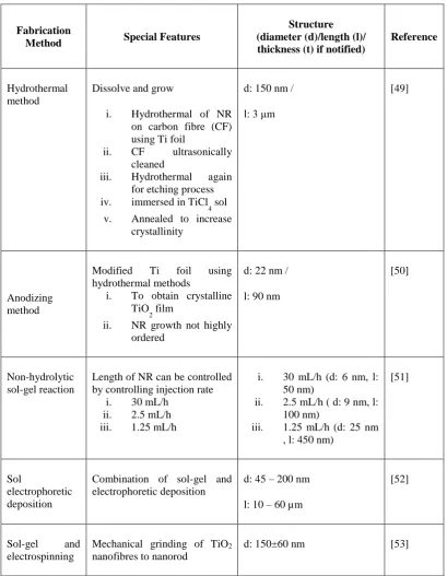
Table 2.1: Comparison of the method used to grow TiO2 nanorods
Fabrication
Method Special Features
Structure (diameter (d)/length (l)/ thickness (t) if notified)
Reference
Hydrothermal method
Dissolve and grow
i. Hydrothermal of NR on carbon fibre (CF) using Ti foil
ii. CF ultrasonically cleaned
iii. Hydrothermal again for etching process iv. immersed in TiCl
4 sol v. Annealed to increase
crystallinity
d: 150 nm /
l: 3 μm
[49]
Anodizing method
Modified Ti foil using hydrothermal methods
i. To obtain crystalline TiO
2 film
ii. NR growth not highly ordered
d: 22 nm /
l: 90 nm
[50]
Non-hydrolytic sol-gel reaction
Length of NR can be controlled by controlling injection rate
i. 30 mL/h ii. 2.5 mL/h iii. 1.25 mL/h
i. 30 mL/h (d: 6 nm, l: 50 nm)
ii. 2.5 mL/h ( d: 9 nm, l: 100 nm)
iii. 1.25 mL/h (d: 25 nm , l: 450 nm)
[51]
Sol
electrophoretic deposition
Combination of sol-gel and electrophoretic deposition
d: 45 – 200 nm
l: 10 – 60 µm
[52]
Sol-gel and electrospinning
Mechanical grinding of TiO2 nanofibres to nanorod
d: 150±60 nm [53]
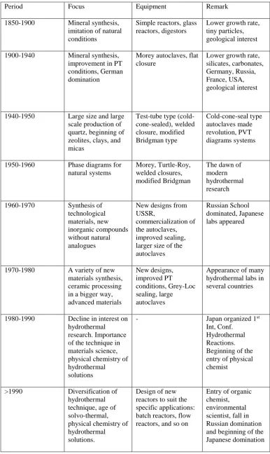
2.3 Hydrothermal
non-traditional way to obtain nanocrystalline inorganic material. In a self-explanatory word, “hydro” means water, and “thermal” means heat. According to Laudise, hydrothermal growth means growth from aqueous solution at ambient or non-ambient solution. Rabenau defined hydrothermal synthesis as the heterogeneous reactions in aqueous media above 100°C and 1 bar. Roy declares that hydrothermal synthesis involves water as a catalyst and occasionally as a component of solid phases in the synthesis at elevated temperature (>100°C) and pressure greater that a few atmospheres. Byrappa defines hydrothermal synthesis as any heterogeneous reaction in an aqueous media carried out above room temperature at a pressure greater than 1 atm. Yoshimura proposed the following definitions: reactions occurring under the conditions of high-temperature-high-pressure (>100°C, >1 atm) in aqueous in a closed system [30].
From all researchers mentioned above, it shows that hydrothermal method is one of the best methods for material synthesis at low temperature with high pressure in a closed system. By adjusting reactions conditions, many forms of ceramic materials can be synthesized such as fibre, powder, single crystals, nanoparticles, and thin films. This method also allows regulation of rate and uniformity of the nucleation, growth and aging process, which leads to improved size and morphology control.
2.3.1 History of hydrothermal
Table 2.2: Evolution of hydrothermal technology with time
Period Focus Equipment Remark
1850-1900 Mineral synthesis, imitation of natural conditions
Simple reactors, glass reactors, digestors
Lower growth rate, tiny particles, geological interest
1900-1940 Mineral synthesis, improvement in PT conditions, German domination
Morey autoclaves, flat closure
Lower growth rate, silicates, carbonates, Germany, Russia, France, USA, geological interest
1940-1950 Large size and large scale production of quartz, beginning of zeolites, clays, and micas
Test-tube type (cold-cone-sealed), welded closure, modified Bridgman type Cold-cone-seal type autoclaves made revolution, PVT diagrams systems
1950-1960 Phase diagrams for natural systems
Morey, Turtle-Roy, welded closures, modified Bridgman
The dawn of modern hydrothermal research
1960-1970 Synthesis of technological materials, new inorganic compounds without natural analogues
New designs from USSR,
commercialization of the autoclaves, improved sealing, larger size of the autoclaves
Russian School dominated, Japanese labs appeared
1970-1980 A variety of new materials synthesis, ceramic processing in a bigger way, advanced materials New designs, improved PT conditions, Grey-Loc sealing, large autoclaves
Appearance of many hydrothermal labs in several countries
1980-1990 Decline in interest on hydrothermal research. Importance of the technique in materials science, physical chemistry of hydrothermal solutions
- Japan organized 1st
Int, Conf. Hydrothermal Reactions. Beginning of the entry of physical chemist
>1990 Diversification of hydrothermal technique, age of solvo-thermal, physical chemistry of hydrothermal solutions.
Design of new reactors to suit the specific applications: batch reactors, flow reactors, and so on
Hydrothermal synthesis is a non-conventional method of synthesizing nanocrystalline inorganic materials. The synthesis method use solubility in water of almost all inorganic substances at elevated temperature and pressure, performed in an apparatus consisting of a steel pressure vessel called an autoclave. These autoclaves are usually thick-walled steel cylinders with a tight seal which ought to withstand high temperature and pressure for prolonged times span. Furthermore, the autoclave material must be inert with the respect to the solvent. The autoclave closure is the most important element. Many designs have been progressed for seals, which the most famous being the Bridgman seal. To prevent corrosion of the internal cavity the autoclave, preservative inserts are generally used. Insert may be made of carbon-free iron, silver, gold, platinum, glass, or Teflon. In this research, the insert used is Teflon. Hydrothermal method is widely used for the production of small particles in the ceramics industry.
2.3.2 Fabrication of TiO2 nanorods array using hydrothermal method
Nanostructured TiO2 was synthesized by using hydrothermal processing of titanium
alkoxides, such as Titanium Isopropoxide (TTIP) and Titanium Butoxide (TBOT). It has been widely studied and investigated as a photocatalyst and in dye-sensitize solar cell (DSSC). The morphology of the nanorods can be easily adjusted with different surfactants [55] or by changing the solvent compositions [56]. The hydrothermal method is widely used due to its simple processing, fast reaction velocity, and low cost [57]. At relatively lower temperature (~150°) a high degree of crystallinity thin film can be obtained; it also offers a uniform composition, and control over the shape and the size of particles. The hydrolysis reaction between H2O and TBOT are
schematically given as [58]:
Ti(C4H9O)4 + 4H2O Ti (OH)4 + 4C4H9OH (2.1)
Ti from the hydrolysis will then be used as a starting material for nucleation of TiO2
2Ti + 6HCl [ Ti3+] + 3H
2 (g) (2.3)
[Ti3+] + H2O TiOH2+ + H+ (2.4)
TiOH2+ + O2- Ti (IV) + O2- TiO2 (2.5)
Ti species from TBOT precursor initially starts to react with H+ ions from concentrated acidic solution. It is known that Ti3+ are not stable in aqueous solution, thus it undergoes hydrolysis with H2O to form TiOH2+. It is then oxidized to Ti (IV)
by reaction with dissolved oxygen. The Ti (IV) complex ions are thus used as the growth unit. The by-product from the reaction does not influence the sample as the sample was first rinsed with DI water before used.
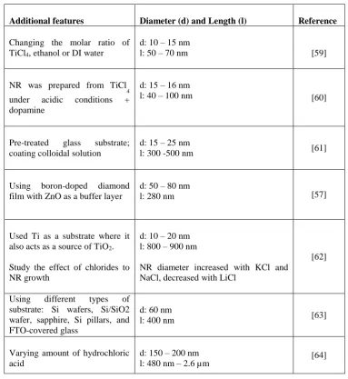
Yawen Wang et al. reported that the synthesis of pure rutile nanorods is by hydrolysis of TiCl4 ethanolic solution in water at 50°C [59]. By simply changing the
molar ratio of TiCl4, ethanol or DI water, the assembly of rutile nanorods can be
changed to flower and urchin-like morphologies. By playing around with the amount of ethanol and TiCl4 used, the resulting rods seems becoming more complex with
increasing amount of the solution. They also studied the effect of H+, Cl-, and ethanol on the morphologies by replacing TiCl4 with TTIP and adding some additives such
as KCl, HNO3, and H2SO4. It can be concluded that the strong acidic condition from
H+ and Cl- was crucial for the formation of rutile TiO2 and ethanol is needed for the
formation of rutile TiO2 in the absence of seed nanocrystal or organic surfactant
additives. Nanorods produced were of 10-15 nm in diameter and 50-70 nm in length. Doubling both amount TiCl4 and ethanol gives diameter of the nanorods 4-7 nm
while the length increased to 80-100 nm. When only the amount of TiCl4 increase,
the nanorods agglomerates to well-defined spheres with 200-600 nm in sizes.
Muhammad N. Tahir et al reported on the synthesis of in situ surface-functionalized, monocrystalline rutile TiO2 nanorods using a hydrothermal method
[60]. The rutile TiO2 nanorods were prepared from TiCl4 in aqueous solution under
acidic conditions in the presence of dopamine and are in this study, they use 3-hydroxytyramine. With this amine group functionality on its surface, it offers an excellent prospect for TiO2 nanobiocomposites and biotracers.
Large-scale, well aligned single crystalline TiO2 on pre-treated glass substrate
by hydrothermal method was prepared by Yuxiang Li et al [61]. The results demonstrated that the TiO2 was well-aligned and grown along [001] direction with
pre-treatment of the substrate is done by coating the colloidal solution prepared onto the clean glass substrate. It has been shown that the nanorods grown on coated glass substrate has better growth orientation and uniform density.
Another hydrothermal synthesis is done by Yuan et al. on boron-doped diamond film with zinc oxide (ZnO) buffer layer [57]. It is shown that the ZnO buffer layer plays an important role in increasing the density and improving the morphologies of the TiO2 nanorods. The ZnO buffer layer was so thin that it was not
detected on XRD and some of the ZnO nanoparticles may be removed in the hydrothermal process.
Lingqing Dong et al. fabricated rutile TiO2 nanorods film on titanium
substrate via a hydrothermal method [62]. They used Tetra-n-butyl titanate as the source of Ti in the presence of hydrochloric acid. The Ti substrate did not only act as a substrate but also as the source of TiO2. The nanorods thin film automatically
formed even in the absence of a precursor when the rhickness of the TiO2 reached
certain level. They also studied on the influence of metal chlorides on TiO2 nanorods
growth where chlorides such as LiCl, NaCl, and KCl were added into the mother solution. These chlorides affect the diameter and density of the nanorods by decreasing it when LiCl is added and increasing it in the presence of KCl and NaCl.
Hong En-Wang et al. used the hydrothermal method to prepare single-crystalline TiO2 nanorods [63]. The average diameter and length of nanorods
prepared are 60 nm and 400 nm respectively. They stated that this method shows great versatility and can be used to grow TiO2 nanorods on large diversity of
substrate including Si, Si/SnO2, sapphire, and fluorine-doped tin oxide (FTO).
S. Venkatachalam et al. also used hydrothermal treatment to produce TiO2
comparison of hydrothermal technique used to fabricate TiO2 nanorods array is
[image:36.595.130.514.191.609.2]summarised in Table 2.3.
Table 2.3: Comparison of hydrothermal technique used to fabricate TiO2 nanorods
array
Additional features Diameter (d) and Length (l) Reference
Changing the molar ratio of TiCl4, ethanol or DI water
d: 10 – 15 nm
l: 50 – 70 nm [59]
NR was prepared from TiCl 4 under acidic conditions + dopamine
d: 15 – 16 nm
l: 40 – 100 nm [60]
Pre-treated glass substrate; coating colloidal solution
d: 15 – 25 nm
l: 300 -500 nm [61]
Using boron-doped diamond film with ZnO as a buffer layer
d: 50 – 80 nm
l: 280 nm [57]
Used Ti as a substrate where it also acts as a source of TiO2.
Study the effect of chlorides to NR growth
d: 10 – 20 nm l: 800 – 900 nm
NR diameter increased with KCl and NaCl, decreased with LiCl
[62]
Using different types of substrate: Si wafers, Si/SiO2 wafer, sapphire, Si pillars, and FTO-covered glass
d: 60 nm
l: 400 nm [63]
Varying amount of hydrochloric acid
d: 150 – 200 nm
l: 480 nm – 2.6 µm [64]
2.4 Ultraviolet Sensor
caused several problems. First, Si has a low bandgap, which is 1.1eV; causing low responsivity towards ultraviolet radiation and requiring a visible light filter if applied in the device structure [69]. Si is also not suitable to be used as it has limitation in harsh environmental conditions, for example UV detection at high temperature [70]. Meanwhile, GaN, SiC, and diamond shows a decent performance under high temperature conditions. However, the materials are not cost effective as they have high fabrication cost making it not fitting for large scale production [71].
2.4.1 Ultraviolet sensor using titanium dioxide nanomaterials
A number of materials, including TiO2 nanostuructured have been proposed
and studied intensively in order to fabricate a UV sensor with good stability and reliability at a reasonable prices. Among the TiO2 nanomaterials that have been used
for UV detectors are TiO2 nanoflowers. For an example of fabrication of TiO2
nanoflowers UV photoconductive sensors, the work by Xihong Zu et al. has been referred [72]. By using combined method of hydrothermal and in-situ multiple wet chemical depositions method, the successfully constructed structure was composed of heterostructured arrays of TiO2 nanowires (NWs) and polyaniline nanoflowers
(PANI NFs) in sandwiches form. With comparison to 254 nm, the resulting photodetector exhibits excellent UV sensitivity and fast response speed with UV illumination at 365 nm wavelength.
Another work by Huan Wang et al. also used the same structure of sandwiches layer of TiO2 and PANI [73]. But this time, the TiO2 are nanorods
(TNRs) structure and the PANI layer are nanowires (PANI NWs). The fabrication method used for PANI NWs was the chemical oxidation method meanwhile TNRs are synthesized using hydrothermal method. This work has also been tested using two UV wavelengths that are 254 and 365 nm. The 365 nm UV photocurrent of the designed UV photodetector was as high as 3.5 x 10⁻⁴ A, and 254 nm UV photocurrent was only 0.16 x 10⁻⁴ A. This study can provide opportunities for developing devices
that can recognize different wavelengths of UV light.
W. F. Xiang et al. fabricated two types of nanocrystalline TiO2 films; porous
solution [74]. They used two colloidal silver electrodes as top electrode for TiO2
surface and bottom electrodes for FTO separated by about 3 mm. The rise time and decay time of the P-detector and D-detector are 19 and 136 ns, and 14 and 100 ns, respectively. By comparing these two types of detector, P-detector is found to give higher responsivity due to a light scattering effect.
Another solution-based technique that is spray pyrolysis deposition (SPD) is used by Masayuki Okuya et al for UV sensor application [75]. The measurement was carried out under the light intensity of 20 μW/cm2 irradiated directly on the sensors.
The fabrication process varied the solvent used among ethanol, propanol, and 2-butanol in which the results showed that ethanol gives the higher intensity from photo response of UV sensors. The UV response of the photodiode became more sensitive with increasing porosity of TiO2 layer deposited from ethanol solution.
Sensitivity of the UV sensor can be improved in this study by doping a little amount of aluminium to reduce the depletion layer. The photo response of TiO2 UV sensor
fabricated with aluminium layer showed higher intensity than that fabricated without aluminium layer.
An ultraviolet sensor based on TiO2 nanorods that are grown on a p-type
substrate seeded with a TiO2 layer and synthesized by radio frequency reactive
magnetron sputtering was done by Abbas M. Selman et al [76]. The TiO2 nanorods
were grown by using chemical bath deposition (CBD) method. The device showed 3.79 x 10² sensitivity when it was exposed to 325 nm light at 5V bias voltage.
2.4.2 Ultraviolet sensor mechanism
The enhancement of TiO2 conductivity during dark and UV illumination can be
explained as follows [77]. Both intrinsic conductivity and the conductivity of TiO2 in
the dark can be described by equation 2.4:
Where σ is the conductivity, e is the electronic charge, n is the charge carrier density, and μ is the carrier mobility. Under a bias voltage across the metal contact gap, the current density, J, can be found by equation 2.5:
J = σF
whereF = V / x
(2.5)Here, F is the applied electric field, V is the bias voltage, and x is the distance. Under UV illumination, a change in photoconductivity, Δσ, occurs either by a change in the carrier concentration, Δn, or by a change in the carrier mobility, Δμ, as indicated by the equation 2.6:
Δσ = σ
light– σ
dark= e (μΔn + nΔμ)
(2.6)Generally, the photocurrent density, Jphotocurrent, can be expressed as a function of time by equation 2.7:
J
photocurrent= [μ(t)Δn(t) + n(t)Δμ(t)] eF
(2.7)In many semiconductors, the change in mobility can be entirely neglected because Δn>>Δμ; therefore, the equation can be simplified as equation 2.8:
J
photocurrent= ΔσF
From this equation, it can be concluded that the photoconductivity of TiO2
UV sensor depends on the mobility, carrier concentration, and the electric field or the bias voltage. Thus, to increase the photocurrent of the device, these three parameters must be improved. For example, the mobility of TiO2 can be enhanced by using
highly crystalline TiO2 nanostructures such as nanowires or nanorods. Additionally,
the carrier concentration of TiO2 can be increased by the doping process.
According to the previous study, the photoconduction of UV sensor is governed by oxygen adsorption and desorption on its surface, as shown in Figure 2.2 [78]. This mechanism is widely accepted as the cause of high photocurrent values under UV illumination as the lifetime of the photoexcited electron is increased. According to this mechanism, surrounding oxygen molecules can be adsorbed onto the nanorods surface by capturing the free electrons from the TiO2 nanostructure, as
shown in 2.9:
O
2+ e
- O
2- (2.9)Where O2 is the oxygen molecule, e- is a free electron, and O2- is adsorbed
oxygen on the nanorod surface. This process is illustrated by Process 1 in Figure 2.2. The adsorption of oxygen onto the surface causes bend bending. When UV light is incident on the surface of the nanostructure, electron-hole pairs are generated according to the following equation 2.10:
hv h
++ e
-(2.10)
Where hv is the photon energy from the UV light, h is a plank’s constant, v is
the photon frequency, h+ is a photogenerated hole in the valence band, and e- is the
photogenerated electron in the conduction band. Large surface area is needed as it facilitates fast surface reaction as the photogenerated hole reacts with negatively charged adsorbed oxygen, as shown by equation 2.11:
This process releases oxygen molecules from the nanorods surface as shown by Process 2 in Figure 2.2. This will cause hole trapping phenomenon at the TiO2
surface, as illustrated by Process 3 and Process 4, and leaves behind the electron of the pair, as indicated by Process 5 and Process 6, which results in increasing of the conductivity of the nanostructures. The unpaired e- will either collected at the metal contact or recombine with the holes when the oxygen is re-adsorbed on the TiO2
surfaces, as shown by Process 7 in Figure 2.2. The maximum photocurrent can be achieved when the generation rate of the electron-hole pairs and recombination is equivalent. When illumination is removed, the oxygen molecule recombines with the electron, leading to the decrease in film conductivity.
O2 - O2 - O2 - O2 - O2 - O2 O2 - O2 - O2 - E E Surface trap state due to adsorbed oxygen Process 1 E
O2-
O2-
O2 - O2 - O2 O2 O2 O2 E Process 6 Process 4 Process 2 Process 3 Process 5 UV Illumination Process 7
In the dark Under UV illumination
Legends: : electron : hole
O : adsorbed oxygen
O
2
: oxygen molecule
EC : conduction band
[image:41.595.120.523.332.659.2]EV : valence band
Figure 2.2: The mechanism of photoconduction in TiO2-based UV sensor under both
CHAPTER 3
METHODOLOGY
3.1 Introduction
In this chapter, preparation of the titanium dioxide (TiO2) nanorods using
hydrothermal synthesis is presented. Three main topics will be explained in this chapter including substrate cleaning, preparation of the TiO2 solutions for nanorods
array using hydrothermal methods, and the characterisation methods including surface morphology study, chemical composition, electrical, and optical properties. The experimental details are given in the subsequent chapter. Figure 3.1 shows the flow chart for nanostructured TiO2 thin film preparation and characterization.
FTO substrate cleaning
Fabrication of TiO2 nanorods thin film using
hydrothermal method
Characterization method: FESEM, XRD, Raman spectra, UV-Vis-NIR, IV measurement (2-point probe),
[image:42.595.250.388.546.718.2]photocurrent measurement
Figure 3.1: Summarized of nanostructured TiO2 thin film
3.2 Substrate cleaning by sonicating method
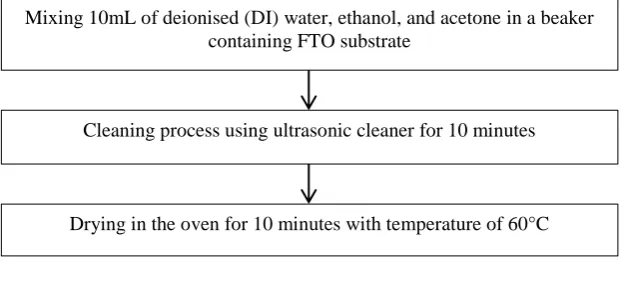
Before the fabrications, substrate used, that is fluorine-doped tin oxide (FTO) was cleaned in order to remove contaminants. The contaminations on the FTO might affect the material growth, thus affecting the properties of the material. FTO substrate is a substrate that is transparent, low cost, has high-temperature resistant, and chemically inert. Also, FTO substrate exhibit electrical conductivity and at the same time allows transmission of solar cell radiation on its active region[79]. The substrate cleaning procedure is summarized in Figure 3.2.
3.3 Preparation of TiO2 solution for hydrothermal reaction
The TiO2 hydrothermal were prepared by using titanium butoxide (TBOT) as a
precursor (starting material), hydrochloric acid (HCl) as a chelating agent, and deionised water (DI) as a solvent. Chelating agent is ligand that can form bonds (covalent bondings) at more than one point. It is a substances whose molecules can form a several bonds to a single metal ion. Meanwhile, deionised water acts as a function of adding the oxygen (O2) element into TBOT for hydrolysis process. 120
mL of concentrated hydrochloric acid (HCl) (36.5 % ~ 38 %) was dissolved in 120 mL of DI water as chemical solution for hydrothermal process. The mixture was vigorously stirred for 5 minutes on the hot plate stirrer and then TBOT was added drop wise using a capillary tube. After stirring for nearly 15 minutes, the solution was put into steel made autoclave with Teflon made liner (300 mL) for hydrothermal process in which the FTO glass substrate were put with the conducting FTO surface
Mixing 10mL of deionised (DI) water, ethanol, and acetone in a beaker containing FTO substrate
Cleaning process using ultrasonic cleaner for 10 minutes
[image:43.595.163.474.305.446.2]Drying in the oven for 10 minutes with temperature of 60°C
facing the walls of the Teflon. Nucleation of TiO2 seed in the solution leads to the
growth of nanoflowers [80,81]. The conductive side of the FTO was put facing the wall to avoid deposition of nanoflowers on top of the nanorods. The autoclave steel used was shown in Figure 3.3. The process was performed at 150°C with a variation of reaction time, volume of TBOT, and volume of hydrochloric acid used. After that, the autoclave was taken out from oven and cooled down in room temperature for 5 hours to allow the steel made autoclave to cool and touchable. The prepared samples were rinsed with DI water and left to dry at room temperature. Figure 3.4 shows the FTO substrate before and after the hydothermal reaction. Summarised step for preparing the solution is shown in Figure 3.5 and the details experimental parameters are tabulated in Table 3.1.
Table 3.1: Preparation of TiO2 solution for hydrothermal reaction
Solution
preparation Materials
Precursor Titanium butoxide
Chelating agent Hydrochloric acid
Solvent DI water
Solution volume 240 mL
Fabrication
Process Hydrothermal Temperature 150 °C
Autoclave
[image:44.595.117.513.409.694.2]Teflon
Figure 3.3: Autoclave used for hydrothermal process
Solution
REFERENCE
[1] M. C. Mathpal, A. K. Tripathi, M. K. Singh, S. P. Gairola, S. N. Pandey, and A. Agarwal, “Effect of annealing temperature on Raman spectra of TiO2
nanoparticles,” Chem. Phys. Lett., vol. 555, pp. 182–186, 2013.
[2] W. Zhou, X. Liu, J. Cui, D. Liu, J. Li, H. Jiang, J. Wang, and H. Liu, “Control synthesis of rutile TiO2 microspheres, nanoflowers, nanotrees and nanobelts via acid-hydrothermal method and their optical properties,” CrystEngComm, vol. 13, no. 14, pp. 4557–4565, 2011.
[3] A. C. Arias, J. D. MacKenzie, I. McCulloch, J. Rivnay, and A. Salleo, “Materials and applications for large area electronics: Solution-based approaches,” Chem. Rev., vol. 110, no. 1, pp. 3–24, 2010.
[4] Y. Liao, W. Que, Q. Jia, Y. He, J. Zhang, and P. Zhong, “Controllable synthesis of brookite/anatase/rutile TiO2 nanocomposites and
single-crystalline rutile nanorods array,” J. Mater. Chem., vol. 22, no. 16, pp. 7937– 7944, 2012.
[5] X. Feng, K. Shankar, O. K. Varghese, M. Paulose, T. J. Latempa, and C. a Grimes, “Vertically aligned single crystal TiO2 nanowire arrays grown
directly on transparent conducting oxide coated glass: synthesis details and applications.,” Nano Lett., vol. 8, no. 11, pp. 3781–3786, 2008.
[6] E. Hendry, M. Koeberg, B. O’Regan, and M. Bonn, “Local Field Effects on Electron Transport in Nanostructured TiO2 Revealed by Terahertz
Spectroscopy,” Nano Lett., vol. 6, no. 4, pp. 755–759, 2006.
[7] E. Hosono, S. Fujihara, K. Kakiuchi, and H. Imai, “Growth of Submicrometer-Scale Rectangular Parallelepiped Rutile TiO2 Films in Aqueous TiCl3
Solutions under Hydrothermal Conditions,” J. Am. Chem. Soc., vol. 126, no. 25, pp. 7790–7791, 2004.
[8] M. Kosmulski, “The significance of the difference in the point of zero charge between rutile and anatase,” Adv. Colloid Interface Sci., vol. 99, no. 3, pp. 255–264, 2002.
[9] T. Koutchma, “Basic Principles of UV Light Generation,” in Food Plant Safety, First., Elsevier, 2014, pp. 3–13.
[10] T. Koutchma, “UV Safety,” in Preservation and Shelf Life Extension, First., Elsevier, 2014, p. 59.
[11] T. Koutchma, “Fundamentals of UV Light Emission, Transmission, and Absorption,” Preserv. Shelf Life Ext., pp. 1–3, 2014.
2006.
[13] O. Ola and M. M. Maroto-Valer, “Review of material design and reactor engineering on TiO2 photocatalysis for CO2 reduction,” J. Photochem. Photobiol. C Photochem. Rev., vol. 24, pp. 16–42, Sep. 2015.
[14] R. Edy, Y. Zhao, G. S. Huang, J. J. Shi, J. Zhang, A. A. Solovev, and Y. Mei, “TiO2 nanosheets synthesized by atomic layer deposition for photocatalysis,” Prog. Nat. Sci. Mater. Int., vol. 26, no. 5, pp. 493–497, Oct. 2016.
[15] J. Xiong, B. Yang, J. Yuan, L. Fan, X. Hu, H. Xie, L. Lyu, R. Cui, Y. Zou, C. Zhou, D. Niu, Y. Gao, and J. Yang, “Efficient organic photovoltaics using solution-processed, annealing-free TiO2 nanocrystalline particles as an
interface modification layer,” Org. Electron., vol. 17, pp. 253–261, 2015. [16] P. H. Falla, M. O. G. Dias, H. Vieira, R. da S. P. Junior, L. H. X. da Silva, and
P. H. O. Nogueira, “Optimization the Efficiency Photovoltaic Solar Cells Using Synthesized TiO2 Semiconductor Nanomaterials and Functionalized
Carbon Nanotubes.,” Energy Procedia, vol. 57, pp. 1860–1867, 2014.
[17] Y.-M. Sung, “Deposition of TiO2 Blocking Layers of Photovoltaic Cell Using
RF Magnetron Sputtering Technology,” Energy Procedia, vol. 34, pp. 582– 588, 2013.
[18] M. Okuya, “Porous TiO2 thin films prepared by spray pyrolysis deposition
(SPD) technique and their application to UV sensors,” Solid State Ionics, vol. 172, no. 1–4, pp. 527–531, Aug. 2004.
[19] E. N. Bunting, “Phase equilibria in the systems TiO2, TiO2-SiO2 and TiO2
-Al2O3,” Bur. Stand. J. Res., vol. 11, no. November, 1933.
[20] M. Landmann, E. Rauls, and W. G. Schmidt, “The electronic structure and optical response of rutile, anatase and brookite TiO2.,” J. Phys. Condens. Matter, vol. 24, no. 19, p. 195503, 2012.
[21] L. Forro, D. Emin, L. Zuppiroli, D. De Physique, E. Polytechnique, F. De Lausanne, H. Berger, and E. P. F. De Lausanne, “High mobility n-type charge carriers in large single crystals,” New York, vol. 75, pp. 633–635, 1994.
[22] S. U. M. Khan, M. Al-Shahry, and W. B. Ingler, “Efficient photochemical water splitting by a chemically modified n-TiO2.,” Science (80-. )., vol. 297,
no. 5590, pp. 2243–2245, 2002.
[23] M. K. Nowotny, P. Bogdanoff, T. Dittrich, S. Fiechter, a. Fujishima, and H. Tributsch, “Observations of p-type semiconductivity in titanium dioxide at room temperature,” Mater. Lett., vol. 64, no. 8, pp. 928–930, 2010.
[25] K. M. Glassford and J. R. Chelikowsky, “Structural and Electronic-Properties of Titanium-Dioxide,” Physical Review B, vol. 46, no. 3. pp. 1284–1298, 1992.
[26] T.-D. Nguyen Phan, H.-D. Pham, T. Viet Cuong, E. Jung Kim, S. Kim, and E. Woo Shin, “A simple hydrothermal preparation of TiO2 nanomaterials using
concentrated hydrochloric acid,” J. Cryst. Growth, vol. 312, no. 1, pp. 79–85, Dec. 2009.
[27] H. Yang, S. Zhu, and N. Pan, “Studying the mechanisms of titanium dioxide as ultraviolet-blocking additive for films and fabrics by an improved scheme,”
J. Appl. Polym. Sci., vol. 92, no. 5, pp. 3201–3210, 2004.
[28] Y. Li, X. Lv, and J. Li, “High performance binderless TiO2 nanowire arrays
electrode for lithium-ion battery,” Appl. Phys. Lett., vol. 95, no. 11, pp. 2009– 2011, 2009.
[29] X. D. Tang, M. Chen, M. A. Joiner, N. Brot, H. Weissbach, S. H. Heinemann, J. Lykkesfeldt, C. M. Wehr, R. T. Ingersoll, J. C. Bartholomew, B. N. Ames, A. G. Pletnev, R. Putnak, and J. Speicher, “Study of Nd3+,Pd2+,Pt4+, and Fe3+
dopant effect on photoreactivity of TiO2 nanoparticles,” J. Biochem., vol. 99, no. 10, 2002.
[30] K. Byrappa and M. Yoshimura, Handbook of Hydrothermal Technology, 2001st ed. New York: William Andrew Publishing, 2001.
[31] R. Cherrington, D. J. Hughes, S. Senthilarasu, and V. Goodship, “Inkjet-Printed TiO2 Nanoparticles from Aqueous Solutions for Dye-Sensitized Solar
Cells (DSSCs),” Energy Technol., vol. 3, no. 8, pp. 866–870, 2015.
[32] R. Govindaraj, S. M. Pandian, P. Ramasamy, and S. Mukhopadhyay, “Sol-gel synthesized mesoporous anatase titanium dioxide nanoparticles for dye sensitized solar cell (DSSC) applications,” Bull. Mater. Sci., vol. 38, no. 2, pp. 291–296, 2015.
[33] S. K. Prakash, H. Singh, H. Panjiar, S. Manhas, and B. S. S. Daniel, “Application of Graphene Oxide and TiO2 in the fabrication of Dye sensitized
solar cells module by electrode modification,” Adv. Mater. Process. Challenges Oppor., vol. 585, pp. 255–259, 2012.
[34] X. Chen and S. S. Mao, “Titanium Dioxide Nanomaterials : Synthesis , Properties , Modifications , and Applications,” Chem. Rev., vol. 107, pp. 2891–2959, 2007.
[35] G. Peng, Y. Zhou, Y. He, X. Yu, X. a Zhang, G. Y. Li, and H. Haick, “UV-induced SiC nanowire sensors,” J. Phys. D. Appl. Phys., vol. 48, no. 5, p. 55102, 2015.
![Figure 1.2: The primitive cell unit for rutile TiO2 [19]](https://thumb-us.123doks.com/thumbv2/123dok_us/8756430.892984/23.595.192.447.566.743/figure-primitive-cell-unit-rutile-tio.webp)
![Figure 1.3: Schematic illustration of the formation mechanisms of the anatase and rutile crystal phase [26]](https://thumb-us.123doks.com/thumbv2/123dok_us/8756430.892984/24.595.138.506.112.343/figure-schematic-illustration-formation-mechanisms-anatase-rutile-crystal.webp)
![Figure 2.1: TiO2 nanorods fabricated by (a) sol electrophoretic [52] and (b) sol-gel](https://thumb-us.123doks.com/thumbv2/123dok_us/8756430.892984/29.595.133.503.560.711/figure-tio-nanorods-fabricated-sol-electrophoretic-sol-gel.webp)