Technology (IJRASET)
Analysis of Switched Boost Inverter for Induction
Machine Drive Application
Abstract—Recently, developments in power electronics and semiconductor technology have lead improvements in power electronic systems. The Switched Boost Inverter is a single stage dc-ac converter, whose output voltage can be either greater or less than its input dc voltage. This converter can offer both dc and ac loads, simultaneously. Also, this converter allows shoot-through of the inverter legs without causing any damage to the converter. In this paper, the principle of operation of the Switched Boost Inverter is explained. Also, a Pulse Width Modulation (PWM) control strategy for the Switched Boost Inverter is formulated and implemented using a simple analog circuit. These inverters use a unique impedance network, united between the power source and converter circuit, to offer both voltage buck and boost properties, which cannot be obtained by conventional voltage-source and current-source inverters. In this work the switched boost inverter is applied to induction machine drive. The simulations results are obtained by MATLAB/SIMULINK software.
Key words-- Pulse Width Modulation (PWM), voltage source inverter (VSI), Switched Boost Inverter.
I. INTRODUCTION
The developments in power electronics and semiconductor technology have lead improvements in power electronic systems. Hence, various circuit configurations namely switched type inverters have became popular and considerable interest by researcher are given on them [1]-[3]. Nowadays, ac motor drives are widely used in electromechanical energy conversion systems. Modern power electronic inverters are based on PWM techniques with switches characterized by very small switching times. As a result, the motor windings are subjected to a very large amount of HF voltage components. With the improvement of advanced power electronic switching devices, the high-frequency switching operation [4] has been enabled, and the operation of pulse width modulation (PWM) inverters for driving induction motors has been improved. The dv/dt filters, common-mode filters, and pulse width-modulation (PWM) techniques have been proposed to mitigate the aforementioned problems [5–7]. However, for longer life of the motor, it is always required to operate the machine with sinusoidal voltages with front end DC/AC switched converters for residential applications. Generally, current controlled voltage source inverters are used to interface the intermittent RES in distributed system. The Z-Source inverter is a new and attractive topology for the power electronics interface.
Fig.1 Single-phase full bridge Z-Source inverter
The DC-side of a conventional single-phase full bridge voltage source inverter is modified with a unique X-shape impedance network, which is named as the Z-Source network. Therefore, shoot-through state, which is forbidden in conventional voltage source inverters, is allowed and implemented here for voltage boosting. Because the capacitor in the Z-Source network may be charged to a higher voltage than the DC source, a diode is connected to control the possible discharging. To realize the bidirectional power flow characteristic, the diode can be substitute with an IGBT with anti-paralleled diode to form a bidirectional Z-Source converter.
B.Apurupa1, D.T.Ramya Sai2, D.Harish3
Department of Electrical & Electronics Engineering,
high step-up voltage gain dc-dc converter is required to adjust the voltage of the dc – dc interface. The traditional Boost converters cannot provide a high dc voltage gain, even for an excessive duty cycle. It also may results in serious reverse –recovery problems and increases the rating of all devices. This paper presents a novel power converter called switched boost inverter (SBI) which works similarly to a ZSI. This converter uses more active components and lower number of inductors and capacitors compared to the original ZSI while retaining its operational advantages. As a result, the conversion efficiency is degraded and the electromagnetic interference (EMI) problem is severe under this situation [7]-[9].
[image:3.612.203.414.199.352.2]II. SWITCHED BOOST INVERTER
Fig.2 Circuit diagram of SBI topology
Fig. 2 shows the schematic of the SBI in which a switched boost network comprising of one active switch (S), two diodes (Da, Db), one inductor (L), and one capacitor (C) is connected between voltage source Vg and the inverter bridge. A low-pass LC filter is used at the output of the inverter bridge to filter the switching frequency components in the inverter output voltage VAB. Similar to a ZSI, the SBI also utilizes the shoot-through state of the H-bridge inverter means, both switches in one leg of the inverter are turned on simultaneously to boost the input voltage Vg to VC [10].
To explain the steady state operation of the SBI, assume that the inverter bridge is in shoot through state for interval D.Ts in a switching cycle Ts.
Fig. 3 Equivalent circuit of SBI during D.TS interval
[image:3.612.215.392.461.640.2]Technology (IJRASET)
Fig.4 Equivalent circuit of SBI during (1 − D).TS interval
The inverter bridge is represented by a current source in this interval as shown in the Fig.4. Now the voltage source and inductor together supply power to the inverter and the capacitor through diodes Da and Db. The inductor current in this duration equals the capacitor charging current added to the inverter input current. Note that the inductor current is assumed to be sufficient enough for the continuous conduction of diodes Da and Db for the interval (1− D) Ts [11].
III. PWM CONTROL OF SBI
The SBI utilizes the shoot-through state of VSI to boost the input voltage Vg, whereas the traditional PWM techniques of VSI do not permit the inverter bridge to be in shoot-through state. This section describes two different PWM techniques suitable for SBI.
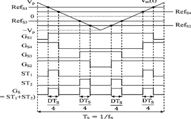
[image:4.612.212.400.330.447.2]Fig. 5 Generation of control signals for SBI using traditional PWM technique of ZSI
Fig. 5 shows the gate control signals for SBI obtained using the traditional PWM technique of ZSI. In this scheme, the gate control signals GSX (x = 1 to 4) are generated by comparing the reference signals Ref SX (x = 1 to 4) with a triangular carrier signal Vtri(t) of amplitude Vp. The signal GSX becomes high whenever the value of the corresponding reference signal becomes either higher or lower than that of the carrier. The gate control signal (GS) for switch S is obtained by adding the two individual shoot-through periods ST1 and ST2 as shown in the figure.
Note that the switch S has four switching cycles in a time period Ts which leads to high switching losses.
[image:4.612.210.387.557.650.2]Fig.6 Schematic of the modified PWM control circuit
VI. SIMULATION RESULTS
Here the simulation results carried out by two cases. 1) Proposed Switched Boost Inverter 2) SBI with Induction Machine Drive Application.
CASE-1 Proposed Switched Boost Inverter
The below figures shows the MATLAB/SIMULINK results of the proposed system, the below figure shows the MATLAB/SIMULINK circuit of the proposed system
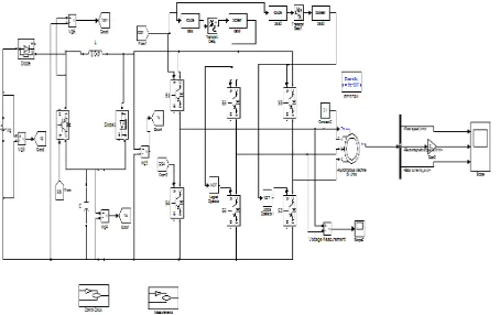
[image:5.612.201.413.195.301.2]Fig. 7 Matlab/simulink model of switched boost inverter
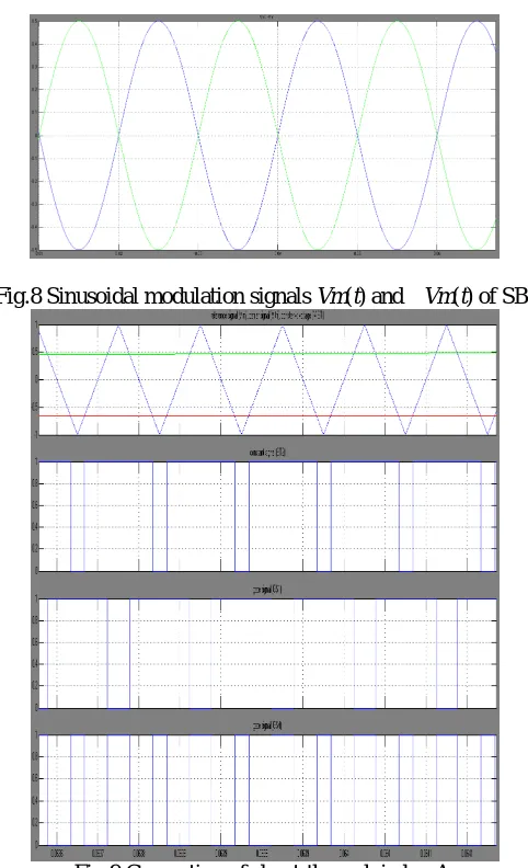
Fig.8 Sinusoidal modulation signals Vm(t) and −Vm(t) of SBI
[image:5.612.185.426.323.719.2]Technology (IJRASET)
Fig.10 Generation of shoot-through in leg B
Fig.12 Steady-state operation of the SBI Input voltage (Vg), capacitor voltage (VC), output voltage of H-bridge (VAB), and load voltage (VO)
Technology (IJRASET)
Fig.14 FFT analysis of inverter output voltage is 36.51%
Case 2: SBI with Induction Machine Drive Application
[image:8.612.199.418.521.701.2]Induction motor has been operated as a work horse in the industry due to its low cost, easy construction, solid robustness and good efficiency. The proposed converter has been highly efficient because it recycles the energy stored in leakage inductor. Comparison of the SBI and ZSI with the same input and output parameters are observed. It exhibits properties similar to that of ZSI with lower number of passive components. This may lead to significant reduction in the size, weight, and cost of the power converter and makes it suitable for low-power applications. Total simulation results are verified by using MATLAB/SIMULINK software. THD also well within in IEEE standards.
REFERENCES
[1] J.L. Davies, M. Malengret , “Application of induction motor for solar water pumping” , AFRICON '92 Proceedings., 3rd AFRICON Conference, pp. 209 – 212, 1992.
[2] B. Kroposki, R. de Blasio, “Technologies for the new millennium: Photovoltaics as a distributed resource,” Proc. IEEE Power Eng. Soc. Summer Meeting,Vol. 3, pp. 1798–1801, 2000.
[3] Pollikas A., Implementation of distributed generation technologies in isolated power, Renewable and Sustainable Energy Reviews, Vol. 11, 2007, pp. 30-56. [4] Q. Li, and P. Wlfs, A review of single phase photovoltaic module integrated converter topologies with three different DC link configurations, IEEE Transactions on Power Electronics, Vol. 23, No. 3, May 2008, pp. 1320-1333.
[5]. M. Calais, J. Myrzik, T. Spooner, and V.G. Agelidis, Inverters for single-phase grid connected photovoltaic systems-An overview, IEEE Proceedings PESC, Vol. 4, 2002, pp. 1995-2000.
[6] J. Liu, J. Hu, and L. Xu, “Dynamic modeling and analysis of Z source converter-derivation of ac small-signal model and design-oriented analysis,” IEEE Trans. Power Electronics. vol. 22, no 5, pp. 1786–1796, Sep. 2007.
[7] R. W. Erickson and D. Maksimovic, Fundamentals of Power Electronics, 2nd ed. Norwell, MA: Kluwer, Jan. 2001.
[8] N. Mohan, T. Undeland, and W. Robbins, Power Electronics: Converters, Applications and Design, 2nd ed. New York: Wiley, 1995.
[9] P. C. Loh, D. Vilathgamuva, Y. S. Lai, G. Chua, and Y. Li, “Pulse-width modulation of Z-source inverters,” IEEE Trans. Power Electron., vol. 20, no. 6, pp. 1346–1355, Nov. 2005.
[10] Z. J. Zhou, X. Zhang, P. Xu, and W. X. Shen, “Single-phase uninterruptible power supply based on Z-source inverter,” IEEE Trans. Ind. Electron., vol. 55, no. 8, pp. 2997–3004, Aug. 2008.