PCGrade Parallel Processing and Hardware Acceleration for LargeScale Data Analysis
Original Citation
Yang, Su (2009) PCGrade Parallel Processing and Hardware Acceleration for LargeScale Data
Analysis. Doctoral thesis, University of Huddersfield.
This version is available at http://eprints.hud.ac.uk/id/eprint/8754/
The University Repository is a digital collection of the research output of the
University, available on Open Access. Copyright and Moral Rights for the items
on this site are retained by the individual author and/or other copyright owners.
Users may access full items free of charge; copies of full text items generally
can be reproduced, displayed or performed and given to third parties in any
format or medium for personal research or study, educational or notforprofit
purposes without prior permission or charge, provided:
•
The authors, title and full bibliographic details is credited in any copy;
•
A hyperlink and/or URL is included for the original metadata page; and
•
The content is not changed in any way.
For more information, including our policy and submission procedure, please
contact the Repository Team at: [email protected].
and Hardware Acceleration for
Large-Scale Data Analysis
Yang Su
A thesis submitted to the University of Huddersfield in partial
fulfilment of the requirements for the degree of Doctor of Philosophy
School of Computing and Engineering
University of Huddersfield
I
Acknowledgments
I would like to thank the School of Computing and Engineering at the University of Huddersfield for providing this great opportunity of study and facilitating me throughout this project. I wish to thank my colleagues at the Computer Graphics, Imaging and Vision (CGIV) Research Group and the Centre of Precision Technology within the University of Huddersfield for their continuous and consistent help and support to the project and myself.
First and foremost, I would like to express my sincere gratitude to my director of studies, Dr Zhijie Xu, for his exceptional support and guidance throughout the project. Having Dr Xu as an adviser has been an amazing experience. He was willing to take a chance on my research from the beginning, and has always pushed me to fill in that one last detail to elevate the level of my thinking and my work.
Great appreciation also goes to my second supervisor, professor Xiangqian Jiang, whose help and support has been of significant benefit to me during the project.
ii
Abstract
Arguably, modern graphics processing units (GPU) are the first commodity, and desktop parallel processor. Although GPU programming was originated from the interactive rendering in graphical applications such as computer games, researchers in the field of general purpose computation on GPU (GPGPU) are showing that the power, ubiquity and low cost of GPUs makes them an ideal alternative platform for high-performance computing. This has resulted in the extensive exploration in using the GPU to accelerate general-purpose computations in many engineering and mathematical domains outside of graphics. However, limited to the development complexity caused by the graphics-oriented concepts and development tools for GPU-programming, GPGPU has mainly been discussed in the academic domain so far and has not yet fully fulfilled its promises in the real world.
iii
not only a graphics device but a streaming coprocessor of CPU. Secondly, the proposed GPGPU programming framework are applied to the practical engineering applications, namely, the surface metrological data processing and image processing, to generate the programming models that aim to carry out parallel computing for the corresponding algorithms. The acceleration performance of these models are evaluated in terms of the speed-up factor and the data accuracy, which enabled the generation of quantifiable benchmarks for evaluating consumer-grade parallel processors. It shows that the GPGPU applications outperform the CPU solutions by up to 20 times without significant loss of data accuracy and any noticeable increase in source code complexity, which further validates the effectiveness of the proposed GPGPU general programming framework. Thirdly, this thesis devised methods for carrying out result visualization directly on GPU by storing processed data in local GPU memory through making use of GPU’s rendering device features to achieve real-time interactions.
iv
List of Publications
1. Yang Su, Zhijie Xu (2009) “Parallel Implementation of Wavelet-based Image Denoising on Programmable PC-grade Graphics Hardware”.
Signal Processing, ISSN: 0165-1684, In Press, Corrected Proof.
2. Yang Su, Zhijie Xu and Xiangqian Jiang (2009) “Real-time VE Signal Extraction and Denoising Using Programmable Graphics Hardware”.
International Journal of Automation and Computing, ISSN: 1476-8186, Vol.6, Issue 4, pp.326-334.
3. Yang Su, Zhijie Xu, Xiangqian Jiang and J. Pickering (2008) “Discrete Wavelet Transform on Consumer-Level Graphics Processing Unit”.
Proceedings of Computing and Engineering Annual Researchers’ Conference 2008, ISBN 978-1-86218-067-3, UK. pp. 40-47.
4. Yang Su, Zhijie Xu and Xiangqian Jiang (2008) “Stream-Based Data Filtering for Accelerating Metrological Data Characterization”.
Proceedings of the 14th International Conference on Automation & Computing, ISBN 978-0-9555293-2-0, September 2008, London. pp. 81-85.
v
List of Figures
Figure 2.1 Different stage overlap of instruction pipeline in RISC machine ... 9
Figure 2.2 Models of a MISD architecture ... 11
Figure 2.3 Models of a SIMD architecture ... 11
Figure 2.4 Models of a MIMD architecture ... 12
Figure 2.5 Abstract graphics pipeline defined in PHIGS ... 16
Figure 2.6 Abstract graphics pipeline between in 1995 and 1998 ... 18
Figure 2.7 Abstract graphics pipeline (integrated T & L) at late 1990s ... 19
Figure 2.8 The enhanced GPU capability ... 20
Figure 2.9 A 3D head rendered by vertex shader and fixed-function graphics pipeline respectively ... 21
Figure 2.10 The animation effect produced by pixel shader ... 21
Figure 2.11 Hardware abstracts of GPUs with programmable vertex and pixel shaders . 22 Figure 2.12 Model of the graphics pipeline of GPU released in 2004-2005 ... 24
Figure 2.13 Vertex shader model of Nvidia GeForce 6800/7800 released in 2004-05 .... 24
Figure 2.14 Pixel shader model of Nvidia GeForce 6800/7800 released in 2004-05 ... 25
Figure 2.15 Workload unbalance in traditional rendering pipeline ... 26
Figure 2.16 Workload allocation in unified pipeline ... 27
Figure 2.17 Architecture of unified shader arrangement ... 28
vi
Figure 3.1 Stream and kernel in GPGPU programming ... 41
Figure 3.2 Data storage in RGBA textures ... 43
Figure 3.3 GPGPU’s Stream Model ... 53
Figure 3.4 Streams in GPUs ... 53
Figure 3.5 The configuration for Z-Cull in the first pass ... 58
Figure 3.6 The process of particle simulation using Z-Cull ... 59
Figure 3.7 1D array packed into 2D textures ... 60
Figure 3.8 Storing a 3D array with separate 2D slices ... 61
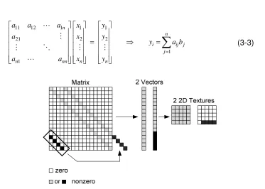
Figure 3.9 A banded sparse matrix ... 64
Figure 3.10 Store a banded sparse matrix on the GPU ... 64
Figure 3.11 Pack more nonzero into diagonal vector ... 65
Figure 3.12 Encode to the nonzero element in the random sparse matrix ... 66
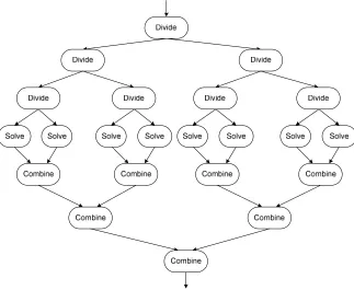
Figure 3.13 The process tree of Divide and Conquer pattern ... 72
Figure 3.14 Demonstration of the Merge-Sort algorithm ... 74
Figure 3.15 Coordination between Pipes-and-Filters in the push method ... 76
Figure 3.16 Coordination between Pipes-and-Filters in the pull method ... 76
Figure 3.17 Coordination between Pipes-and-Filters where both two filers are active .... 77
Figure 3.18 Communicating sequential elements pattern ... 78
Figure 3.19 The Processor Farms pattern ... 79
Figure 3.20 Cell CPU Architecture ... 80
Figure 4.1 The relationships of GPGPU’s parallel architectural pattern, programming framework and models. ... 84
vii
Figure 4.3 The conventional GPGPU architectural pattern ... 92
Figure 4.4 The new GPGPU architectural pattern with embedded unified pipeline ... 94
Figure 5.1 The convolution operation ... 103
Figure 5.2 Sequential program for the convolution operation ... 103
Figure 5.3 GPGPU programming model for filtering algorithms ... 105
Figure 5.4 The codes for data mapping ... 106
Figure 5.5 Fragment program to implement convolution operation ... 107
Figure 5.6 Data scatter through render-to-texture ... 108
Figure 5.7 Data splitting and storage in Framebuffer object ... 109
Figure 5.8 Convolution operation on the first part of metrological data shown in Fig5.7 110 Figure 5.9 Convolution operation on the ( n( n−1)+1)th part of metrological data ... 110
Figure 5.10 A primitive surface profile ... 111
Figure 5.11 Result of Gaussian filtering issued by MATLAB simulations ... 112
Figure 5.12 Result of GPGPU-based Gaussian filtering ... 112
Figure 6.1 Multi-level DWT and IDWT ... 119
Figure 6.2 The square decomposition scheme ... 124
Figure 6.3 The operational model of the GPGPU and wavelet-based denoising ... 125
Figure 6.4 The symmetrical periodic extension scheme ... 126
Figure 6.5 FP for edge extension ... 126
Figure 6.6 OpenGL instructions for controlling filtering and downsampling ... 127
Figure 6.7 Corresponding fragment program for filtering in horizontal dimension ... 128
viii
Figure 6.9 Fragment program for upsampling along vertical direction ... 130
Figure 6.10 The effect of upsampling ... 130
Figure 6.11 Noisy night-sky cityscape ... 131
Figure 6.12 Coefficients at decomposition level 1 ... 132
Figure 6.13 Coefficients at decomposition level 2 ... 132
Figure 6.14 Coefficients at decomposition level 3 ... 133
Figure 6.15 Noisy image (1024×960) ... 133
Figure 6.16 Denoising effects using the Db4 wavelet ... 134
Figure 6.17 Denoising effects on the image of night-sky cityscape ... 135
Figure 6.18 The noisy image of a sunflower ... 135
Figure 6.19 Denoising effects on the image of sunflower ... 136
Figure 7.1 Profiles of structured surface characterized by step and grooves ... 143
Figure 7.2 The optical path in a interferometer ... 144
Figure 7.3 Illustration of 2pi phase ambiguity ... 145
Figure 7.4 Intensity curve of interference signal at a scanned point ... 147
Figure 7.5 Intensity curve with different length of wavelength segment ... 148
Figure 7.6 Pack of grayscale image at various wavelength ... 150
Figure 7.7 Phase distribution in the wavelength segment ... 151
Figure 7.8 The curve of 2π phase shift ... 151
Figure 7.9 The curve of phase shift within chosen wavelength segment ... 152
Figure 7.10 Grid of thread blocks ... 155
ix
Figure 7.12 Heterogeneous programming in CUDA applications ... 158
Figure 7.13 The intensity of interference signal at a specific wavelength ... 163
Figure 7.14 FFT on different pixels ... 164
Figure 7.15 Flow of CUDA-based data processing in OSSI ... 169
Figure 7.16 The surface profile (wavelength number=64) ... 174
Figure 7.17 The surface profile (wavelength number=128) ... 175
Figure 7.18 The surface profile (wavelength number=300) ... 175
Figure 7.19 The surface profile (wavelength number=400) ... 175
Figure 8.1 Diagram of linear time-invariant system ... 179
x
List of Tables
Table 2.1 Key specifications of Shader Models (SM) ... 35
Table 3.1 Architectural patterns classification... 71
Table 5.1 Processing time of GPGPU program and MATLAB simulation ... 112
Table 5.2 Processing time of solutions with data dividing and without dividing ... 113
Table 6.1 Runtime comparisons on different image size (in ms) ... 137
Table 6.2 Breakdown of computational time (in ms) ... 138
Table 6.3 Runtime of key steps in thresholding (in ms) ... 138
Table 6.4 Proportional benchmarking of GPU-CPU data transfer latency ... 139
Table 6.5 Runtime of sub-stages on various image sizes using Wong’s method (in ms) ... 139
Table 6.6 Runtime comparisons on different image size (in ms) ... 141
Table 7.1 Data types in CUFFT ... 159
Table 7.2 API functions in CUFFT ... 160
Table 7.3 Multi-thread and Multi-stream Performance Comparison ... 174
xi
List of Abbreviation
AI Artificial Intelligence ALU Arithmetic Logic Unit
API Application Programming Interface ARB Architecture Review Board
ASIC Application-Specific Integrated Circuit ASMP Asymmetric Multiprocessing
CFD Computational Fluid Dynamics Cg C for Graphics
CMT Chip Multithreading Technology COM Component Object Model CPT Centre of Precision Technology CWT Continuous Wavelet Transform CUDA Compute Unified Device Architecture D3D Direct3D
DMA Direct Memory Access DFT Discrete Fourier Transform DWT Discrete Wavelet Transform EIB Element Interconnect Bus FBO Frame Buffer Object FBS Filter Bank Scheme FFP Fixed Function Pipe-line FFT Fast Fourier Transform FP Floating-Point
xii GDI Graphics Device Interface GE Geometry Engine
GKS Graphical Kernel System GL Graphics Library
GLSL OpenGL Shading Language GPU Graphics Processing Unit
GPGPU General-Purpose Computing on GPU GRF Gaussian Regression Filter
GUI Graphics User Interface HLSL High-Level Shading Language HP Hewlett-Packard
HPC High Performance Computing IC Integrated Circuit
IDWT Inverse Discrete Wavelet Transform IPPS Integrated Parallel Processing Systems LTI Linear Time-invariant
MAD Multiply and Add
MIMD Multiple Instruction Multiple Data MISD Multiple Instruction Single Data MPI Message Passing Interface MSE Mean Square Error
OpenCL Open Computing Language OpenGL Open Graphics Library OPD Optical Path Difference
OSSI Optical Spectral Scanning Interferometry Pbuffer Pixel buffer
xiii PFP Programmable Function Pipeline
PHIGS Programmer's Hierarchical Interactive Graphics System PPE Power Processing Element
PSNR Peak Signal-to-Noise Ratio PVM Parallel Virtual Machine RC Resistor and Capacitor R & D Research and Development RGBA Red, Green, Blue and Alpha RISC Reduced Instruction Set Computer SDK Software Development Kit
SGI Silicon Graphics Inc.
SIMD Single Instruction Multiple Data SISD Single Instruction Single Data SM3 Shader Model 3.0
SM4 Shader Model 4.0
SMP Symmetric Multiprocessor
SMT Simultaneous Multithreading Technology SNR Signal to Noise Ratio
SPE Synergistic Processing Elements SSE Streaming SIMD Extensions T & L Transform and Lighting VBO Vertex Buffer Object
xiv
Table of Contents
Acknowledgments ... I
Abstract……….. ... ii
List of Publications ... iv
List of Figures………. ... v
List of Tables………… ... x
List of Abbreviation ... xi
Chapter 1 Introduction ... 1
1.1 Research Motivation ... 2
1.2 Research Questions and Evaluation Strategy ... 4
1.3 Outlines ... 6
Chapter 2 Review of Related Work ... 8
2.1 Levels of Parallelism ... 8
2.2 Types of Parallel Hardware ... 12
2.2.1 Multicore Structure ... 13
2.2.2 Symmetric/Asymmetric Multiprocessor Structure ... 13
2.2.3 Cluster Structure ... 14
2.2.4 Grid Structure ... 15
2.3 Overview of GPU Architecture ... 15
xv
2.3.2 Evolution of GPU’s Hardware Architecture ... 17
2.4 Graphics APIs and Shading Languages ... 29
2.4.1 The Direct3D Route ... 30
2.4.2 The OpenGL Route ... 32
2.4.3 Dedicated GPU Languages -- Cg and HLSL ... 33
2.4.4 Evolution of Shader Models ... 34
2.5 Languages for General-Purpose Computations ... 35
2.5.1 Brook for GPUs ... 36
2.5.2 CUDA – “Compute Unified Device Architecture” ... 36
2.5.3 CTM – “Close-to-the-Metal” ... 37
2.6 Summary ... 38
Chapter 3 General-Purpose Computing on Graphics Card and Architectural Pattern in Parallel Computing ... 40
3.1 Foundational Function Blocks: Streams and Kernels ... 41
3.1.1 Data Streams ... 42
3.1.2 Instruction kernels ... 43
3.2 GPGPU Task Computing ... 44
3.3 Render-to-Texture ... 48
3.4 Embedded Parallelism in GPGPU ... 51
3.4.1 The Stream Programming Model ... 52
3.4.2 Flow Control... 55
xvi
3.5 Optimization of GPGPU in Linear Arithmetic Operations ... 63
3.5.1 Representation of Banded Sparse Matrices ... 63
3.5.2 Optimized Implementation on Random Sparse Matrix ... 65
3.5.3 Further Discussion ... 67
3.6 Process Decomposition in Parallel Computing ... 68
3.7 Classification of Parallel Architectural Patterns ... 70
3.7.1 Divide-and-Conquer ... 72
3.7.2 Pipes-and-Filters ... 75
3.7.3 Communicating Sequential Elements ... 77
3.7.4 Processor Farms ... 79
3.8 Summary ... 81
Chapter 4 General Programming Framework of GPGPU Applications ... 83
4.1 GPGPU’s Parallel Architectural Pattern ... 83
4.2 Implementations in Programming Framework for Parallel Systems ... 85
4.3 GPGPU’s Programming Framework ... 90
4.3.1 Programming Framework for Conventional Graphics Pipeline ... 91
4.3.2 Programming Framework for Unified Pipeline ... 93
4.3.3 Programming Model Design ... 95
4.4 Summary ... 96
Chapter 5 Accelerated Filtering Algorithms for Surface Profiling ... 98
xvii
5.2 Filtering Algorithm Analysis ... 102
5.3 Hardware Acceleration for Filtering Algorithms ... 104
5.3.1 The GPGPU Programming Model ... 105
5.3.2 Implementation Details ... 105
5.4 Test and Performance Evaluation ... 111
5.4.1 Test Results ... 111
5.4.2 Performance Evaluation ... 113
5.4.3 Accuracy Analysis ... 114
5.5 Summary ... 115
Chapter 6 Parallel Implementation on Wavelet-based Image Denoising .. 116
6.1 Wavelet-based Denoising ... 116
6.1.1 Analysis of the Wavelet Transform ... 117
6.1.2 Thresholding Strategy ... 119
6.2 Wavelet-based Denoising on GPU ... 122
6.3 Technical Specifications of the GPU Implementation ... 125
6.3.1 Decomposition ... 125
6.3.2 Thresholding ... 128
6.3.3 Reconstruction ... 129
6.4 Test and Performance Evaluation ... 131
6.4.1 Results of Decomposition ... 131
xviii
6.4.3 Evaluation on Computational Efficiency ... 136
6.5 Summary ... 141
Chapter 7 Unified Pipeline Model-based Parallel Processing for Spectral Scanning Interferometry ... 142
7.1 Surface Metrology Using Optical Spectral Scanning Interferometry ... 142
7.1.1 The Principle of Surface Metrology Using Monochromatic Interferometry ... 143
7.1.2 The Principle of Optical Spectral Scanning Interferometry ... 145
7.2 Data Processing in Optical Spectral Scanning Interferometry ... 148
7.3 Compute Unified Device Architecture (CUDA) ... 152
7.3.1 Thread Hierarchy ... 153
7.3.2 Memory Hierarchy... 156
7.3.3 Host and Device ... 158
7.3.4 The programming API -- CUFFT ... 159
7.4 CUDA-based Data Processing in OSSI ... 162
7.4.1 Initialization ... 162
7.4.2 FFT and Inverse FFT ... 163
7.4.3 Computing the Absolute Phase Shift ... 165
7.4.4 Visualization of Processed Results ... 169
7.5 Performance Evaluation ... 173
7.6 Summary ... 176
xix
8.1 GPGPU-based LTI Systems Analysis ... 178
8.1.1 Time Domain Analysis on GPGPU-based LTI Systems ... 178
8.1.2 Frequency Domain Analysis on GPGPU-based LTI Systems ... 182
8.2 Final Discussions ... 183
Chapter 9 Contributions and Future Works ... 186
9.1 Contributions ... 186
9.2 Future Works ... 188
References………. ... 191
1
Chapter 1
Introduction
High Performance Computing (HPC) has been a widely studied topic in scientific research and engineering applications since the appearance of modern computers in the 1940s. A straightforward approach to this goal is to continually increase the processors’ processing speed through technological innovations such as scaling CPU’s frequency. However, a processor’s frequency is limited to its power consumption for the reason that the core’s power usage is scaled to its frequency (Rabaey, 1996). The limitation of power consumption actually hampered the trend of continuously increasing of CPU’s processing power for HPC.
Another obvious approach to the goal is through better “structuring” of the process and data to maximize the efficiency of the computer. The fact that massive amounts of data can often be processed by the same function simultaneously; and/or many tasks can be performed concurrently for scientific computations had encouraged the extensive researches on the so-called “parallelism” in contemporary computer architectures. Generally speaking, the parallelism in computer architectures evolves along two directions -- a single computer with multiple cores or multiple processors such as supercomputer; or multiple computers working together on similar tasks through structures such as computer clusters or computer grids (Ian Foster, 1995; Sinnen, 2007). Both solutions have raised the issue of the cost of building those parallel computers, which often results in a dilemma between the computational performance and the hardware cost. In the past, parallel computers were often restricted to high profile government funded major scientific projects across the globe.
2
This situation had resulted in the innovation and production of the so-called consumer-level parallel processors; the best representative of which are today’s Graphics Processing Units (GPUs). With a peak-speed performance over 933 Gigaflops (GFLOPS), the computation capacity of the latest GPUs dwarf today’s commodity CPUs in terms of speed and cost. With the increasing programmability-empowered flexibility of modern GPUs, many researches and development projects have been focusing on the conception of general-purpose computing on GPU (GPGPU) with the aim of tacking computationally intensive tasks previously only processed on CPUs. Many traditional parallel computing paradigms and techniques have been mapped to GPGPU, including grid and cluster, synchronous and asynchronous processes.
This research project explored the concept of stream computing within the GPU design and programming paradigms. It then devised a programming framework for GPGPU applications, specifically for handling data intensive metrological analyses, on the basis of the inherent parallel architecture patterns of GPUs. The devised programming framework is then used for design the algorithm mapping models for GPGPU-based signal and image processing tasks.
1.1 Research Motivation
3
systems, and to benchmark its hardware acceleration factors as well as the corresponding realization criteria.
In detail, the motivations of using the GPU for surface metrological data processing can be detailed as follows:
• A GPU is one of the most cost-effective, easily accessible forms of hardware available for implementing parallel processing among many existing parallel architectures (Owens et al., 2007). A typical GPU, equipped with several hundreds of arithmetic processing cores, will cost only a fraction of the price for a multiprocessor array with equivalent numerical processing power.
• Most researches reviewed in this project only focused on the segregated performance of algorithms run on GPUs. In practice, the GPU is still only a coprocessor of the CPU despite its amazing computing speed, i.e., a complete GPGPU program must also include settings and tasks run on CPU. Therefore, the performance evaluation of GPGPU implementations should also take into account the tasks performed on the CPU and the corresponding overhead of data communication in between the two. The ambiguity on this point has raised doubts on the GPGPU’s practical values in engineering domains. This research tackles the challenges through exploring the performance of GPGPU-based surface metrological analysis/tasks in a comprehensive range of practical settings.
4
of GPUs as mainstream computing devices. The experiments designed in this work aligned themselves to the target of obtaining a clear conception and practical approach to GPGPU programming. In addition, this effort is accompanied by the main GPU vendors such as ATi and Nvidia corporation, who have managed a continuous evolvement of GPU hardware architectures, for example, a uniform platform for the GPU programming. The research also investigated the influence of the GPU’s hardware evolution on the future GPGPU programming framework.
• A rich and advanced body of work is also documented in this report on the architecture patterns developed for GPUs in the last decade. These centred around the parallel architectures, stemmed from CPU paradigms. The work aimed to investigate the architectural patterns of various GPUs, to form a generic guideline for the future design of application frameworks for GPGPU programming.
Driven by above goals and targets, the research works in this project were designed and developed around a practical engineering domain, the surface metrology. This was carried out in collaboration with the Centre of Precision Technology (CPT) at the University of Huddersfield, which is a centre research on surface metrology. The outcome of the research is expected to have potential value for the wider engineering and scientific communities.
1.2 Research Questions and Evaluation Strategy
5
diversions. Therefore, it is of vital importance to define common principles or rules to guide the GPGPU application design, so those principles can be extensively applied to cover the different generations of hardware and software tools. Therefore, this is the first question that needs to be tackled within this thesis.
As stated in the aforementioned research motivations, the thesis is based on the practical engineering applications for data analysis and processing in surface metrology. The ultimate task of surface metrology is to profile a surface using the measured and processed data, to which the ideal solutions are to increase the number of samples and to employ more sophisticated algorithms to achieve higher data accuracy, but often with the deteriorating computational efficiency as a cost. Therefore, the challenge of data analysis in surface metrology is largely attributed to the dilemma of data accuracy and computational efficiency. The second challenge faced by this research is whether the GPGPU concept and existing techniques can sufficiently support a flexible solution to the complex processes normally involved in metrological data operations. The feasibility and practicality of the solution will be evaluated by two vital parameters - the speed up factors and data accuracy of the deployed GPGPU programs. It is noted that the result of the evaluation will determine the validity of the designed GPGPU programming models
6
validated through testing the run time of data visualization and its weightings in the overall application time.
1.3 Outlines
7
8
Chapter 2
Review of Related Work
Parallel processing is a form of computation in which data are either being processed by the same group of functions simultaneously; or multiple tasks are carried out on the same input concurrently. There are four levels of parallelism in contemporary computers at bit, instruction, data, and task levels (Sinnen, 2007).
In this chapter, the 4 levels of parallelization are reviewed and an overview on the evolution of GPU hardware structures and their parallel programming tools are also provided. As a coprocessor, a modern GPU achieves data-level parallelism through its own dedicated memory (DRAM) and columns of arithmetic cores, each consists of a group of registers, shared memory, caches, etc. The innovative design and its continuous evolution led to the raw processing ability of GPUs exceeded that of CPUs by the start of the New Millennium. The latest Nvidia Tesla C1060 GPU released in 2008 could sustain up to 933 Gigaflops (GFLOPS1) while the Intel Pentium4 CPU appeared on market approximately same time can only manage 104 Gigaflops when assisting SSE (Streaming SIMD Extensions) instruction set were employed (Nvidia Corporation, 2009). At the same time, the improvement on GPUs has ensured its flexibility, which is backed up by the programmability, continuous renovation and update of GPU’s hardware structure. It has achieved an amazing annual updating rate of 2.8 since 1993 (Owens et al., 2007).
2.1 Levels of Parallelism
Parallelism in computing is generally classified into bit-level, instruction-level, data-level, and task-level which are closely related to processors’ architectures (Almasi and Gottlieb,1990).
1
9
The bit-level parallelism was the first form of parallel computing and was introduced by the first appearance of the very-large-scale integration (VLSI) based fabrication technology of integrated circuit (Sina et al, 2003). The concept was driven by the demand for doubling computer word sizes that represents the amount of information the processor can execute per cycle (EI-Rewini and Abd-El-Barr, 2005). Chronologically, 4-bit processors were substituted by 8-bit ones, and then 16-bit to 32-bit and 64-bit ones nowadays. Although the concept of bit-level parallelism is quite simple, it is essential for many advanced extensions and applications.
Instruction-level parallelism reorders instructions in a computer program and then combines them into groups that can be executed in parallel without altering the ultimate result. In modern processors, an instruction is implemented through a multi-stage instruction pipeline, in which each phase corresponds to a different processor’s action (Berkovich, 1998). Different stages of variant instructions can therefore be overlapped to achieve instruction-level parallelism. For example, a Reduced Instruction Set Computer (RISC) processor has a five-stage pipeline which consists of fetch, decode, execute, memory access, and write back operations (Steve, 1995). The instruction-level parallelism is achieved through the following canonical orders, where the grey column stands for:
Figure 2.1 Different stage overlap of instruction pipeline in RISC machine
In addition, some processors which are known as superscalar processors can implement multiple instructions simultaneously if these instructions have no data dependency between them (Goossens, 2001).
10
loop-level parallelism. Based on the relationships between instructions and data streams, Flynn summarized in 1972, four categories of common computing architectures, known as Flynn’s taxonomy (Foster, 1995):
• Single Instruction Stream, Single Data Stream (SISD)
• Multiple Instruction Stream, Single Data Stream (MISD)
• Single Instruction Stream, Multiple Data Stream (SIMD)
• Multiple Instruction Stream, Multiple Data Stream (MIMD)
Among those, data parallelism is classified as a form of SIMD, which is normally achieved in a multiprocessor system, for example, consider a dual-core CPU unit carrying out a matrix addition operation. At runtime, the first core of that CPU adds all elements from the top half of the two matrices, while the second core adds all elements from the bottom half of the matrices. With the two cores working in parallel, the matrix addition will take half the time it would have if operations were performed in serial on a single-core CPU.
Compared with data parallelism in which the same instruction is implemented on multiple data sets, the task parallelism invokes a parallel program which issues independent calculations on either a single or multiple data streams (Rastello et al., 2003). Based on this definition, the aforementioned MISD and MIMD are both belong to the genre of task parallelism. However, some workers (Schneider and Rossignac, 1995; David et al., 1994) argue that MISD is actually a type of instruction-level parallelism, since the data streams processed by the instructions are the same as indicated in Figure 2.1. In a multi-processor system, task parallelism is realized when each processor executes a different thread (or process) on the data. The threads may execute the same or different instructions. In the general case, different threads communicate with each other through passing data from one thread to the next as part of a workflow (William and Rajeev, 2007).
11
streams are the output or input of memory. The hardware structures of the MISD, SIMD and MIMD are shown in Figure 2.2 to Figure 2.4 respectively.
Figure 2.2 Models of a MISD architecture
12
Figure 2.4 Models of a MIMD architecture
2.2 Types of Parallel Hardware
Memory units are a key element in all computing devices, where initial, intermediate, and resulting data are stored temporarily for further processes. Global memory in a parallel computing architecture can be a shared memory which is accessed by all processing elements in the same memory address; or a distributed memory in which each processing element has its own local address space (Foster, 1995). The term “distributed” means the memory is either logically distributed, or physically distributed. A shared and distributed memory is an integration of the two forms, in which every processing element has its own local memory as well as the ability to access memories on other non-local processors (Huang et al., 2004). Access to local memory is normally faster than to non-local memories.
13
2.2.1 Multicore Structure
There are multiple execution units called cores in a multicore processor. The style of the instruction implementation in a multicore processor is different from that in a superscalar processor. A superscalar processor can implement several instructions per clock-cycle from one instruction stream - the so-called thread. In contrast, a multicore processor can implement several instructions per clock-cycle from several instruction streams (Thomaszewski et al., 2008). Recent hardware advancement has proven that actually each core in a multicore processor can act as a superscalar one as well, i.e., each core implements several instructions from one instruction stream on every cycle (Steven et al., 1997).
In terms of actual production, the Intel's Hyper-Threading (Intel Corporation, 2007) is one of the best known simultaneous multithreading machine which is an early form of pseudo-multicoreism, while Intel's Core and Core 2 processor series are the true-meaning multicore architectures (Intel Corporation, 2008). The latest IBM's Cell CPU is another representative form of the multicore technology (Gschwind, 2007).
2.2.2 Symmetric/Asymmetric Multiprocessor Structure
Multicore processor systems employ a single processor that has multiple pipelines for integer and floating-point operations. Multiple identical processors can also be connected to a single shared main memory to form a symmetric multiprocessor (SMP), in which the processors are capable of accessing the same shared memory through a bus or crossbar switch (Kaya, 2005). The SMP system allows any processors to carry out any task simultaneously. Based on properly designed operating system, a SMP system is able to readily transfer tasks across processors to distribute the workload evenly.
14
limits the scale of the processor numbers in a SMP system, which results in the fact that the processors in a SMP system is normally less than 32. The alternative solution for the SMP is an asymmetric multiprocessing (ASMP) structure in which a group of separate specialized processors are employed for specific tasks (Robert et al., 1998). In contrast to the SMP of assigning all of the tasks in the system identically, an ASMP system only assigns specific tasks on specific processors. The common ASMP structure is a kind of clustered multiprocessors in which just a portion of the entire memory can be accessed by all processors (Cai et al., 2004).
2.2.3 Cluster Structure
As indicated above, ASMP structures can practically be categorized as the cluster structure according to Flynn’s taxonomy that can be viewed as a way of building low-cost and distributed-memory MIMD computers. Gene Amdahl from IBM, who put forward Amdahl's Law for parallel computing, defined the distinction between the multiprocessor computing and the cluster computing in 1967(Moncrieff et al., 1996). Stated simply, the main difference is the communication modes where in multiprocessor computing it is issued inside the computer through internal bus structures, while in cluster computing it is based on the outside network such as local network, wide access network(WAN), or the Internet.
Based on the packet switching networks invented in 1962 (Natalia and Victor, 2006), the first commodity network employing computer cluster theory was presented by the ARPANET project in 1969 (Douglas, 2009). As the ARPANET evolved into the Internet, the original computer cluster connected by a Packet switching network also grew into the “proper” cluster in which the communications between the nodes uses the TCP/IP protocol, based on the Ethernet network framework (Thomas and Zsolt, 2007).
15
computing in general terms, the VAXcluster also support the shared file systems and the peripheral devices. Following the success of VAXcluster, various commercial clusters were released in turn, such as the Tandem Himalaya and the IBM S/390 Parallel Sysplex, both released in 1994 (Thomas and Zsolt, 2007). With the growing maturity of cluster computers, the parallel computing ethos has encouraged further development into techniques such as grid computing where more focus has been put into the throughput of a computing utility rather than running a deliberately designed, optimized, and tightly-coupled jobs.
2.2.4 Grid Structure
In grid computing, a number of computers (irrespective of their individual architectures) are loosely connected via a network. In the most extreme case, each machine (including the properties of connections between them) is assumed to be different. This makes for an extremely heterogeneous system, which requires the coarsest level of parallelization since the work must be divided into independent units that can be completed on different computers at different speed, and returned to the main solution coordinator at any time and in any order without compromising the integrity of the solution (Thomas and Zsolt, 2007). Although there are tasks that are naturally amenable to this level of parallelization, a broader applicability of this approach requires much further research and infrastructure development. Successfully tested cases so far has been focused on the analysis of very large sets of independent data blocks, in which the problem lies in the total size of data to be analyzed.
2.3 Overview of GPU Architecture
2.3.1 The Origins of Graphics Processing
16
software capacity and adaptability. The Graphical Kernel System (GKS) (Hopgood et al., 1983; Enderle et al., 1984) and Programmer's Hierarchical Interactive Graphics System (PHIGS) (Howard et al., 1991) were representative standards. A typical graphics pipeline is defined by those standards as depicted in Figure 2.5.
Figure 2.5 Abstract graphics pipeline defined in PHIGS
In the early 1980s, “new” graphics processors, that had been inspired by the innovative geometry engine (GE), were launched by various manufacturers. Graphics cards developed at this stage were dominated by graphics processor, which was an integrated chip on the computer motherboard with built in geometrical functions. The core of a GE is the support for floating point number computation between any 4-component vectors (Clark, 1982). These computations were used for coordinate transformation, blending and projection. A complete three-dimensional (3D) graphics pipeline can be accomplished by 12 such geometrical elements. James Clark, the designer of the geometry engine, then setup Silicon Graphics Inc. (SGI) in 1981 on the basis of GE technology (Watt, 1999). SGI had a significant influence on the development of computer graphics in the following decade; Graphics Library (GL) and the subsequent OpenGL became the industry standard of GUI for graphics processing.
17
they were only viewed as graphics accelerators, instead of as a programmable core and a flexible processor. In the era of CPU dominance, a prominent event was the adoption of Single Instruction Multiple Data (SIMD) for fragment operations in 1992. SIMD is a technique traditionally employed by parallel computing applications to achieve data-level parallelism. In 1980, a research group at the University of North Carolina in USA first employed SIMD in their graphics software, Pixel-Planes (Fuchs and Poulton, 1981; Fuchs et al., 1989) and Pixel-Flow (Molnar et al., 1992), which marked the take-off of dedicated vector-computation -- though still at the software level and driven by CPU.
2.3.2 Evolution of GPU’s Hardware Architecture
The evolution of post-90s GPUs can be divided into 5 stages, display adapter, transform and lighting (T & L) chip, programmable shader, CineFX engine, GPGPU unit, and multi-core.
• Stage 1 – mid 1990s
18
released their graphics cards that had similar functions of 3DFX VooDoo, the Nvidia Riva TNT and ATI Rang series.
Although a great leap from the earlier graphics software based graphics processors, the key problem of the products at the time was that the actual geometry processing was still carried out on CPU, which presented a heavy burden on CPU efficiency and seriously implicated the real-time performance of many 3D applications such as computer games. The abstract of the mid-90s graphics pipeline is depicted in Figure 2.6.
Figure 2.6 Abstract graphics pipeline between in 1995 and 1998
• Stage 2 – late 1990s
19
Figure 2.7 Abstract graphics pipeline (integrated T & L) at late 1990s
The shifting of the T&L from CPU to GPU was a great boost to the real-time polygon/vertex processing capacity, while the idealised local illumination models – directional, point, and spot – had simplified the computation and greatly increased the final rendering quality. Figure 2.8(a) and (b) highlight the enhanced GPU capability on polygon numbers and lighting.
20
[image:41.595.209.417.113.267.2](b) Lighting effect of GeForce 256
Figure 2.8 The enhanced GPU capability (Courtesy to Nvidia Corporation)
In contrast to a previous generation GPU -- Riva TNT2 which had just 2 parallel rendering pipeline, GeForce 256 has provided 4 parallel rendering pipelines. Each pipeline has a dedicated texture unit to access textures in parallel in each rendering pass (Nvidia Corporation, 2009). However, most of the GPU functions of this generation were still largely hard-wired in the physical IC chips and provided little flexibility for customization.
• Stage 3 – early 2003
21
with a less detailed smooth surface rendered by a fixed-function graphics pipeline.
[image:42.595.115.508.160.331.2]
(a) (b)
Figure 2.9 A 3D head rendered by vertex shader and fixed-function graphics pipeline respectively (Courtesy to Nvidia Corporation)
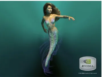
In 2002, Nvidia released its GeForce 4 series in which the programmable vertex and pixel shaders were both available. The GeForce 4 series added the static and dynamic flow control in its design, which was absent in the GeFoece 3. While the vertex shader controls the vertex attributes, the pixel shader manipulates each pixel’s colour fill-up that is issued by certain transfer functions. In a demo rendered clip released by Nvidia, as shown in Figure 2.10, the intricate details of the mermaid’s hair and the minute tail shift are controlled by specific pixel shaders and polynomial transfer functions designed by graphics programmers.
[image:42.595.223.402.561.697.2]22
As well as exploiting the newly introduced programmable vertex and pixel shaders of the graphics cards at the time, the processing speed was further accelerated by the continuously expanding of the number of parallel rendering streams. For example, up to 16 textures can be processed simultaneously in the GeForce 4 series, which had become the technical foundation for high-definition graphics. ATi corporation, another heavy-weight GPU vendor, has also had its flagship product – the Radeon 8000 series – pushed to the market around the same period with the programmability as the key selling point (ATI Corporation, 2007). Generally, the hardware architecture of GPUs at this stage can be summarized as in Figure 2.11.
Figure 2.11 Hardware abstracts of GPUs with programmable vertex and pixel shaders
• Stage 4 – mid 2000s
23
will always be a problem for GPU designers, the CineFX engine has introduced the intellisample technology to alleviate this dilemma. The intellisample technology is formed by two key parts – Colour Compression and Dynamic Gamma Correction, which are integrated in GPU’s IC chips. Colour Compression ensures image quality through the so-called lossless compression, while the Dynamic Gamma Correction boosts the image vividness through using the adaptive texture filtering technology.
24
Figure 2.12 Model of the graphics pipeline of GPU released in 2004-2005
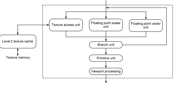
Since this project will largely based on the new found power of vertex/pixel manipulation of this generation of GPUs and beyond, it is useful to explain the actual workflow of it. The logic flow of vertex shader embedded in the GeForce 6800/7800 series is depicted in Figure 2.13 (Collange et al, 2007). Its working order can be simplified into the following phases: the host memory on CPU side sends the vertices’ information across the CPU/GPU border, a vertex shader is then initiated to perform transformational (translation, rotation, and scaling) operations and local illumination calculation. Most of the computation will be based on arithmetic terms such as Multiply and Add (MAD), Exponential functions (exp, log), Trigonometric functions (sin, cos) and Reciprocal functions (1/x and1/ x) to form physics equations, while the innovative texture memory access has enabled vivid rendering effect and real-time simulations such as shape deformity.
25
The workflow of the pixel shader can be depicted as in Figure 2.14 (Collange et al, 2007). There are two floating-point (FP) unit appended with a Mini Arithmetic Logic Unit (ALU) that promotes the computation efficiency of FP numbers. The first FP unit can carry out up to 4 MAD operation at a time and accessing textures via the texture unit. The result is then sent to the second FP unit for up to 4 further MADs. A pixel shader of this model also includes a level-1 texture cache for rapid data accessing.
Figure 2.14 Pixel shader model of Nvidia GeForce 6800/7800 released in 2004-05 (Courtesy to Collange)
• Stage 5 – current trend
With the evolution of shader technologies, the concept of General-Purpose computing on the GPU (GPGPU) has become more and more popular, with the aim of addressing problems based on data-level parallelism. The earliest GPGPU programs in 2001 (Owens et al., 2007) was mainly focused on the areas of tailor-made applications such as image processing and matrix operations, while the latest GPGPU development has seen its extension into the applications of pattern recognition, signal processing, and physics simulation (Owens et al., 2007).
26
is a tedious work for developers who are unfamiliar to graphics programming. Secondly, sometimes serious waste can occurred when work is distributing between vertex and pixel shader. The first problem requires intensive mathematical skills, while the second one demands knowledge of computer hardware, which are often unfamiliar to application developers.
The GPU’s parallel computational capability is largely determined by the number of rendering pipelines available. The number of vertex and pixel shaders available in traditional graphics pipelines is determined by the anticipated ratio of the need for the functions during rendering. For example, the Radeon X1800 has 8 vertex shaders and 16 pixel shaders (ATI Corporation, 2007), and the GeForce 7800 has 8 vertex shaders and 24 pixel shaders (Nvidia Corporation, 2009); the ratio is 1:2 and 1:3 respectively. The workflow in a GPU for transforming 3D geometries into 2D graphics follows the order of vertex shader, pixel shader, and then to the framebuffer. Thus the actual number of parallel streams is limited by the narrower section of the pipeline, in this case, the number of vertex shaders. However, most of the GPU vendors advertise the number of rendering pipelines by emphasizing on the number of pixel shaders only, for marketing reasons. Some might argue that most of the successful GPGPU showcases are implemented on pixel shaders alone. Though the matter of fact is, without careful and pains-takingly tedious balancing of the workload, a problem can arise in which either all the vertex shaders are heavily working while most of the pixel shaders are idle, or vice versa. This situation can be illustrated by the following figure.
27
To solve the problem of workload imbalance between dedicated pixel shaders and vertex shaders, Nvidia and ATI released Geforce 8800 (Nvidia Corporation, 2009) and Radeon HD2000 (ATI Corporation, 2007) successively in 2006. These two GPUs have employed a brand-new framework which adopted a unified pipeline architecture without a distinctive vertex and pixel shader borderline, as depicted in Figure 2.16.
Unified shader
Pixel
workload Heavy geometry workload
Heavy pixel workload Vertex workload
Unified shader
Vertex workload Pixel workload
Figure 2.16 Workload allocation in unified pipeline
28
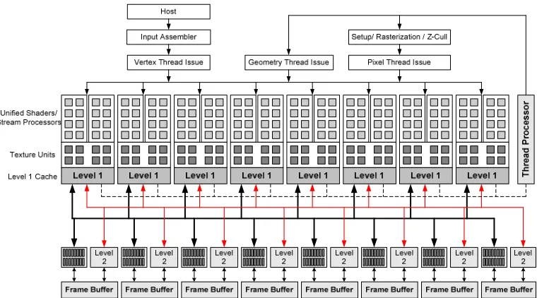
Figure 2.17 Architecture of unified shader arrangement (Courtesy to Nvidia Corporation)
In this design, the 128 unified shaders are clustered into 8 groups. Each group therefore consists of 16 unified shaders for accessing 8 texture units and a number of level 1 and level 2 caches. It is also apparent in this design that each unified shader can export the processed data to be “recycled” by other streams and practically forming the loop of thread processors. This GPU architecture guaranteed it can operate as a SIMD parallel processor with high efficiency. All the GPUs of this generation support IEEE754 double precision floating-point number arithmetic standard.
29
Supercomputers have equipped with 960 cores for larger scale applications (Nvidia Corporation, 2009).
2.4 Graphics APIs and Shading Languages
30
Figure 2.18 PC graphics API architecture
2.4.1 The Direct3D Route
The functionality of Microsoft’s DirectX Application Programming Interface (API) is wrapped in the form of Component Object Model (COM) and managed code interfaces. DirectX constitutes graphics, audio, input, and network cores, depending on the version (Adams, 2003). Among the components, DirectDraw (prior to version 8) is for defining 2D graphics directly on the screen space and the Direct3D (D3D) is for handling 3D graphical task (Adams, 2003). Prior to DirectX, OpenGL was the dominant API on the market for consumer level rendering tasks. The situation finally changed with the formal publication of DirectX 7 by Microsoft in September 1999 after a prolonged trial period of its earlier versions.
A prominent feature of the Direct3D API in DirectX 7 is the new addition of the Transform and Lightning (T & L) pipeline hard-wired on the graphics card, which first conjoined the speed and quality of the computation of expensive lighting and geometrical calculations. The flagship off-the-shelf product at that time was Nvidia’s GeForce 256. Although the joint force of the DirectX 7 software and the GeForce 256 hardware brought PCs into the GPU era, the pattern of Fixed Function Pipe-line (FFP) only allowed limited number of graphical and geometrical algorithms to be accessed in the configuration style, rather than programmed to specification.
31
hardware-routed T & L in Direct3D 7 was formally substituted by vertex and pixel shader techniques in Direct3D 8, which made the GPU a true programmable processor. However, in Direct3D 8 shaders have to be programmed in assembly language, which is hard to master for most application-level programmers. The Direct3D 8 series introduced shader models 1.0/1.1/1.3/1.4 successively with the early Nvidia GPU products supported Shader models 1.0/1.1/1.3, and its ATI counterparts supported all versions of shader model 1 series (Szirmay-Kalos et al., 2008).
In December 2002 Microsoft released its most famous and successful Direct3D 9 API which supports improved shader model 2.0 and 3.0 (Szirmay-Kalos et al., 2008). Shader model 2.0 added static flow control to the vertex shader, and Shader model 3.0 enabled static and dynamic flow control of both the vertex and pixel shaders. Apart from the extension of the supported shader instructions, the most prominent feature of Direct3D 9 is its support for the 64-bit RGBA color in pixel shading, and the 128-bit precision (32-bit for each colour channel) floating-point computation (Luna, 2003), which further improved the visual effect and rendering quality.
32
2.4.2 The OpenGL Route
Another identical route to access the GPU feature set is through the OpenGL. OpenGL (Open Graphics Library) was originated from the IRIS GL that was developed by the high-end workstation manufacturer Silicon Graphics (SGI). The steering group of this API – the OpenGL Architecture Review Board (ARB), which was formed by peoples from companies such as SGI, Intel, IBM, NVIDIA, ATi, Microsoft, Apple, was founded after the SGI’s first release of OpenGL 1.0 in July 1992. One of the key tasks of the OpenGL ARB is producing an industry standard for OpenGL, and its tool kits, through common agreements among the ARB members. The approved standards are then published as specifications based on the C programming language. Only those APIs that passed all the tests regulated by the specification can be referred as official OpenGL. The first product of this process, OpenGL 1.1, was formally released in 1995 (Hill, 2001).
The original OpenGL specification serves two main purposes (Hill, 2001):
1) To insulate the complexities of interfacing with various 3D graphics accelerators, including GPUs, by exposing to programmers a single and uniform API;
2) To encapsulate the varying capabilities of hardware structures through enforcing all implementations to support the full OpenGL feature set.
33
of the popular shading languages to develop interactive graphics and visualisation applications across operation systems from UNIX, Macintosh, Microsoft Windows, to Linux. This interchange ability enabled programmers to easily transfer their programs across most major commercial operating systems and hardware platforms.
In 2004 3Dlabs, a UK semiconductor company, substituted the dominant role of the SGI in the OpenGL ARB and unleashed the OpenGL 2.0 on the basis of OpenGL 1.5. It greatly improved the efficiency for some common operations from the previous versions and also added new features on creating photo-realistic, real-time 3D graphics that can be referred on SGI’s website (Silicon Graphics Inc., 2005). The latest development has seen OpenGL 3.0 becoming widely available with roughly equivalent features and powers to D3D10.
2.4.3 Dedicated GPU Languages -- Cg and HLSL
The earliest form of shading languages is constituted by assembly instructions such as ‘mov’ and ‘mod’. Although high on operating efficiency, in practice they are difficult to use and maintain. With the growth of the complexity of shader programs, the limitations of the assembly language approach were becoming more evident for the following reasons (Owens et al., 2007):
Programs written in shader assembly language are difficult to program and debug;
The number of instructions in an assembly shader is limited;
Some flow control instructions are hard to issue in a shader assembly language, e.g., the loop instruction.
34
results were two languages, NVIDIA's “C for graphics” (Cg) and Microsoft's “High-Level Shading Language” (HLSL). Although the two languages share identical syntax and semantics, they differ by ideology: Cg was designed as an additional layer on top of all popular graphics APIs, i.e. OpenGL and Direct3D, with a small performance penalty; while the HLSL offers a cleaner interface to applications through a tighter integration into the dedicated Direct3D framework.
In contrast to the early shading languages such as the Renderman Shading Language from Pixar Animation Studios and the Stanford Real-Time Shading Language, Cg and HLSL evolved on all aspects of graphics. Many functions have been added to address the functionality of the newly released GPUs; control flow operators were being supported; vectors with up to four scalars, and matrices up to 4 × 4 in size were supported; and some object-oriented techniques have been included. Changes can also be found in their software architecture design, for example, though the concept of the “programmable pipeline” still exists, it is combined with the idea of a virtualized machine that leads to the concept of language profiles. Cg is currently still under active development, with most of the changes applying to the architecture, rather than the language itself. In contrast, Microsoft seems has decided to break the compatibility of the two languages with the release of Direct3D10 which supports “geometry shaders”.
2.4.4 Evolution of Shader Models
35
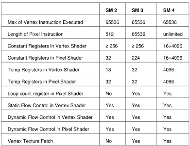
Table 2.1 Key specifications of Shader Models (SM)
SM 2 SM 3 SM 4
Max of Vertex Instruction Executed 65536 65536 65536
Length of Pixel Instruction 512 65536 unlimited
Constant Registers in Vertex Shader ≥ 256 ≥ 256 16×4096
Constant Registers in Pixel Shader 32 224 16×4096
Temp Registers in Vertex Shader 13 32 4096
Temp Registers in Pixel Shader 32 32 4096
Loop count register in Pixel Shader No Yes Yes
Static Flow Control in Vertex Shader Yes Yes Yes
Dynamic Flow Control in Vertex Shader Yes Yes Yes
Dynamic Flow Control in Pixel Shader Yes Yes Yes
Vertex Texture Fetch No Yes Yes
2.5 Languages for General-Purpose Computations
36
2.5.1 Brook for GPUs
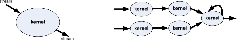
The Brook language from the Stanford University in USA is one of the first substantial efforts in simplifying GPGPU application development. It was initially designed primarily as a programming language for “streaming processors” (Dally et al., 2003). Buck et al. (2004) adapted Brook to harness the capabilities of computer graphics hardware; making it the first general-purpose language for the GPU (Buck et al., 2004). Brook extends the C programming language by inducing the concept of streams, a collection of elements, where each element will be manipulated by the same computations. Streams are different to arrays in conventional serial computing because there is no index operation and the element dependencies are forbidden. The functionality that is applied to each stream element is called a kernel, which is comparable to a “shader”.
The application development in Brook is a two-phase process; first the task is coded and compiled to a set of C++ files, and then the C++ files are loading and execution on the host machine. One major drawback of this approach is the target operating system, that is the graphics device specifications and the graphics API, has to be specified in advance.
2.5.2 CUDA – “Compute Unified Device Architecture”
Echoing the hardware architecture evolvement, Nvidia has devised a new generation parallel programming tool set. The Compute Unified Device Architecture (CUDA), enables simplifies the application development tasks to a C-programming job.
37
displaying computational results. The current CUDA version supports unique features such as branching, looping, pointers, large kernels, and multiple threads.
In addition to the intrinsic functions, the CUDA framework also includes extra utility libraries for operations such as linear algebra and the fast Fourier transform (FFT) that are important for applications like digital signal processing. The detailed programming specification in CUDA will be further discussed in Section 7.3 in combination with a case study.
With the release of the unified shader architecture and the CUDA-based computing model, data-parallel processing on GPU has extended from the earliest graphics applications to other scientific and engineering domains such as signal processing, physical simulation, computational biology and even computational finance.
2.5.3 CTM – “Close-to-the-Metal”
At about the same time of NVIDIA’s release of CUDA, its main market rival ATI (now part of the giant micro-processor manufacturer AMD) introduced the CTM platform -- a data-parallel virtual machine that allows direct communication with ATI graphics devices (Segal and Peercy, 2006). Similar to the CUDA architecture, many features are imposed by this approach, including the ability to read, modify, and write memory in a single program, to directly access host memory, or to cast between formats without explicitly copying the data. CTM is distributed as a library that allows “managed connections” to one of the three units of the graphics hardware to be opened, used, and closed: 1) The “command processor”, which is programmed via an architecturally independent language. 2) The “data-parallel processor” that is programmed via a native (architecturally dependent) instruction set. 3) The “memory controller” which allows direct access to the graphics and the main memory.
38
ordinary applications. Furthermore, a CTM application is responsible for all problems occurring at debugging, which increases the development complexity and cost.
2.6 Summary
Based on Leslie Lamport’s (Sinnen, 2007) definition, there are multiple levels at which parallelization can occur in a computational platform; the simplest micro-parallelization takes place inside a single processor and usually does not require the intervention of the programmer to implement. The so-called medium-grained parallelization for its intermediate repetitive core is normally associated with the host language’s semantics, and often appears in the form of advanced computational tasks, loop level parallelization. While efforts had been made in automating this level of parallelization with optimized compilers in the past, the results of those attempts were only of moderate success (Sinnen, 2007). For more advanced computational tasks, coarse-grain parallelization is often deployed which requires distributed memory parallel computers and are almost exclusively coded by the specially-trained programmer – not the application developers.
In practical engineering applications, there exist extensive specific processing procedures, such as reconfigurable computing and linear algebra matrix operations, which are implemented in specialized parallel devices, such as DSP, field programmable gate array (FPGA). Often, the key for the success of those devices is the cost, hence the invention of the term consumer-level or commodity-grade parallel processing. The majority of the attempts to date have focused on low-level data parallelism, but the recent trend has witnessed the interest shift to higher level parallelism, including instruction and task parallelism.
39
40
Chapter 3 General-Purpose Computing on
Graphics Card and Architectural Pattern
in Parallel Computing
GPU’s rapid evolution on its hardware design, coupled with the enhancing programmable capacity, has made GPGPU widely applicable in various domains of scientific computing, e.g., computational geometry, physically-based simulation, linear systems solution, partial differential equation, and database queries (Owens et al., 2007). Between 2001 and 2006, limited to the GPU pipeline structures that normally included vertex, rasterization, and pixel stages, the key GPGPU tasks had been focusing on how to efficiently implement an algorithm in the fixed rendering pipeline through mapping general-purpose computations to graphics hardware resources. Therefore, the key question to the GPGPU efforts was what types of computations map well to GPUs as briefly discussed in Chapter 2. Simply speaking, two key attributes of computer graphics computations, data parallelism and independence, will determine the outcomes and levels of success in a GPGPU application.
41
PC-grade parallel programming with this aim in mind. Based on these researches, four general classifications of parallel architectural pattern have been presented in this chapter, which are namely, divide and conquer, Pipes-and-Filters, communicating sequential elements, and processor farms.
3.1 Foundational Function Blocks: Streams and
Kernels
[image:62.595.124.513.560.629.2]For GPGPU applications, there are two essential components, stream and kernel, that distinguish data and instructions passed through the pipeline. A stream in GPGPU can be defined as the collection of data sets that need to be operated by the same computation. Multiple streams expose the so-called data parallelism due to the fact that all the data can be processed in parallel simultaneously. A kernel is the function or functions designed to perform the computations on each st