A Design Oriented Linear Model for CRLH Distributed Oscillators
Giancarlo Bartolucci1, *, Stefan Simion2, and Lucio Scucchia1
Abstract—The aim of this paper is to present a model for a Composite Right-/Left-Handed (CRLH) distributed oscillator. A linear approach is used for the analysis of the circuit. The effects of the losses and of the parasitic elements, both present in the active devices and in the passive components, are included. Analytic formulas for the design of the transmission lines used in the oscillator are given. The model is validated by means of a comparison with previously published measured data.
1. INTRODUCTION
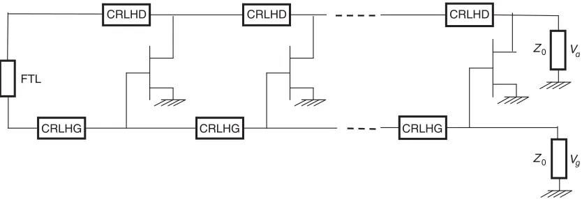
Distributed amplifier is an important wide-band element often used in microwave and millimeter wave systems [1–4]. The basic principle of this circuit has been also applied to other components, such as active dividers [5–7], frequency doublers [8–10], phase shifters [11–15], and oscillators [16–20]. For the latter ones the conventional configuration has been recently modified, replacing the low pass unit cell by a Composite Right-/Left-Handed (CRLH) topology [21, 22]. The conceptual configuration of this oscillator is shown in Fig. 1, where CRLHD and CRLHG are the drain and gate CRLH unit cells of the distributed amplifier, respectively. Each unit cell is composed by a series resonator and a parallel resonator, and for the transistor an ideal model can be assumed in this figure. Also, the drain and gate artificial lines of the distributed amplifier are connected by a feedback network (FTL) realized by means of a transmission line. As shown in [21], two output ports are available for this type of oscillator,
FTL
CRLHG CRLHG CRLHG
CRLHD CRLHD CRLHD
Z V
Z V
0
0 d
g
Figure 1. The distributed oscillator configuration composed by the feedback transmission line (FTL), the transistors, and the Composite Right-/Left-Handed cells termed CRLHD for the drain line and CRLHG for the gate line.
Received 22 May 2019, Accepted 18 July 2019, Scheduled 23 July 2019 * Corresponding author: Giancarlo Bartolucci ([email protected]).
1 Department of Electronic Engineering, University of Roma Tor Vergata, Via del Politecnico 1, Roma 00133, Italy. 2 Department
C
L
C G
Z
ic
ic
pic
ic
instubd
θ d, Zd
Figure 2. The unit cell of the drain line (CRLHD, taking into account the output impedance of the transistor).
Interdigital Capacitor
C
L
C G
Z
ic
ic
pic ic
instubg
θ g, Zg
Figure 3. The unit cell of the gate line (CRLHG, taking into account the input impedance of the transistor).
where similar power level may be obtained, with these output ports located at the ends of the drain and gate lines. In practice, CRLHD and CRLHG unit cells may be obtained using interdigital capacitors to realize the series resonators, while the parallel resonators are obtained using transmission lines, where the effects of parasitic capacitances of interdigital capacitors must be included. Taking into account the input and output equivalent circuits of the transistors, the circuit configurations for the CRLHD and CRLHG unit cells used in Fig. 1 behave more complicatedly, as shown in Fig. 2 and Fig. 3, respectively, where Cic, Lic, Cpic, Gic are elements of the interdigital capacitor equivalent circuit (here, the same for
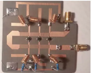
both unit cells). This oscillator has been designed and fabricated using MGF 4941AL InGaAs HEMTs, as presented in [21]. A photo of this circuit is presented in the same reference, but it is also shown here in Fig. 4 for the clarity of this paper, where the circuit elements of CRLHD and CRLHG unit cells may be observed.
Figure 4. Photograph of the fabricated CRLH distributed oscillator which uses three active devices (N = 3) [22].
C L
d Z , θ d
Id
d d Rd
Figure 5. The model of the part of the drain line unit cell included in the dotted rectangle in Fig. 2. It is composed by the equivalent circuit of the drain of the transistor and by the connecting line with lengthθd.
these effects, thus providing, in the general case, the analytic expression for the oscillation condition. Moreover, closed-form equations for the synthesis of the transmission lines utilized in the unit cell are derived.
The outline of the paper and the new contributions are listed below. In Sections 2 and 3 the models of the gate line and of the drain line are described, respectively. Section 4 is focused on the analysis of the feedback network, which is the key-element for transforming the distributed amplifier in an oscillator. Subsequently, the oscillation condition is imposed in the general case, including losses and parasitic effects. These analytic results are used in Section 5 for producing an innovative design procedure, which is the most important contribution of this work. In Section 6, some considerations on the power of the output signals are given. The validation of the presented approach is discussed in Section 7, where a comparison between predicted data and previously published experimental results is illustrated. Concluding remarks are provided in Section 8.
2. THE ANALYSIS OF THE DRAIN LINE
The equivalent circuit of the CRLHD unit cell is represented in Fig. 2. The transmission line of electrical length θd is used to facilitate the physical connection of the transistor drain, inside the drain unit cell.
The part of the cell included in the dotted rectangle is detailed in Fig. 5, where the equivalent circuit of the transistor drain together with the connecting transmission line is shown. This one port network can be characterized by means of the Norton’s theorem, so obtaining the equivalent circuit depicted in Fig. 6. For the admittanceYnd and the currentInd, we have:
Ynd =
1 Zd
Zd+jZLRCtgθd
ZLRC+jZdtgθd
(1)
and
Ind=
Id
P2cosθd
(2)
where:
ZLRC=jωLd+
Rd
1 +jωCdRd
(3)
and
P2 = 1 + (jωLd+jZdtgθd)
1 Rd
+jωCd
Ind Ynd
Figure 6. The Norton model for the circuit in Fig. 5.
Ind
Y
Ind
Ind
Pd YPd
YPd Vd
YLOAD
Figure 7. The equivalent network for the drain line.
Let’s assume that the circuit composed by the inductor Lic and the capacitor Cic resonates at the
oscillation frequency f0. Hence it becomes a short circuit, and according to Figs. 2, 5, and 6, the unit cell can be modeled by the current generator Ind and the admittanceYpd, which is defined as follows:
Ypd=Ynd+jω0Cpic+
1 Zinstubd
+Gic (5)
where Zinstubd is the input impedance of the stub in the drain unit cell. Therefore, at the frequency of resonance f0, for the whole drain line we can obtain the network shown in Fig. 7. The admittance YLOADis obtained by adding the load admittance of the drain line, that is 1/Z0, to the input admittance of the feedback network loaded by the gate line.
3. THE ANALYSIS OF THE GATE LINE
The equivalent circuit of the CRLHG unit cell is shown in Fig. 3. The transmission line of electrical length θg has a similar role to the line of electrical length θd used in the drain unit cell. It must be
mentioned that the lines of electrical lengths θg and θd also ensure a separation between the gate and
Cg Vg
Rg
Lg
Vgk Zg
θg Ygin
Figure 8. The model of the part of the gate line unit cell included in the dotted rectangle in Fig. 3. It is composed by the equivalent circuit of the gate of the transistor and by the connecting line with length θg.
Fig. 2). The differences are in the value of the input impedance of the stub and in the electric parameters of the connecting line. The model of the elements included in the dotted rectangle is shown in Fig. 8, where the equivalent circuit of the transistor gate and the connecting line are present. For the input admittance Ygin we find:
Ygin=
Zg
Zgk+jZgtgθg
Zg+jZgktgθg −1
(6)
whereZgk is given by:
Zgk =jωLg+
1 jωCg
+Rg (7)
The following relationship between Vgk and Vg can be written:
VgK =P4Vg (8)
where:
P4=
1
jωCg(Zgkcosθg+jZgsinθg)
=|P4|ejψ4 (9)
As for the drain line, the unit cell of the gate line is characterized by an admittanceYpg, which is defined
at f0 as:
Ypg=Ygin+jω0Cpic+
1 Zinstubg
+Gic (10)
whereZinstubg is the input impedance of the stub in the gate line unit cell.
4. THE FEEDBACK NETWORK AND THE OSCILLATION CONDITION
A transmission line with characteristic impedanceZ0 and electric lengthφ0, evaluated atf0, is used for realizing the feedback network (see Fig. 1). IfN is the number of unit cells, the load admittance of this feedback line, let sayYLg, is given by the load impedance of the gate line Z0 and by the admittances of theN cells, and the resulting circuit may be used to compute the input admittance into the feedback line,Ydi, given in Fig. 9. Thus, we have the following expression forYLg andYdi:
YLg =
1 Z0
" "
Vd
di Z 0, φ
Vg NYPg Z0
Figure 9. The feedback transmission line loaded byZ0 and by the N gate line unit cells.
and
Ydi=
Z0
1 +jYLgZ0tgφ Z0YLg+jtgφ
−1
(12)
The relationship between Vg and Vdcan be expressed as:
Vg =Vd(cosφ−jZoYdisinφ) (13)
Vd can be calculated as the ratio of the current given by the N generators Ind and the admittance
obtained by adding YLOAD to NYpd. Therefore:
Vd= −
NInd
NYpd+YLOAD
= −N
NYpd+YLOAD Id
P2cosθd
(14)
where:
YLOAD= 1 Zo
+Ydi (15)
We assume for Id:
Id=gmVgK =gmP4Vg (16)
By substituting Equation (16) in Equation (14), we obtain:
Vd= −
N NYpd+YLOAD
gmP4Vg
P2cosθd
(17)
From Eqs. (17) and (13) one then has:
1 = −NgmP4 P2cosθd
(cosφ−jZoYdisinφ)
NYpd+YLOAD
(18)
This equation is the oscillation condition for the CRLH distributed oscillator.
5. THE DESIGN PROCEDURE OF THE CRLH OSCILLATOR
We can note that neglecting the losses in the two stubs, their input impedances Zinstubd and Zinstubg are imaginary numbers. By using Equations (5) and (10), let us impose the following conditions at the oscillation frequency f0:
jIm [Ypd] = jIm [Ynd] +jω0Cpic+
1 Zinstubd
= 0 (19)
jIm [Ypg] = jIm [Ygin] +jω0Cpic+
1 Zinstubg
= 0 (20)
Equations (19) and (20) can provide the values ofZinstubd andZinstubg, thus allowing the design of the two stubs. As a consequence of Eqs. (19) and (20), the admittances Ypd,Ypgare real and become:
Ypd = Re [Ynd] +Gic (21)
Let’s introduce parameters B,D,ψ:
B = Z0NYpg (23)
D =
[NYpd+ (2 +B)Yo]2+NYpdB[(2 +B) (NYpd+ 2Yo)] sinφ2 (24)
ψ = arctg
tgφ(1 +B) (NYpd+Yo) +Yo NYpd+ (2 +B)Yo
(25)
so that the oscillation condition (18) can be written as:
1 = −Ngm|P4|e
jψ4
Dejψ|P2|ejψ2cosθd (26)
which gives:
ψ=−ψ2+ψ4+π (27)
and
gm =
D|P2|cosθd
N|P4| (28)
According to Eq. (25), the unknownφis related to the phase ψ as follows:
φ= arctg
tgψ NYpd+ (2 +B)Yo (1 +B) (NYpd+Yo) +Yo
(29)
The phase φmust be inserted in Eq. (24) for obtainingD, which in turn can be utilized in Eq. (28) for computinggm.
In conclusion, the design steps of the distributed oscillator can be briefly summarized as follows: Step1: The interdigital capacitor is designed by means of an electromagnetic simulator, imposing f0 as resonance frequency. Hence, the values of the capacitance Cpic and of the conductance Gic are
also calculated.
Step2: The two transmission lines used for connecting the transistor to the passive elements of the unit cells are synthesized, choosing the electric lengths θd and θg in such a way to avoid unwanted
coupling effects between the gate and drain lines.
Step3: The bias point in the characteristic curves of the transistor is selected. As a consequence of this choice, the values of Ld,Lg,Cd,Cg,Rd, and Rg are obtained.
Step4: The two stubs are designed by using the values ofZinstubdandZinstubgprovided by Eqs. (19) and (20).
Step5: The electric length φ is utilized for computing the geometric length of the feedback transmission line.
6. CONSIDERATIONS ON THE POWER OF THE OUTPUT SIGNALS
The distributed oscillator shown in Fig. 1 has two output ports, hence it provides two sinusoidal signals. The linear model presented in this paper does not allow to calculate the powers of these signals, respectivelyPg andPd. However, it yields an analytic formula for the ratio of these two powers,
which is related to the difference between their values in dBm, PgdBm and PddBm. The expressions of PgdBm and PddBm can be written as:
PgdBm = 10 logPg = 10 log |
Vg|2
2Z010−3 (30)
PddBm = 10 logPd= 10 log |
Vd|2
2Z010−3 (31)
Thus we have for the difference of the output powers ΔPdBm:
ΔPdBm=PddBm−PgdBm= 10 log| Vd|2
|Vg|2
From Eqs. (32) and (33), we obtain for ΔPdBm:
ΔPdBm= 10 log| Vd|2
|Vg|2
= 10 log1 + sinφ2(2 +B)B (34)
7. COMPARISON WITH EXPERIMENTAL RESULTS
The numerical results obtained by using the proposed linear approach have been compared to the experimental results presented in [22]. The values of its equivalent circuit elements are listed in Table 1. In particular, Ld, Lg, Cd, Cg, and Rg have been obtained in [23], whereas Rd is as usual computed
as the inverse of the slope of the current-voltage characteristics (Id-Vd) at the operating point. In
Table 1, the values of Cpic and Gic are also reported, both achieved by the electromagnetic simulation
of the interdigital capacitor. For this purpose, the Momentum simulator implemented in the Advanced Design System (ADS) — Keysight software package has been utilized. Moreover, in Table 1 the values of characteristic impedances Zd, Zg and the values of electrical lengths θd and θg are given. For this
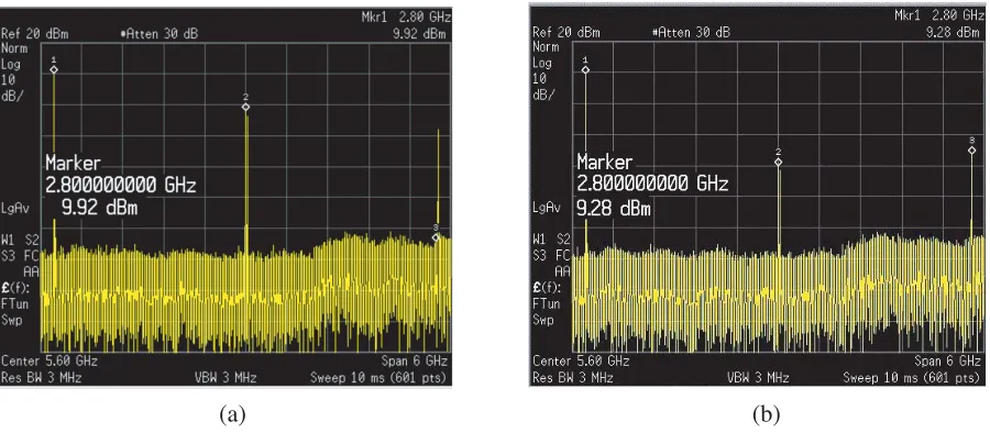
oscillator, the measured frequency spectra at the drain and gate line outputs are presented in Fig. 10 [22]. Using these experimental results, ΔPdBm= 0.64 dBm is obtained. In Table 2, the values for ΔPdBmand φ(evaluated at the oscillation frequency f0 = 2.8 GHz) are computed by using the formulas developed in this paper, in comparison with the results provided by the simplified analysis [21] and with the experimental values measured for the realized circuit [22]. From Table 2, the following considerations can be inferred:
• The length of the feedback line for the manufactured oscillator is smaller than the value predicted in [21]. The proposed approach yields an electric length quite close to the value of the realized circuit.
• By using the simplified analysis in [21], the same power is expected for the two output signals. However, the measured values are not equal. This difference is mostly accounted in the described model. It is worth adding that in the model the losses in the feedback line and the stubs are not included. This approximation can explain the existing small discrepancy in Table 2.
(a) (b)
Table 1.
Parameters Values
Ld (nH) 1
Lg (nH) 0.45
Cd(pF) 0.16
Cg (pF) 0.43
Rd (Ω) 250
Rg (Ω) 18
Cpic (pF) 0.64
Gic (Ω−1) 0.733·10−3
Zd (Ω) 107
Zg (Ω) 107
θd (◦) 18.6
θg (◦) 6.2
Table 2.
Parameters φ(deg.) ΔPdBm Simplified analysis [21] 180◦ 0
Realized Circuit [22] 138◦ 0.64
This work 158◦ 0.41
8. CONCLUSION
A linear model for the CRLH distributed oscillator has been proposed. An analytic expression for the oscillation condition has been obtained. The model includes most of the losses present in the structure. Moreover, it provides a general design procedure for this kind of circuit. A comparison with experimental results for a previously realized oscillator confirms the validity of the presented approach.
REFERENCES
1. Lin, Y.-S., J.-F. Chang, and S.-S. Lu, “Analysis and design of CMOS distributed amplifier using inductively peaking cascaded gain cell for UWB systems,”IEEE Trans. Microwave Theory Techn., Vol. 59, No. 10, 2513–2524, 2011.
2. Entesari, K., A. R. Tavakoli, and A. Helmy, “CMOS distributed amplifiers with extended flat bandwidth and improved input matching using gate line with coupled inductors,” IEEE Trans. Microwave Theory Techn., Vol. 57, No. 12, 2862–2871, 2009.
3. Bartolucci, G., F. Giannini, and L. Scucchia, “Design considerations for the gate circuit in distributed amplifiers,”IET Circuits Devices Systems, Vol. 4, No. 3, 181–187, 2010.
4. Guan, X. and C. Nguyen, “Low-power-consumption and high-gain CMOS distributed amplifiers using cascade of inductively coupled common-source gain cells for UWB systems,” IEEE Trans. Microwave Theory Techn., Vol. 54, No. 8, 3278–3283, 2006.
5. Lo, W. K. and W. S. Chan, “Broadband integrated active divider and combiner based on distributed amplification,” Electronics Letters, Vol. 44, No. 13, 779–780, 2008.
8. Carman, E., M. Case, M. Kamegawa, R. Yu, K. Giboney, and M. J. W. Rodwell, “V-band and W-band broadband, monolithic distributed frequency multipliers,”IEEE Microwave Guided Wave Lett., Vol. 2, 253–254, 1992.
9. Tang, Y. L., P.-Y. Chen, and H. Wang, “A broadband PHEMT MMIC distributed doubler using high-pass drain line topology,” IEEE Microwave and Wireless Components Lett., Vol. 14, No. 5, 201–203, May 2004.
10. Simion, S. and G. Bartolucci, “Distributed amplifier based broadband and low spurious frequency doubler,”Romanian Journal of Information Science and Technology, Vol. 20, No. 4, 331–341, 2017. 11. Hung, J. J., L. Dussopt, and G. M. Rebeiz, “Distributed 2- and 3-bit W-band MEMS phase shifters
on glass substrates,”IEEE Trans. Microwave Theory Techn., Vol. 52, No. 2, 600–606, 2004. 12. Bartolucci, G., “Image parameter modeling of analog traveling-wave phase shifters,” IEEE
Transactions on Circuits and Systems I: Fundamental Theory and Applications, Vol. 49, No. 10, 1505–1509, 2002.
13. Topali, K., O. A. Civi, S. Demir, S. Koc, and T. Akin, “A monolithic phased array using 3-bit distributed RF MEMS phase shifters,” IEEE Trans. Microwave Theory Techn., Vol. 56, No. 2, 270–277, 2008.
14. Du, Y., J. Bao, and X. Zhao, “5-bit MEMS distributed phase shifter,”Electronics Letters, Vol. 46, No. 21, 1452–1453, 2010.
15. Bartolucci, G., S. Catoni, F. Giacomozzi, R. Marcelli, B. Margesin, and D. Pochesci, “Realisation of distributed RF MEMS phase shifter with very low number of switches,” Electronics Letters, Vol. 43, No. 23, 1290–1292, 2007.
16. Skvor, Z., S. R. Saunders, and C. S. Aitchison, “Novel decade electronically tunable microwave oscillator based on the distributed amplifier,”Electronics Letters, Vol. 28, No. 17, 1647–1648, 1992. 17. Divina, L. and Z. Skvor, “The distributed oscillator at 4 GHz,” IEEE Trans. Microwave Theory
Techn., Vol. 46, No. 12, 2240–2243, 1998.
18. Wu, H. and A. Hajimiri, “Silicon-based distributed voltage-controlled oscillators,” IEEE Journal of Solid-State Circuits, Vol. 36, No. 3, 493–502, 2001.
19. Aku, M. O. and R. S. Imam, “Silicon bipolar distributed oscillator design and analysis,” Science World Journal, Vol. 9, No. 4, 29–38, 2014.
20. Bhattacharyya, K., “Tunable distributed harmonic voltage controlled oscillator for generating second and third harmonic microwave signals in 180 nm CMOS,” International Conference on VLSI Systems, Architectures, Technology and Applications (VLSI-SATA), 1–4, 2016.
21. Simion, S. and G. Bartolucci, “High power efficiency distributed oscillator based on composite-right-/left-handed unit cells,” Appl. Phys. Lett., Vol. 107, 104102, 2015.
22. Bartolucci, G., S. Simion, and L. Scucchia, “Power performance and spurious frequencies analysis of composite right-/left-handed (CRLH) distributed oscillators,” Progress In Electromagnetics Research Letters, Vol. 75, 67–73, 2018.