Fuzzy Control Based High Voltage Gain
Step-Up Converter Combining KY and Buck-Boost
Converters
Anju
1, Rabiya Rasheed
2PG Student [PEPS], Dept. of EEE, Federal Institute of Science and Technology, Angamaly, Kerala, India1
Assistant Professor, Dept. of EEE, Federal Institute of Science and Technology, Angamaly, Kerala, India2
ABSTRACT: This paper presents a voltage boosting converter with a control circuit of fuzzy logic controller. Converter combines one KY converter, one traditional synchronously rectified (SR) buck-boost converter, and one coupled inductor with the turns ratio, which is used to improve the voltage gain. Thus, the voltage gain is higher than the previous converters. Analog input values are analyzed using the fuzzy logic controller in terms of logical variables and takes continuous values between 0 and 1. Output voltage, rise time, peak time and settling time of the response are neatly controlled by fuzzy controller circuit. Also, it maintains the output voltage constant when subjected to heavy load changes and input voltage changes. In this paper, performance analysis between the PI controller and the fuzzy logic controller has been compared based on different loads. The model is developed in MATLAB/Simulink. Simulink input voltage was set at 12V and the output voltage obtained is 72V.
KEYWORDS: KY converter, coupled inductor, synchronous rectification (SR), fuzzy logic controller.
I.INTRODUCTION
The portable electronics industry has been progressed widely over the years. Increased battery life, cheap systems, colored displays, etc such lot of requirements also evolved. Demands from the power systems as well as the demand for green power have been increasing for decades. In order to keep up with these demands, engineers greatly worked towards developing efficient and compatible conversion techniques. High voltage conversion converters are used for boosting voltage as per the requirement of load. When control techniques are applied to these converters, it produces the output more efficiently as compared to the converter when used in open loop. Therefore, effective methods are employed to design the control systems. In this paper, it proposes fuzzy logic controller which is a non linear controller. The non linear phenomenon occurring in the converter can be easily tackled using the fuzzy logic controller. Thus, it provides output which has lower rise time, peak time and settling time.
In this paper, the power circuit of the converter mainly consist of KY converter, one traditional SR buck-boost converter, and one coupled inductor. Basically the coupled inductor is used as the voltage gain enhancement technique which is one of the most efficient techniques. Moreover the proposed converter has an output inductor, which makes it output current non-pulsating. As said above, the control circuit of the converter is designed using the fuzzy logic controller in which the input voltage is traced by the output voltage.
II.LITERATURE SURVEY
ISSN (Print) : 2320 – 3765 ISSN (Online): 2278 – 8875
I
nternational
J
ournal of
A
dvanced
R
esearch in
E
lectrical,
E
lectronics and
I
nstrumentation
E
ngineering
(An ISO 3297: 2007 Certified Organization) Vol. 4, Issue 10, October 2015
Use of coupled inductor gives low output voltage ripples but it has certain limitations. To overcome its limitations, a new voltage boosting converter named KY converter was used [1]-[2]. KY converter is a boost converter that operates always in continuous conduction mode (CCM). This converter has good load transient response. But its voltage gain is not so high. A step-up converter combining KY and buck-boost converter came up which could extend the voltage conversion ratio of the KY converter [3]-[4]. It had low voltage ripples. Since the converter possessed an output inductor, non-pulsating current was flowing through the output capacitor.
In order to further increase the voltage gain, another new step-up converter combining KY converter, synchronously rectified (SR) buck-boost converter and one coupled inductor came up [5]. This converter gave improved voltage gain than the other conventional converters but the limitation faced by this converter is its non linear performance, i.e., the settling time was very high and also the output voltage fluctuations were large when subjected to any change in load or change in the input voltage. In order to lower the settling time and improve the performance of the converter, the control circuit is designed with fuzzy logic controller.
This paper shows the operational principles and simulation results of the proposed converter. In section III structure and operational principle of the proposed converter is explained. In section IV fuzzy logic control of the converter is explained. In section V simulation results obtained by implementing fuzzy logic controller is presented and the conclusion is presented in section VI.
III.STRUCTURE AND OPERATIONAL PRINCIPLE
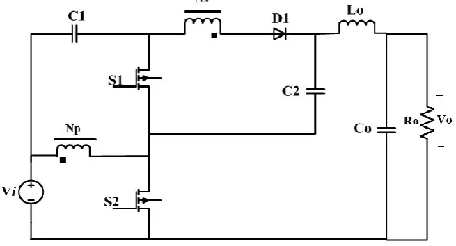
The proposed converter is shown in fig. 1. The converter contains two MOSFET switches S1 and S2, one coupled inductor composed of the primary winding with Np turns and the secondary winding with Ns turns, one energy-transferring capacitor C1, one charge pump capacitor C2, one diode D1,one output inductor Lo, one output capacitor Co. In addition, input voltage is signified by Vi, the output voltage is denoted by Vo and the output resistor is represented by Ro.
Fig. 1 Proposed Converter
Mode 1:
Fig 2 Mode 1 operation of the converter
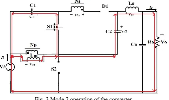
Mode 2:
Figure 3 shows the mode 2 operation of the proposed converter. In this mode, S1 is turned on and S2 is turned off. Thus, voltage imposed on Np is –VC1. Hereby, Lm gets demagnetized and the voltage across Ns is equal to –VC1 × Ns/Np. Thus, the diode D1 become reverse biased. The voltage across Lo is a positive value and is equal to Vi + VC1 + VC2 – Vo, thus causing Lo to be magnetized. Therefore, voltage across Lm plus the voltage across C2 provides energy to the load.
Fig. 3 Mode 2 operation of the converter
IV.FUZZY LOGIC CONTROL OF THE CONVERTER
ISSN (Print) : 2320 – 3765 ISSN (Online): 2278 – 8875
I
nternational
J
ournal of
A
dvanced
R
esearch in
E
lectrical,
E
lectronics and
I
nstrumentation
E
ngineering
(An ISO 3297: 2007 Certified Organization) Vol. 4, Issue 10, October 2015
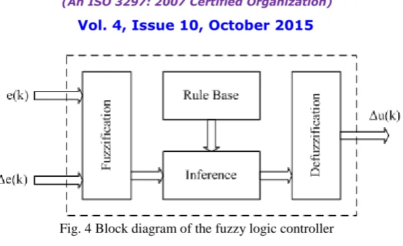
Fig. 4 Block diagram of the fuzzy logic controller
The input stage of the controller senses the input and selects the appropriate membership functions and truth values. In the processing stage, rules are evaluated and the results are generated. And finally, in the output stage fuzzy sets are converted back to crisp values and provide the output. The fuzzy sets are converted to crisp values by the help of Defuzzification block of the controller. Here, the centroid method is being used as the defuzzification technique. The error is reduced using this closed loop control. Here, fuzzy logic controller employs 9 rules. If error is negative and error change is negative, then output is decrease. If error is negative and error change is zero, then output is decrease. If error is negative and error change is positive, then output is decrease. If error is zero and error change is negative, then output is decrease. If error is zero and error change is zero, then output is no change. If error is zero and error change is positive, then output is increase. If error is positive and error change is negative, then output is increase. If error is positive and error change is zero then output is increase. If error is positive and error change is positive, then output is increase. Likewise, output follows the input and doesn’t make significant changes when subjected to load change.
V. SIMULATION RESULT
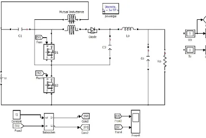
Figure 5 show the simulation model of the converter with the control circuit designed using fuzzy logic controller is used. For an input voltage of 12V, the output voltage obtained is 72V. The switching frequency provided is 100kHz and turns ratio for the coupled inductor taken is 1:3. The value for the magnetizing inductor Lm used is 149µH. Output inductor Lo is taken 180µH and the capacitor values C1 and C2 are 174µF and 69.4µF respectively. In the simulation block, the coupled inductor is provided with a mutual inductance block in which the L1 value is same as the magnetizing inductance value and the L2 value is provided by the formula L1 × (N1/N2)2. The mutual inductance value is given by the formula, k × (L1 × L2)0.5. The value of coupling coefficient (k) is taken to be 1 because the leakage inductance is omitted. Duty cycle for the switch S1 is D and for S2 is 1-D. Here, the duty cycle D is taken to be aprrox. 0.5.
Fig. 5 Simulation diagram of the proposed converter
Fig. 6 Control block of the converter
ISSN (Print) : 2320 – 3765 ISSN (Online): 2278 – 8875
I
nternational
J
ournal of
A
dvanced
R
esearch in
E
lectrical,
E
lectronics and
I
nstrumentation
E
ngineering
(An ISO 3297: 2007 Certified Organization) Vol. 4, Issue 10, October 2015
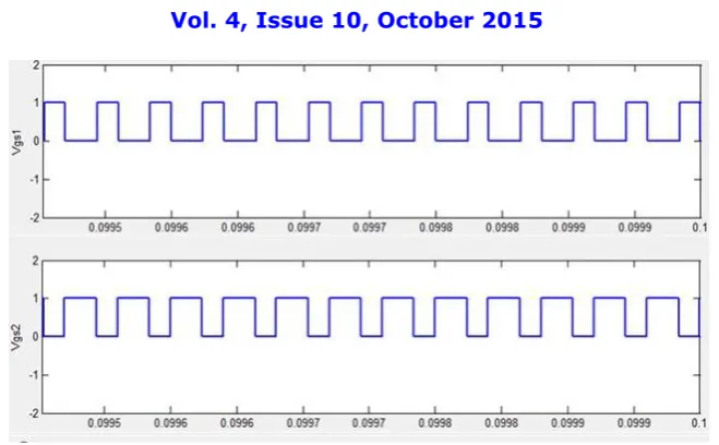
Fig. 7 Gate pulses across the switches S1 and S2.
Fig. 8 Voltage across the output inductor
Fig. 10 Output voltage waveform of the converter
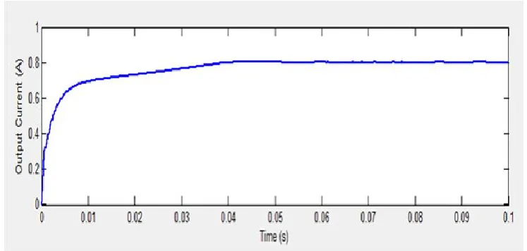
Fig. 11 Output current waveform of the converter
VI.CONCLUSION
A fuzzy based control step up converter for voltage gain enhancement has been presented herein. The simulation of the proposed converter is presented and explained. The control is provided with fuzzy logic controller to get efficient performance of the converter. Not only the voltage gain is enhanced but also the output voltage fluctuations are reduced to its maximum level and the nonlinear performance of the converter is reduced. For an input voltage of 12V, the output voltage of 72V is obtained. Moreover of the structure of the proposed converter sis simple and also the control part i.e., fuzzy logic controller is also simple and very well suitable for the industrial applications.
REFERENCES
[1] K. I. Hwu and Y. T. Yau, “KY converter and its derivatives,” IEEE Trans. Power Electron., vol. 24, no. 1, pp. 128–137, Jan. 2009. [2]. K. I. Hwu and Y. T. Yau, “A KY boost converter,” IEEE Trans. Power Electron., vol. 25, no. 11, pp. 2699–2703, Nov. 2010.
[3]. K. I. Hwu, K. W. Huang, and W. C. Tu, “Step-up converter combining KY and buck-boost converters,” IET Electron. Lett., vol. 47, no. 12, pp. 722–724, Jun. 2011.
[4]. K. I. Hwu and Y. T. Yau, “Inductor-coupled KY boost converter,” IET Electron. Lett., vol. 46, no. 24, pp. 1624–1626, Nov. 2010.