UNIVERSITY OF LEIDEN
Fabrication of Single Electron Charging
Devices for Optical Charge Sensing
Experiments
by
Robert Smit
A thesis submitted in partial fulfillment for the degree of Master of Science
in the Faculty of Physics
MoNoS
Supervisor: prof. dr. M. Orrit and dr. S. Faez
UNIVERSITY OF LEIDEN
Abstract
Faculty of Physics
MoNoS
by Robert Smit
To sense the movement or piling up of single charges, a system interacting strongly with
these charges is required. An available system, having these properties, is a single electron
transistor (SET). The electric field caused by the charge, strongly changes the resistance
of the SET. Yet experiments opt for a less invasive charge sensor. Such a proposed charge
sensor is a single fluorescent dye molecule. The distinguishable zero phonon lines (ZPL’s)
of the fluorescence of the molecules shifts strongly by the Stark effect. The lineshift of each
molecule can be tracked with an excitation laser, allowing to observe the change in charging.
Tracking the ZPL’s of multiple molecules allows the observation of slow charge movement.
The optical charge sensing method needs to be tested on devices fabricated on a glass
sub-strate. In particular devices, which exhibit single electron charging. These devices have been
constructed with electron beam lithography (EBL). Nanoparticles, representing an island
to hold the charge, have been trapped between nano-electrodes using dielectrophoresis. The
nanogaps have been created by electromigration or by EBL. Eventually, nano-electrodes were
also fabricated on glass by coating the glass with a 1,5 nm Cr layer. This coating was removed
afterwards with plasma etching. The project focused on the fabrication of the devices. The
deposition of fluorescent dye molecules and tracking the lineshifts was left for subsequent
experiments. A fluorescence microscope, also necessary for the lineshift measurements, was
used to observe quantum dots. Proposed experiments with quantum dots are the tracking
of the movement of quantum dots in a strong alternating electric field or the effect of a high
Acknowledgements
I hereby want to thank my supervisor, dr. S. Faez, for guiding me during this research
project. We had interesting discussions in which I learned much about optics. I also want
to thank the people in the Single Molecule Optics Group. I enjoyed discussing the latest
research in our field with them. We had lively discussions, in general during the group
meetings, which were a good source for inspiration for my own project.
Additionally, i want to thank the groups on the 7th floor, which are part of the condensed
matter department. They guided me through the fabrication process and allowed me access
to their facilities for nanofabrication. In special, I want to thank Msc. S. Blok. He helped
me a lot with electron beam lithography and the creation of nanoparticles. The latter was
done in cooperation with Msc. E. Devid. The dissertation of dr. P. Navarro was a source
of inspiration for writing my own thesis. I thank him for giving it to me and also for the
theoretical discussions we had. Finally, I want to thank my girlfriend Rolinde for her feedback
on my writings.
Contents
Abstract i
Acknowledgements ii
1 Theory of Single Electron Charging 1
1.1 Single Charge Sensing . . . 1
1.1.1 Optical Charge Sensing . . . 1
1.2 Single Electron Charging. . . 2
1.3 The Single Electron Transistor . . . 4
1.4 Scaling Down: From Nanoparticle to Quantum Dot . . . 6
1.5 Optically Measuring a Moving Charge . . . 7
2 Experimental Methods 9 2.1 Electron Beam Lithography . . . 9
2.1.1 The Scanning Electron Microscope . . . 9
2.1.2 From SEM to EBPG . . . 12
2.1.3 Proximity effect. . . 14
2.2 Fabricating Single Electron Devices. . . 15
2.2.1 Electrodes with Nanometer Seperation . . . 15
2.2.2 Electromigration . . . 16
2.3 The Nanoparticle Island . . . 18
2.3.1 Dielectrophoretic Trapping of Nanoparticles . . . 18
2.3.2 Coating the Gold Nanoparticles . . . 20
2.4 Optical Experiments . . . 21
2.4.1 Electron Beam Lithography on a Glass Substrate . . . 21
2.4.2 Fluorescence Microscope . . . 22
3 Experimental Results 24 3.1 Building Single Electron Devices . . . 24
3.1.1 Creating Nano-Electrodes . . . 24
3.1.2 Nanoparticle Trapping in an EBL defined gap . . . 26
3.1.3 Gap Creation by Electromigration . . . 28
3.1.4 Parallel Electrodes . . . 29
3.2 Electron Beam Lithograhy on Glass as a Substrate . . . 30
3.3 Observing Single Quantum Dots . . . 32
Contents iv
4 Discussion and Prospects 34
4.1 The Purpose . . . 34
4.2 Single Electron Charging Devices . . . 34
4.3 Fabrication on a Glass Substrate . . . 35
4.4 Quantum Dot Experiments . . . 35
Chapter 1
Theory of Single Electron Charging
1.1
Single Charge Sensing
The measurement of charge movement, or current, is a common practise in experimental
physics. However, this measurement comprises a net sum of the charges moving in opposite
directions as predicted by quantum mechanics. The current sensors are also very limited
in their sensitivity. Eventually, when the current is decreased, charge movement becomes
quantized by the discreteness of the electrons. To measure the movement of discrete charges,
a far more sensitive charge sensor has to be fabricated and in general has to be embedded
into the system to be measured. A lot more insight into systems studied nowadays can be
gained by being able to measure the movement of single charges. This has been achieved
before. For example, single electron charging on a 2DEG quantum dot has been measured
with a single electron transistor (SET) in its vicinity [1]. Due to the capacitive coupling of the quantum dot with the island of the SET, the current flow through the SET was strongly
modulated by the amount of charge on the quantum dot. Unfortunately, the SET had to
be fabricated next to the quantum point contacts of the quantum dot. Another example
involved graphene. This very promising material shows limited conductivity when it has
been deposited on a substrate. This is explained by the trapping of charges in puddles.
These trapped charges have been measured as well, using the charge sensitivity of the SET
[2].
1.1.1 Optical Charge Sensing
A promising technique, that doesn’t require elaborate fabrication steps and therefore is also
less invasive to the system under study, is the use of single molecule probes [3]. Theoretical studies have shown that the electron charge sensitivity of some single molecules with large
Chapter 1. Theory of Single Electron Charging 2
dipole moments between the ground and excited state could easily surpass 10−5 e/√Hz[4]. This charge sensitivity is comparable to what is obtained with a SET [1]. The single molecule probe is a fluorescent dye with a distinguishable zero phonon line (ZPL) in the emission
spectrum. These fluorescent dyes are embedded in a crystalline structure (host) in a very
low concentration of nM’s. Because, the electron-phonon coupling between the host and
dye is very weak, the phonon side-band of the molecule’s emission spectrum is much less
pronounced than the ZPL. The ZPL of the dye can be shifted strongly in the presence of
an electric field and this can be measured by tuning the narrow bandwith excitation laser
to the new resonance frequency. Therefore, the Stark shift needs to be at least a few times
larger than the bandwith of the laser. To obtain a seperation between the zero phonon lines
of all the molecules, impurities can be added into the host to change the environment of
each molecule. The different environment causes different perturbations in the Hamiltonian
of the molecules. Therefore, the lines will shift to distinctual frequencies and will form a
discrete spectrum of ZPL’s. By scanning the laser’s frequency over a broad range, covering
the discrete spectrum of ZPL’s, each molecule can be excited at its resonance frequency. By
mapping the position of the fluorescence, a spot will appear at the position of the molecule,
whenever the laser’s frequency is in resonance with the two level system of the molecule.
In this research project, the main focus was to fabricate the devices, which can exhibit single
electron or few electron charging and are compatible with optics. It is important for the
experiment that the laser light has to pass through the sample. Therefore, the substrate has
to be transparent for the fluorescence light. Methods for fabrication of nanoscale structures
on glass substrates have been undertaken. And additionally, the creation of structures that
meant to exhibit single electron charging, such as SET’s and the single electron box. The
theoretical description of the SET and single electron box are explained extensively in the
next section. The theory of charge sensing with single molecule probes is not covered in detail,
because this was also not part of the experiment. This is left for subsequent experiments.
1.2
Single Electron Charging
A simple case of single electron charging is the well known single electron box. The single
electron box is a small island seperated from an electron reservoir by a tunnel junction. It is
well known that, to charge an object, the repulsive Coulomb force of the electrons has to be
bypassed. This will cost energy, which is given by the electrostatic energy equation:
E = Q
2
Chapter 1. Theory of Single Electron Charging 3
Here, Q represents the total amount of charge to be moved; in this particular case to the
island. Furthermore, C is the self capacitance of this island. Scaling down the size of the
island would decrease it’s self-capacitance and as there is an inverse relationship with the
electrostatic energy, C would increase. When Q is substituted for the charge of a single
electron, namely e=1,602.10−19C, then E is the so called charging energy of a single electron.
If the shape of the island is spherical, the self- capacitance can be approximated by:
CΣ =
Q
∆V =
1 4π0r
Z ∞
R
1
r2dr
−1
= 4π0rR (1.2)
Therefore, the only important factors that change the self-capacitance, are the dielectric
constant of the island and it’s size. A schematic configuration of the single electron box is
shown in figure 1.1. On the right are depicted the chemical potentials. The discrete energy
level distribution of the island is caused by the quantization of the charging state. If, in
this specific case the (N+1)-th electrode is not occupied, it will likely remain so when two
conditions are satisfied. The first condition is related to the Fermi-Dirac distribution of the
electron energy states. The electron states above the Fermi energy, in a range of the thermal
energy kbT, are partly occupied. Therefore, at finite temperature, there might be electrons
with large enough energy to bypass the Coulomb barrier. A Coulomb barrier, much larger
than the thermal energy, would avoid crossing. Hence, the condition e2/2C k
bT, must be
satisfied.
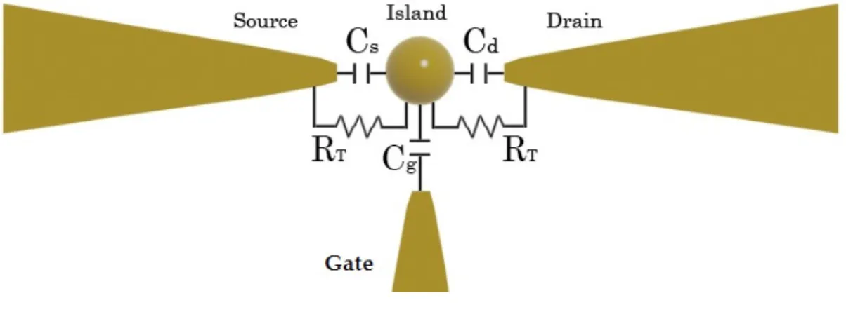
Figure 1.1: (a) Schematic of the single electron box. The source electrode is capacitively
coupled to the island with capacitance Cg. In between is also a tunnel junction of resistance
RT and the island has a self capacitance CΣ. (b) The same system is depicted in terms of
chemical potentials. If there are N electrons on the island, an additional electron can tunnel from the source electrode to the island, whenf + eV≥µN+1.
A second important condition concerns the size of the tunneling barrier. Charges from the
island can leak to the electrodes through the tunneling barrier with a characteristic time
Chapter 1. Theory of Single Electron Charging 4
electrons. This would allow the electron to gain an increase in energy, which is higher than
the charging energy. Therefore, required is that ∆E e2/2C or:
~
τ =
~
RC e2
2C =⇒
~
R e2
2 =⇒R
h
2e2 =Rq (1.3)
This means that the tunneling barriers will have to be much larger than the quantum value
of resistance. The first condition requires that the sample has to be cooled down to lower
temperatures. At room temperature, the thermal energy is already 25.6 meV. A 10 nm sized
spherical island will have a self capacitance of 77 meV, but creating such an island is already
difficult. When the sample is cooled down to 4,2 K, the thermal energy is reduced to 0,35
meV. Coulomb blockade becomes much more efficient when the sample is cooled down.
1.3
The Single Electron Transistor
Figure 1.2: Schematic of a symmetric SET. When the shapes of both electrodes are equal,
then Cs=Cd. The source and drain electrodes are connected to a voltage source to peform
transport measurements.
A second electrode added to the single electron box structure completes the single electron
transistor (SET). The second electrode will serve as a drain. Coulomb theory of a single
electron box already existed in 1969 when it was formulated by Zeller and Giaver for small
particles embedded in tunneling barriers [5]. Though, it would still take 18 years before the discovery of the SET by Fulton and Dolan[6]. Since then many research has been conducted on the device, but the working principle remained the same.
For the theoretical description, it is assumed that the tunneling barriers are symmetric for the
source-particle and particle-drain barriers. To tunnel an electron from the source electrode
to the island, the Coulomb barrier has to be bypassed. Because, the SET both contains a
source and drain electrode, transport measurements can be undertaken. When the voltage
on the source electrode is equal to e/2C, the voltage drop between the source and particle is
Chapter 1. Theory of Single Electron Charging 5
which contains twice the charging energy, allows the transport. Therefore, current movement
in the SET, is blocked in the range of [-e/C , e/C]. From the IV curve, the charging energy
can be deduced. An example of such a transport measurement is given in figure 1.3.
Figure 1.3: Experimental result of an IV characteristic of a SET [7]. The Coulomb blockade survives up to a voltage of 12,2 mV. Therefore the charging energy of the island is 6,1 meV. In order to observe the Coulomb blockade, a low temperature of 4,2 K was required to decrease the thermal energy. As can be seen there is good agreement with theoretical models of the
Coulomb blockade effect.
A third electrode may be added to the system to make the transistor complete, depicted in
fig 1.4. This is called the gate electrode and can be a dielectric beneath the particle, such as
a thick oxide layer. The island is coupled to the gate electrode by the gate capacitance Cg.
Applying a voltage to the gate electrode, shifts the chemical potentials of the island, i.e. the
amount of charge on the island is controlled by the gate. The source-drain potential difference
is kept below the treshold of e/C, so that the transport is blocked. At the same time the
gate voltage is increased, effectively lowering the Coulomb barrier to the point where current
may flow from the source to drain. Therefore, the gate controls the current flow through the
device with a high On/Off ratio, which justifies the classification as transistor.
The chemical potentials in the system for two different cases, namely the transport blocked
state and the transport allowed state, are depicted in figure 1.5. As the gate voltage increases,
a peak in conductance will occur at the values: ∆Vg = e/αgC. The constantαg = Cg/CΣ is
the gate coupling, which is largely determined by the size of the insulating dielectric material
between the gate electrode and the island. A plot of the conductance, distinguished in color
and measured in relation with the gate voltage, set out against the bias voltage, would
produce the famous Coulomb diamonds. Within these Coulomb diamonds, the transport is
Chapter 1. Theory of Single Electron Charging 6
Figure 1.4: To the SET, an additional electrode is added. This gate electrode modulates the chemical potential of the island and therefore controls the amount of charge present on it. The gate electrode + island is analogous to the single electron box, while the source and drain electrodes just perform IV measurements for the different charge states of the single
electron box. The coupling of the gate to the island, Cg, determines the efficiency.
Figure 1.5: A similar picture as for the single electron box, but now an additional chemical
potential of the drain electrode is added. (a) Between the chemical potentials of the source and drain,µsandµd, is no charge state of the island. Therefore, no transport occurs. In the
case of (b) there is a charge state between the chemical potentials of the source and drain and therefore transport is allowed.
1.4
Scaling Down: From Nanoparticle to Quantum Dot
By scaling down the size of the island, the spacing between the excitation energy levels will
increase as being a single electron box:
∆E ∝ 1
L2 (1.4)
At a certain point, the energy level spacing becomes significant compared to the charging
Chapter 1. Theory of Single Electron Charging 7
energy states also has to be exceeded. This is considered in the equation of the conductance
peaks observed when increasing the gate voltage:
e∆Vg(N)= 1
αG
(µN −µN−1) =
1
αG
[(N−N−1) +
e2
C] (1.5)
Again, conductance peaks can be obtained. The distance between the peaks is not constant,
because the gap between consecutive energy levels differs. Therefore, measuring the
conduc-tance peaks is a way to perform enegy level spectroscopy. This has been done with the island
being a carbon nanotube [8] or a CdSe quantum dot [9].
A gold nanoparticle has to be really small to be a quantum dot. For example, a 10 nm particle
of Au already contains more than 250,000 atoms. Each of these atoms contributes at least one
electron, therefore quantization is not observed. If the particle is made of a semiconductor
such as CdSe, it will contain only a small amount of valence electrons. Therefore, the energy
gap between ground state and excited state is much larger and increases with decreasing size
of the quantum dot according to eq 1.4. Any color of visible light can be produced with
different sizes of quantum dots. However, as a source of light they have a downside, which is
the fluorescence blinking. The blinking process is not yet fully understood and is still under
debate [10]. One of the explanations is that the fluorescence is quenched by the presence of an additional charge leading to non-radiative recombination. It has been shown that the
statistics of blinking changes, when an external electric field is applied. This observation
may suggest that the presence of charge on the quantum dot is a factor in the fluorescence
blinking [11]. Therefore, it may be worth to research the blinking process of single quantum dots in a SET structure, because high electric fields can be applied. The sample preparation
is also similar to the fabrication of single electron charging devices.
1.5
Optically Measuring a Moving Charge
To use the SET or single electron box for optical measurements, the measurement time has
to be considered. The minimum total measurement time, is the time required to make a
series of fluorescence spectra with enough SNR, at different excitation laser frequencies. The
SNR is limited by the amount of photons emitted by the fluorescent dye. Therefore, the
measurement time is limited by the Rabi frequency of the two level system, with a minimum
at the natural lifetime. Also, the efficiency of couting photons with the spectroscope, is a
limiting factor. Overall, this leads to a minimum measurement time of a few milliseconds
[4]. Because, in general the tunnel junction of the single electron box or SET is small, the charging timeτ = RC is too fast to measure with the single molecule probe. To increase the
Chapter 1. Theory of Single Electron Charging 8
junction to increase the resistance. The capacitance between the electrode and particle will
generally be in between 10−16-10−18F. This requires the tunnel junction to have a resistance of minimally in between 1013-1015 Ohm.
When the charging time is in the order of milliseconds to seconds, an electric field can be
applied for a few seconds to charge the particle. Shortly after the field is turned off, the
fluorescence peak position of a nearby single molecule can be tracked with time. A sharp
definite change in peak position will mark the moment a charge has moved off the particle.
By using multiple single molecules and tracking their peak position, it can be proven that
if they all exhibit a peak shift at the same moment of charge transfer, the single molecule
probe has successfully measured the decharging event. Additionally, for slow moving charges,
the movement could be tracked with multiple single molecules, by simply measuring the
Chapter 2
Experimental Methods
In the 20th century, a whole new world opened up; the world of nano. New techniques were
developed to make observations on this small scale possible. To study each new system on
the nanoscale, there has to be a lot of fabrication preceding the measurements themselves.
This comes along with a lot of failure and obstacles. In this project, there was no difference.
By electron beam lithography (EBL), the nanostructures were created. Initially, Si/SiOxwas
used as a substrate. Eventually, the transition to a glass substrate was undertaken, which
involved the change of some steps in the process. Although, the use of EBL is automatized
nowadays, a basic understanding of the parameters that can be changed is necessary to obtain
satisfying structures. This basic knowledge is explained in the next sections.
2.1
Electron Beam Lithography
The structures were all prepared by EBL. The model name was a Raith e Line electron
beam pattern generator (EBPG). The name, pattern generator, implies the automatized
creation of patterns by computer numerical control. These patterns are written by an electron
beam and therefore the EBPG is actually a SEM with the ability to move the electron
beam automatically. A SEM was used a lot as well in the project, to view the created
nanostructures. The description of the EBPG is therefore preceded by the introduction of
the working principle of the SEM.
2.1.1 The Scanning Electron Microscope
When an object is observed with the eye, the photons reflected from the object are collected
by a total of 120 million cone and 6 million rod photoreceptors in our eyes, which transmit
Chapter 2. Experimental Methods 10
can be used to magnify this object more and more, but at a certain point the resolution is
limited. This is due to the diffraction limit:
d= λ
2nsin(θ) (2.1)
Here λis the wavelength of the light used, which is for visible light roughly in the range of
400-700 nm. The parameter n is the refractive index of the lens and θ is the angle of the
collected light relative to the eye’s lens. Basically, this formula tells you what the minimum
distance d between two points is for which you could still distinguish them. The value nsin(θ)
is also called the numerical aperture. If the numerical aperture is 1 and the light used to
visualize the object has a wavelength of 400 nm, then the smallest structures that can be
imaged are 200 nm. Nanoparticles, being much smaller than 200 nm, cannot be observed
with visible light. Fortunately, matter also has a wavelength, which is inversely proportional
to its momentum according to de Broglie’s reasoning:
λdB =
h p =
h
√
2mE (2.2)
In consequence, particles in possession of a high kinetic energy, will have a very small
wave-length. The electron satisfies these requirements the most. Since, they are easy to manipulate
by electric and magnetic fields and they are very light weighted. A scanning electron
micro-scope adopts these properties by accelerating electrons through a typical potential difference
of 15kV. Accordingly, the de Broglie wavelength obtained by the electrons will be around 10
pm. Therefore, the electrons are diffraction limited to 5 pm in the best case, but in practice
this is far from reached. The SEM used for this project was a Fei Nova Nanosem 200 with a
resolution of less than 1.8 nm at high vacuum (¡104 mbar) and with an acceleration voltage of 15 kV [13]. Consequently, there should be more factors thatl limit the resolution. These can be for example abberations in the lenses, limited vacuum in the chamber or collisions of
electrons with atoms deeper inside the sample [14]. Although the resolution is much more limited than what the diffraction limit suggests beforehand, the resolution is always much
better than what visible light provides us. For a higher resolution, methods such as
Trans-mission Electron Microscopy (TEM) can be used. TEM can even reveal single atoms, but
this will require the sample to be very thin, because the electrons with energies up to 100keV
have to travel through the sample.
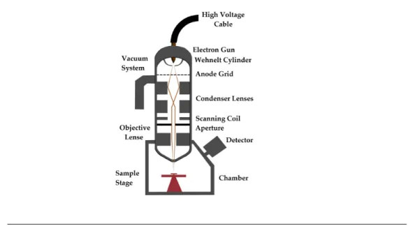
The interior parts of the SEM are shown In figure 2.1. Although the parts can be different
for various types of SEM’s, the basic principles are the same. The electron beam is created at
the electron gun, which can be for examle a hot filament made from Tungsten or Lanthanum
Chapter 2. Experimental Methods 11
Figure 2.1: Schematic design of the SEM interior
thermal emission, i.e. the energy barrier of the work function is crossed. This same principle
has been used for many years in CRT televisions. The Fei Nova Nanosem, however, makes
use of a different type of electron gun, namely a Schottky field effect emitter. This is a
very sharp emission source and can achieve much higher signal to noise ratio in SEMs [15]. In the presence of a large electric field, the pointy shape of this emitter enhances the local
field, which will lower the work function of the material. The low work function enables the
electrons to be emitted much easier. This makes high current densities possible. The emitter
of field emission electron guns can be Tungsten or Tungsten coated with a low work function
material such as ZrO2. The free electrons from the electron gun are attracted to the anode
by a very high positive potential (for the EBPG the maximum anode potential was 30 kV).
To create a highly directional electron beam, the diagonal elements are blocked by a Wehnelt
cylinder and a uniform beam comes out. The complete interior of the SEM is in an ultra
high vacuum, because the electrons are not allowed to collide with gas molecules. In the Fei
Nova Nanosem, the vacuum was near 10−5 mbar for the lower chamber up to 10−10 mbar near the electron gun. The beam spot size on the sample, related to the FWHM of the beam,
is controlled by the pair of condenser lenses. After the condenser lenses, the beam travels
through an aperture, which can be set to different diameters. The aperture size changes the
amount of current in the beam that will illuminate the sample. Finally, the beam travels
through another lens pair, which is used to focus the beam onto the sample. Interactions
of the electrons with the sample, can have several consequences, namely electrons can be
backscattered or secondary electrons can be emitted by the material. Both types of electrons
are collected by a detector and the intensity is measured. The beam can be moved by the
scanning coils to scan each point on the sample. Each point on the sample will correspond
Chapter 2. Experimental Methods 12
measured on that particular spot on the sample.
2.1.2 From SEM to EBPG
The EBPG has the same capabilities as the basic SEM, apart from the possible improvements
to obtain better images. With the EBPG images can be created of the sample and the beam
can be scanned across the sample in all types of patterns. The latter is the most important
property. To write small nanostructures with the electron beam, it is necessary to add a
small polymer resist layer on the substrate. The most used resist layer is PMMA, which
can have different polymer chain lengths, discovered in 1968 [16]. The PMMA type used, was PMMA with an average molecular weight of 950kDa (9,5.105 atomic units in weight). When this layer is irradiated by electrons ,two things can happen. At low doses the polymer
chains are broken by the electrons. In this case it is called a positive resist. However, at
higher doses, the polymerization becomes enhanced and larger chains are formed. In this
case, it is called a negative resist. With PMMA, structures of very high resolution can be
obtained, but this can differ for each type and even layer thickness. For PMMA as a positive
resist, 3 nm linewidths of NiCr wires with 100 nanometers seperation between the wires have
been achieved [17]. For negative tone resists, only 15 nm linewidths with 30 nm seperation between the wires has been achieved. The required dose for the latter case was even 100
times higher [18]. The difference in obtained linewidths may be attributed to the proximity effect, which is introduced later in this chapter.
The parts that had to be exposed by electrons on the resist were pre-designed in the e line
software. As a substrate, p-type Boron doped Silicon with a thermal oxide layer of 300
nm was used initially. To apply the PMMA resist, a droplet of PMMA 950kDa 3 percent
in weight in Anisole was pipetted on the substrate and spincoated at 4000 rpm to make a
uniform layer. Subsequently, the layer was baked for two minutes at 180 oC to remove the remaining solvent. The thickness of the PMMA layer was now around 250 nm. The sample
was placed inside the sample holder of the EBPG chamber and with a diamond pencil a
small scratch was made in the left down corner. This was done to retrieve this position with
the electron beam imaging system. The chamber was pumped down to a vacuum of around
10−4 mbar. At this pressure imaging of the sample is possible, but the sample should not be exposed too long to the electron beam, because the beam causes depolymerization of
the resist. Before imaging, one of the 32 predefined beam currents has to be chosen. The
smallest structures should be written with a low beam current, because then the spot size
is small as well. However, for very large structures, a high beam current is necessary to
reduce the write time. The size range can be very large, as 1mmx1mm structures compared
Chapter 2. Experimental Methods 13
corner of the sample will be assigned to be the center of a two dimensional axis system. The
structure will be written in this coordinate system. But first, the sample stage has to be
aligned in the coordinate system. This procedure is done by imaging a particle, with a size
of less than 1 µm, at a high magnification of 105x. The stage moves a larger distance and then attempts to retrieve the initial position. Any deviation between the intial and final
positions will be corrected for. Through this correction, a stage movement precision of 2 nm
can be achieved. A stage movement is only necessary when the structure is larger than the
writefield of 100x100 µm2. Then the stage will move automatically to the next writefield, when the previous writefield has been exposed. The writefield itself is exposed by moving
the electron beam with the scanning coil. The exposure is done automatically by computer
numerical control. A certain base dose is required for the structures to be written. To find
this base dose, it is best to do some test writings, before writing the actual structures. During
this test, multiple doses are used for the same structure and the dosage that gives the most
appealing structures is used for the whole structure.
Figure 2.2: The process of electron beam lithography depicted schematically in steps.
After exposure, the depolymerized parts are still present on the sample. These parts, will be
removed by a selective solvent, which is called a developer. In this developer, the
depolymer-ized parts will dissolve much faster than the non-exposed parts. The better the difference
between this solubility, the better is the resolution of this resist. The procedure used, was
to submerge the resist layer for 40 seconds in a mixture of MIBK:IPA 1:3 and afterwards
submerge for 30 seconds in IPA alone. The first solvent will initiate the development, while
the latter will stop it. Then the sample is rinsed with more IPA and blow dried with N2.
The structures can be checked with an optical microscope, if they are large enough. The
whole process is schematically depicted in figure 2.2.
After development, the sample can be coated with a thin metal layer. This layer should be
smaller than the thickness of the resist, to make it possible to remove the resist afterwards.
The metal layer can be evaporated onto the sample in the resistance evaporator. A schematic
of the evaporator is shown in figure 2.3. The sample is first loaded upside down in the
loadlock, which is seperated from the lower chamber by a valve. Then the loadlock is pumped
seperately from the chamber by a turbo pump, down to a pressure of 10−6 mbar, before the valve is opened. Subsequently, the sample holder is lowered into the chamber and the whole
Chapter 2. Experimental Methods 14
Figure 2.3: Schematic of the resistance evaporator for thin film growth.
required to grow layers with as least impurities as possible. In the schematic, only an Au
boat is shown, but there are two other metals available, which can be selected by a switch. As
an adhesion layer to the substrate, Cr is required. This one is selected first and the voltage
is driven up and a high current will flow through the boat. Due to the resistance of the boat,
the wire will heat up by Joule heating. At a certain voltage, the heating is large enough to
evaporate the chromium in the chamber. The chromium gas will hit the sample and forms
a thin layer on it. The thickness and growth rate is monitored by measuring a crystal’s
resonance frequency which is related to the thickness of the grown layer. A minimum rate of
0.1 ˚A/s is measurable. Only a few nm of the adhesion layer is necessary. Then an Au layer
can be evaporated onto the sample with the same process. After unloading, the sample is
submerged for a few hours in acetone. The acetone dissolves the excess PMMA, which is still
on the positions that were not exposed by the electron beam. The PMMA dissolves better
when the Acetone is heated to 40 oC. Instead of evaporation, sputtering was also done to
grow a thin layer. In the sputtering machine, the adhesion layer was MoGe with a top layer
of Au. When the Au is difficult to remove outside the structures, some flow was created with
a pipette. If this would not work, then the sample was sonicated, but care must be taken to
not destroy the structures.
2.1.3 Proximity effect
At this point, the structures are ready, but there are still many things to improve. Because
the structures are very small, some effects can already have a large impact. An example of
such an important effect is the proximity effect. The proximity effect is the depolymerization
Chapter 2. Experimental Methods 15
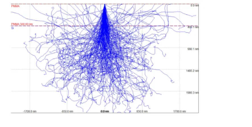
nuclei in the resist or substrate and by the secondary electrons. Monte Carlo simulations
have revealed that many electrons can penetrate into the surroundings of the structures. The
results of the trajectories are shown in figure 2.4.
Figure 2.4: This Monte Carlo Simulation shows the trajectories of 200 electrons from a 15 keV electron beam in a PMMA layer of 500 nm thick. The electrons are generally bended into the surroudings of the spot and can even move upwards, out of the substrate. The Guassian shape of the electron beam spot is broadened by the proximity effect. The image
is obtained from [19].
The proximity effect is dependent on the acceleration voltage. It reduces when the
accelera-tion voltage is increased, because the electrons will peneratre deeper into the substrate and
interact less with the resist. For very low accerelation voltages, the effect will be huge [19]. The raith EBPG can produce electrons with energies from 100 eV up to 30 keV. The voltage
was always kept at 30 kV to minimize the proximity effect. There are complex formulas
available to correct for the proximity effect [20]. These were not used in the structures, because a complex treatment was not necessary to achieve good results. The only correction
made, was that larger structures in the vicinity of nanostructures, received less dose than
the nanostructures.
2.2
Fabricating Single Electron Devices
As a starting point of creating single electron charging devices, electrodes are fabricated.
These electrodes are created by electron beam lithography. However, the particle cannot be
defined by electron beam lithography, because the size is beyond the limits of this method.
How to obtain the island with tunnel junctions will be discussed later.
2.2.1 Electrodes with Nanometer Seperation
To fit a very small particle between the electrodes, the electrode seperation has to be very
Chapter 2. Experimental Methods 16
in one of the lucky cases a few tenths of nanometers. There are ingeneous ways to make a
seperation of just a few nanometers. One of these methods is called the shadow evaporation
method, where the electrodes are designed with a small overlap. Initially, one of the electrodes
is written and metal is evaporated. Then, again the sample is covered with PMMA and the
second electrode is written. However, this time evaporation is done at an angle. The shadow
of the first electrode makes sure that there is a small spot that will not be covered. The
angle and height of the second evaporated layer will then determine the size of the gap. The
final gap sizes were reproducibly made between 3 and 10 nm [21]. This would be precisely in the range to fit a very tiny particle. A second method is the production of nanogaps by
means of electromigration.
2.2.2 Electromigration
Electromigration is the formation of voids and eventually electrical breakdown at high
cur-rent densities in conducting wires. The breakdown is caused by momentum transfer of the
conduction electrons to the ions, leading to a drift of the ions [22]. To form the nanogap, the limit of electrical breakdown has to be reached. In many cases this would be very rapid
and the actual size of the gap formed, will not be controllable. To gain control on the final
gap size, an active feedback system has to be used [23]. This feedback system continuously samples the current at an applied voltage and calculates the resistance. If the resistance has
not increased significantly by x percentage, then the voltage is increased by a small step.
However, if the resistance has increased more than x percentage, the voltage is set back to a
safe value. This process is repeated every cycle, until the desired resistance value is reached.
An example of an IV curve, produced by this feedback mechanism, is shown in figure 2.5.
The resistance value of the gap can be related to the gap size by fitting the IV curve with
the Simmons model [24].
A similar feedback system was used in this project. The voltage applied would start at a safe
value of 100 mV and then will be ramped up in steps of 10 mV. The schematics of the setup
used is shown in figure 2.6. The applied voltage generates a current, which is converted into
a voltage by the IV convertor on the left. The voltage range of the IV convertor is from -10 V
to 10 V. The IV convertors’ resistor, RA, defines the amplification of the current into voltage.
This amplification must be chosen carefully to have the best resolution i.e. the highest output
voltage per ampere, but still in the given range. In general, an amplification of 103 V/A was used. The total resistance of the device is then calculated by dividing the voltage through
the measured current. However, this is the total resistance of the whole circuit and includes
the resistance of the microprobes. These microprobes are Tungsten needles with a 7µm tip,
touching the rectangular contacts on the sample. The contact resistance of the probes can
Chapter 2. Experimental Methods 17
Figure 2.5: In this IV plot the evolution of the electromigration is shown. The IV curve starts linearly up to 0.8V. At this points, it bends downwards. Therefore, the resistance starts to increase rapidly. At the end of the curve, the resistance hits a threshold and the voltage is set back to a safe value. The arrow indicates the direction of the sequence of
measurements. This figure was obtained from [23]
to do a 4 probe measurement. These probes are positioned between the source and drain
contact. The voltage drop measured between these two added probes, divided through the
measured current, yields approximately the resistance of the nanoconstriction.
Figure 2.6: The schematical setup for the electromigration experiment is shown here. The
output voltage is controlled by the feedback system, where the feedback is based on the voltage input of the IV convertor on the left. The feedback system makes sure that the
tunnel junction formed in the wire has a predefined size.
As depicted in figure 2.6, there is a constriction in the wire. This constriction is necessary
to define the location where the electromigration has to occur. Because the resistance is
highest in the constriction, Joule heating will initiate here. This Joule heating must not
dominate over the electromigration. Therefore, the wires connecting the constriction must
have a low resistance compared to the resistance of the constriction. Then, the heat formed
in the constriction by Joule heating can be efficiently conducted to the large reservoirs. The
Chapter 2. Experimental Methods 18
p(t) =pc
h1 +Rs/Rc(0)
1 +Rs/Rc(t)
i2
(2.3)
To reduce the resistance of the leads, the structures can be designed in a bow-tie form [25]. The researchers of [25] also evaporated a thicker gold layer in the leads than in the small restriction. This made the difference between the lead resistance and constriction resistance
larger. Successively, the finished nanogap can accomodate an island. A good source for the
island is the gold nanoparticle.
2.3
The Nanoparticle Island
Gold nanoparticles exist in many sizes. The sizes used were on average 5 nm up till 100
nm. All particles were produced by the reduction of HAuCl4 and sodium citrate in millipore
water. This is the so-called Turkevitch method, named after its discoverer [26]. Particles of 10 nm were produced by ourselves. The other sizes were from a commercial source. The
size of the particle is important for the resulting charging energy. A 10 nm spherical particle
would have a theoretical self-capacitance of 1.1 aF. Therefore, the charging energy will be
73 meV. 2 nm particles are also available commercially, but they have a high dispersion. A
2 nm nanoparticle would have a charging energy of 365 meV.
Small gold particles can also be produced by evaporating directly onto the sample with the
electrodes. In the early stages of evaporation, the gold doesn’t form a thin film directly,
but gold starts to accumulate on particular spots. These small Au grains can have sizes of
as small as 5-15 nm, when only 2 nm of Au is evaporated. A Coulomb blockade has been
observed in these type of structures [27].
An ingeneous method to trap the gold nanoparticles in the nanogap is called
’dielectrophore-sis’.
2.3.1 Dielectrophoretic Trapping of Nanoparticles
The setup for trapping nanoparticles in the nanogap is shown in figure 2.7. An AC voltage is
created by a frequency generator on the right. The frequency of the voltage signal is typically
in the range of 100 KHz to 1 MHz. The signal then travels through a capacitor of 6.8 nF,
which blocks any DC components in the signal. This is done to avoid electromigration, which
could increase the size of the gap. A high alternating electric field will be created between
the electrodes. Initially, the voltage drop across the gap is almost equal to the input voltage,
Chapter 2. Experimental Methods 19
Figure 2.7: A schematic of the setup for trapping nanoparticles between electrodes. On the right electrode, an AC voltage is produced, which creates a high alternating electric field in the nanogap. The surrounding medium is the water droplet, with nanoparticles suspended. The particles will be attracted to the gap and ultimately they will create a bridge across the two electrodes. The status of the trapping experiment can be observed on the screen of the
oscilloscope.
in series. The voltage drop across this resistor was monitored by the oscilloscope. Directly
above the gap, a small droplet of gold nanoparticles suspended in water is pipetted. Due to
the high AC electric field, the gold nanoparticles are polarized in the same direction. But
the field is not homogeneous on both sides of the nanoparticle. Therefore, the particles are
attracted to the point where the field is highest, namely between the electrodes. Eventually,
the nanoparticles will bridge the gap. The nanoparticle bridge will reduce the voltage across
the gap, until the voltage across the resistor becomes substantial. This, in general, rapid
event can be observed on the oscilloscope. Whole wires of nanoparticles can be formed with
this method [28].
The requirements for a particle to show a behaviour as described above, can be best explained
by an equation. Accordingly, the dielectrophoretic force on a nanoparticle can be expressed
as follows:
< ~FDEP >=πmr3
h(p−m)
p+ 2m
i
∇|E2| (2.4)
Evidently, the force scales with the size of the particle: r3. Because the drag force of the fluid only scales with r, the larger particles will have a larger net force. More important is
the term between brackets, which is called the Clausius-Mosotti factor. It determines the
sign of the force on the particle and the magnitude. The termm is the dielectric constant
of the medium and p is the dielectric constant of the particle. When m is larger than p,
the particles are attracted to the positions between the electrodes. This is called positive
Chapter 2. Experimental Methods 20
attracted to positions of low field intensity i.e. they will be repulsed from the gap. However,
there is a way to trap particles with negative dielectrophoresis by designing a four electrode
structure, called a quadrupole trap. In the middle of this trap the field has a minimum. With
negative dielectrophoresis, single beads of as small as 7.5µm have been trapped successfully
[29]. Negative dielectrophoresis is not possible for gold nanoparticles, because the relative dielectric constant at frequencies in the range of a frequency generator is approximately 1.
Only at optical frequencies, the dielectric constant becomes complex and would take different
values [30]. The relative dielectric constant of the water medium is 78.2 at room temperature. This huge difference in dielectric constant, for water and the gold nanoparticles, makes the
dielectrophoretic force very large.
Instead of gold nanoparticles, also CdSe quantum dots have been used, with a 655 nm
fluorescence peak. The quantum dots have a size dependent relative dielectric constant,
but it is around 6.2 [31]. Therefore, depending on the fluid medium, it is possible to trap them both with a positive or negative dielectrophoretic force. In the gap, the fluorescence
properties can be studied under high electric fields.
2.3.2 Coating the Gold Nanoparticles
By the bridging of the nanoparticles in the gap, a low-ohmic connection is formed. This
is not desired for single electron charging experiments. By coating the surface of the gold
nanoparticle with a large non-conducting molecule, a natural tunneling barrier between the
electrode and the gold nanoparticle can be constructed. The natural tunneling barrier can be
a thiol molecule. For example, octanethiol or an even larger molecule such as dodecanethiol.
The latter was used as a coating in this project. To apply the dodecanethiol coating, the
solution first has to be centrifuged for an hour at 15000 rpm and 100C. The rotating motion will force the particles to sink to the bottom of the 1 ml eppendorf tube. Afterwards, the top
layer of water can be pipetted out of the eppendorf tube. Then, 1 ml of ethanol is added to the
particles and they are redispersed by sonication. Inside a glovebox, the dodecanethiol is added
to an ethanol solution, which is saturated with N2 to avoid oxidation of the dodecanethiol.
Both solutions of the ligand in ethanol and the ethanol with nanoparticles are combined
and the coating process of the nanoparticles initiates. After the solution has spend a few
days in a fridge, the coated particles will have sunk to the bottom and the ethanol can be
pipetted out again. Finally, any solvent of choice can be added to the coated particles. But
nonetheless, it is preferred that the solvent dissolves the thiol molecule. For example, the
alkanethiol molecules are not soluble in water. To observe dielectrophoresis of the particles, a
non-volatile solvent has to be used. Before, a toxic mixture of 1:1 Hexane/Dichloromethane
Chapter 2. Experimental Methods 21
Figure 2.8: Artist impression of electrodes with a Au nanoparticle coated with the water soluble molecule dithiothreitol.
Thiol molecules can also be made water soluble by adding hydroxide groups. For example, the
molecule dithiothreitol. This molecule contains two hydroxide groups, but has a short length.
Therefore, the tunneling barrier will be small and is actually in the range of a few Mohms.
Yet, Coulomb blockade had been measured in devices, which contained dithiothreitol coated
nanoparticles between electrodes [32].
2.4
Optical Experiments
The substrate of the device can be of any material. However, the optical experiment requires
that the substrate is transparent, such as glass. Unfortunately, the downside of glass, is that
it is electrically insulating. Therefore, the electrons can charge the sample during EBL and
this accumulation of charge will distort the pattern by repulsing the beam [33]. Fortunately, there are ways to overcome this charging effect. It requires a small, but not so easy, change
in the process of EBL. All other methods, described before, remain possible.
2.4.1 Electron Beam Lithography on a Glass Substrate
There are different ways to produce patterns on insulating substrates. The most used method
involves PEDOT:PSS. This is an organic polymer, which is soluble in water and can be
spincoated on top of PMMA. The PMMA is not water soluble and therefore will not be
affected. The nanolayer of PEDOT:PSS will dissipate the trapped charges during EBL. It
will also block some charges of the electron beam from arriving at the PMMA. Hence, a
higher electron dosage will be necessary for the structures. Finally, when the patterns have
been written, the layer can be removed easily with water and the PMMA can be developed
as before [34].
Another method that was used in this project involved the evaporation of a layer of a few
nm Cr on a glass slide and then spin coating a PMMA layer on top of it. Subsequently, the
Chapter 2. Experimental Methods 22
Figure 2.9: Steps in fabrication of structures on a glass substrate.
the lift off. Lastly, the Cr layer had to be removed again. This can be done by either wet
etching methods or dry etching methods. Examples of wet etchants of chromium are hydrogen
peroxide, hydrochloric acid or hydrofluoric acid. Due to passivation of the chromium layer,
it may well be that the surface first has to be reduced electrically, before etching takes place
[35]. A dry etching method of Cr can be done by a plasma, which is the reaction of ionic gases with the Cr. The used plasma gases can be chosen such that the etching rate for the
Cr will not be lower than the etching rate for Au. The Au on the structures must remain,
once the Cr is gone. Another dry etching method is ion beam etching, which is the uniform
bombardement of the sample with ions, knocking away material. The followed procedure of
sample preparation on glass, including dry etching, is depicted in figure 2.9.
2.4.2 Fluorescence Microscope
Figure 2.10: Schematic impression of the optical setup of the fluorescence microscope.
The optical beams, going through the setup, are depicted as well.
For example, to study the properties of quantum dots, a microscope setup is necessary
to excite the quantum dots and simultaneously observe the fluorescence. Such a setup is
Chapter 2. Experimental Methods 23
than the absorption energy of a quantum dot. The laser light will be guided through a system
of mirrors and a wide angle lens. Of which the latter makes sure a larger part of the sample is
illuminated. Before the light hits the sample, it has to travel through an objective lens, which
focuses the light. The fluorescent and reflected light travel backwards and then through the
beam splitter. After another mirror, the light hits an optical filter. This filter blocks the
light of the laser and only transmits the light from the fluorescence. The fluorescent light is
collected by the CCD camera and images the quantum dots or any other fluorescent object.
If there is a gap structure on the glass slide, a droplet of these quantum dots in water can
be pipetted on the gap. When the laser is focused to the gap, the movement of the quantum
dots could be tracked, by observing the fluorescent light on the camera. When an AC voltage
is applied to the gap structure, it could be that there is a collective movement of the particles
to the gap observed, due to the positive dielectrophoretic force.
The same setup is necessary when observing the fluorescent light of single molecule probes.
However, to observe zero phonon lines, the sample has to be cooled down to low temperatures
in a cryostat. A window in the cryostat will make sure the light will hit the sample. Again a
part of the fluorescent light and reflected light will be collected and filtered. With a camera
the source of the fluorescence will appear as a spot, in analogy to the spot of a quantum dots’
fluorescence. With the Gaussian shape of the intensity of the spot, the particle positioned
can be determined very accurately, by fitting it to a point spread function. This method can
Chapter 3
Experimental Results
3.1
Building Single Electron Devices
The first requirement for creating a SET or a single electron box, is a set of electrodes with
enough space in between to fit a nanoparticle, with the nanoparticle surrounded by tunnel
junctions. Different methods to create these electrodes with a small spacing are possible,
but it’s generally a matter of trial and error to find the method producing the best results.
A subset of these methods, that were undertaken in the fabrication steps of this project, are
outlined in the coming sections. All of these practices had their own benefits and were useful
for different types of experiments. As a starting point all the fabrication of devices required
the use of electron beam lithography (EBL), which was explained into detail in section 2.1.
Therefore, the results of EBL are discussed first.
3.1.1 Creating Nano-Electrodes
Firstly, the structures were designed in the e Line software. They were designed to have as
much overlap as possible in the wiring connecting the nanostructures, because a different
beam current is necessary to write these parts. When switching to a different beam, the
beam can displace up to 10 µm. Therefore, the overlap will avoid that the structures are
disconnected. However, this should not be done very close to the nanostructures itself, to
avoid failure caused by the proximity effect. The best solution was an overlap in the order of
10µm in both the x and the y direction. Instead of using such a big overlap, it is also possible
to develop the small structures and perhaps markers after they have been written. Preferably
markers are used, because then the structures will remain preserved. An alignment on the
markers or parts of the structures can be done to retrieve the positions on the wafer. This
Chapter 3. Experimental Results 25
realigning procedure will achieve a very high precision in the final structures, but takes more
time.
On the Si/SiOx waferpieces, the required dose for the structures with electrodes seperated
by a nanogap, was approximately 260µC/cm2 for the PMMA 950 kDa resist. This dose was used in general for all the structures in the course of the project, whenever no initial dose
test was performed. The first design consisted of two overlapping arrow shaped electrodes.
The overlap was programmed to be 30 nm and constituted a sort of thin constriction in the
wire. The results of two of these wires, imaged with an SEM, are shown in figure 3.1.
Figure 3.1: Both wires were designed the same and created with EBL. SEM inspection
shows they are very different. The wire above has a gap of close to 40 nm in width and the bottom wire has a constriction of approximately 30 nm wide. Therefore, the bottom wire is
in most agreement with the original design.
Although the wires were designed to have a 30 nm overlap, the outcomes are completely
different. The electrode on the bottom conforms best to it’s design. The upper one contains
a relatively large gap. However, both electrode structures can be used in a sequence of steps
to create single electron charging devices. A list of the possible sequences applicable to the
devices in figure 3.1, which were all undertaken, is shown below:
• A nanoparticle can be trapped directly into the large gap by dielectrophoresis
• The constriction can be electromigrated to form a gap and a particle can be trapped
into this gap with dielectrophoresis
• Dielectrophoresis can be used to create a nanowire in the gap. This nanowire can be
electromigrated again to create a smaller gap and a single particle can be trapped inside
again by dielectrophoresis.
Chapter 3. Experimental Results 26
3.1.2 Nanoparticle Trapping in an EBL defined gap
As the chargeable island of a single electron device, gold nanoparticles were used. They
can be very easily obtained commercially or by synthesis. Both sources have been used.
Although, for the synthesis only particles of 10 nm with low dispersion were obtained. For
the commercial nanoparticles were different sizes obtainable. The average sizes varied from
5 nm up to 100 nm. Yet to obtain Coulomb blockade at reasonable temperatures, the
rule is: ’the smaller, the better’. The gold nanoparticles were ’dissolved’ in water in very
high concentrations of 1010-1014particles/ml. For smaller particles, the concentration is the highest, whenever the source uses the same amount of reactant. The solutions show a deep
red color for 5 nm particles, up to orangish for 100 nm particles. The initial concentration
of particles is way too high for dielectrophoretic trapping of single particles. If the solution
was not diluted, large clusters of particles would be trapped between the electrodes in the
blink of an eye. The dilution was around 10-100 times, depending on the average sizes. 5
nm particles would be diluted for 100 times and 100 nm particles for 10 times.
The schematical setup of the dielectrophoresis experiment was already shown in the figure
2.7 of the previous chapter. A 6.8nF capacitor was used in the circuit to block the DC
current and a 1 Gohm resistor was placed in series. The voltage drop across the resistor was
compared to the input voltage with an oscilloscope. Initially, the immensly wide gap has a
much larger resistance than the resistor. Therefore, the voltage drop would be entirely over
the gap. Thus, the voltage measured on the resistor is close to 0. A droplet of the diluted
solution of gold nanoparticles was pipetted onto the junction. The wires connecting the
electrode to a contact pad were designed to be sufficiently large, to not let the microprobe
touch the droplet. The sharp tip of the microprobe would create large electric fields as well,
which would cause the nanoparticles to move to it. The amount of liquid in the droplet was
in the range of 20-50 µL. When the droplet was in the right place the voltage was applied
with a function generator. Only 1-2 V was necessary, at a frequency range of 1kHz - 1
MHz, to bridge the gap with particles in a few seconds. Eventually, the trapping event was
confirmed by the increased voltage across the resistor, measured on the oscilloscope. Once
the connection was made, the voltage could be ramped up for a few seconds (up to 4 V) to
melt the particles and form a wire connection. An example of this is shown in figure 3.2,
where a molten wire of the nanoparticles is depicted with a SEM.
A wire, such as in figure 3.2, can be electromigrated to create a much smaller gap. This has
been done succesfully in different samples. Instead of capturing many particles to create a
bridge, a single particle can also be trapped directly. Then, the gap has to be small enough
to fit a single particle. Again, the same procedure is followed as before. But this time, there
is not a clear signal when a single particle has been trapped and contains two large tunnel
Chapter 3. Experimental Results 27
Figure 3.2: Dielectrophoretic trapping of 10 nm nanoparticles created a bridge across the
two electrodes. Subsequently, a high AC voltage of 6V was applied for a few seconds to melt the particles and form a nanowire.
high. The voltage drop of 1 Gohm tunnel junctions in the gap would then still be measurable
with the oscilloscope. For nanoparticles, which were not coated with a ligand, there were
some successfull trapping events of a few particles. A particular case, where three particles
were trapped between the electrodes, is shown in figure 3.3. From the SEM image it cannot
be concluded if there is an Ohmic contact between one of the sides of the particle with the
electrode. The IV curve, shown on the right of figure 3.3, does show a resistance in the
regime of tunneling. The uncoated particles of 10 nm have a theoretical charging energy
of 73 meV, which is larger than the thermal energy at room temperature. Therefore, even
at room temperature some Coulomb blockade should be visible. This is not evident from
the figure. There might be on one side of the particle a contact with the electrode. It was
undertaken to measure an IV, with the sample submerged in liquid nitrogen. Unfortunately,
no electrical contact was measured.
To ensure there is a tunnel barrier between the electrode and particle, the particle can be
coated with a ligand. The length of the ligand will be the width of the tunnel barrier.
The coating process is described in section 2.3.2. An octanethiol coating (C8) for 10 nm
nanoparticles required a concentration of 0,14 mol/L coating. The coating solution with
nanoparticles was sonicated to enhance the exchange. Storing the solution for a few days
in a fridge would precipitate the coated particles. Then, the solvent can be removed with
a pipette and any solvent of choice was added. For dielectrophoresis, the type of solvent
matters, for the following reasons:
• The dielectric constant of the solvent should be large to increase the dielectrophoretic
force
Chapter 3. Experimental Results 28
Figure 3.3: (a) Between the electrodes three visible individual nanoparticles were trapped. (b) In the middle is shown the IV curve for this junction at room temperature. The resis-tance, obtained from the curve, shows that there is tunneling. However, it is not clear if this tunneling behaviour is on both sides. (c) Probes in contact with the sample, submerged in
liquid nitrogen, to perform low temperature IV measurements.
• To be able to form a droplet, the solvent should be polar
The latter was actually difficult to implement, because the alkanethiol ligand only dissolves
well in apolar solvents and only slightly in more polar solvents. Different solvents were
sampled on their properties, but the results were not positive. There was no observed positive
dielectrophoresis for any solvent. Because bare gold nanoparticles have a relative dielectric
constant of nearly 1 in the used frequency range, it should show for almost every solvent a
positive dielectrophoresis. For Toluene, with it’s relative dielectric constant of 2.38, there
should be positive dielectrophoresis. But even for toluene, there was no particle trapping
observed. Toluene was chosen for it’s high boiling point, but it is non-polar and therefore
doesn’t form a firm droplet. The solution was therefore also in contact with the probes and
it was observed that after dielectrophoresis, the probes were covered with the particles.
3.1.3 Gap Creation by Electromigration
Gaps created by EBL are generally very large and the sizes of the gaps always deviate
strongly from the design. A method, which was used to get a lot more control on the
final gap size, is feedback controlled electromigration. This method is generally used to
create gaps of a smaller size, than the size of the smallest nanoparticles that were available
(average of 5 nm). Therefore, the feedback doesn’t have to respond very fast. With labview
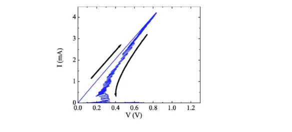
a program was written to controllably electromigrate a nanowire. Figure 3.4 shows an IV
curve of a succesfull controlled electromigration. The chronology of the process is from the
upper curve of the first cycle to the bottom curve for the last cycle. A cycle begins at the
assumed safe value of 100mV and then the voltage is incremented in small steps. For the
Chapter 3. Experimental Results 29
have enough momentum to dislocate the atoms in the constriction and effectively narrow
the constriction. When the resistance had hit a value of around 1 Mohm the process was
terminated. Eventually, in the case of figure 3.4, the remaining tunneling resistance of the
created gap was a few megaohms. This indicated that the feedback loop had done its job
quite well.
Figure 3.4: The upper curve is the first cycle in the electromigration process. From top to
bottom the curves are chronologically shown for all cycle steps. The wire before and after electromigration dont look exactly the same, because the magnification factor is different
and there is some deflection of the electron beam during imaging.
Not in every case is the feedback loop successful in creating a gap with full control.
Some-times, the Joule heating can be substantial, leading, as discussed in section 2.2.2, to rapid
breakdown of the wire. Such an event is observed in figure 3.5, where the resistance suddenly
jumps to a large value. This jump will terminate the feedback loop and turn the voltage to
a safe value of zero. The final resistance was still measured to be 144 Gigaohms.
Figure 3.5: On the left is shown the IV curve of the electromigration process. The first
cycle is terminated rapidly and then the process is finished i.e. the gap formation process was not controlled.
3.1.4 Parallel Electrodes
Fabricating structures of two electrodes with a single junction gives a lot of variety in the
Chapter 3. Experimental Results 30
from somehow. Yet to have single electron charging on a time scale accessible to single
molecule optics, the charging time needs to be large enough (see section 1.0.5). Therefore, to
increase the probability of ending up after dielectrophoresis with a junction exhibiting single
electron charging on these accessible timescales, parallel electrodes were created. A total of
50 junctions were designed parallel, with a distance of 2µm in between. All these junctions
were connected to the same electrode pair, with a 1,5 mm long wire leading to the contact
pads.
Figure 3.6: (a) Shows the parallel electrodes connected on one side to the same electrode.
(b) Formation of a wire of 100 nm gold nanoparticles by dielectrophoresis. (c) Next to the right electrode is a nanoparticle. The configuration resembles a sort of single electron box.
The large electrode and tunnel barrier could make the discharge time large enough.
In figure 3.6, the result after dielectrophoresis with 100 nm paritcles, is shown in the two
right images. In one case a bridge has formed across the electrode pair and in the right image
a particle is in closest contact with the right electrode. The right electrode might be used to
charge the particle.
Unfortunately, the cryostat was down and single molecule optics was not possible in the
course of months. At this point, fabrication was only done on Si/SiOx, as a substrate. The
substrate might reflect a lot of light in optical experiments. Therefore glass would be a better
choice. Additionally, it is for most experiments better to shine the light through the sample.
An experiment with quantum dots, proposed in section 1.4, would then also be possible.
Though, fabricatiog on glass would still be a new challenge. Therefore, the possibilities had
to be examined. These are outlined in the next section.
3.2
Electron Beam Lithograhy on Glass as a Substrate
Glass is an insulating substrate. Hence, exposure to the electron beam will charge the
substrate and deform the pattern. The accumulating charges can be dissipated by adding a

![Figure 1.3: Experimental result of an IV characteristic of a SET [ 7]. The Coulomb blockade survives up to a voltage of 12,2 mV](https://thumb-us.123doks.com/thumbv2/123dok_us/8213487.2177557/10.893.174.684.223.483/figure-experimental-result-characteristic-coulomb-blockade-survives-voltage.webp)