MOTOROLA.COM/SEMICONDUCTORS
HCS12
Microcontrollers
S12CPUV2/D Rev. 0
S12CPUV2
Reference Manual
Motorola and the Stylized M Logo are registered trademarks of Motorola, Inc. DigitalDNA is a trademark of Motorola, Inc.
This product incorporates SuperFlash® technology licensed from SST. © Motorola, Inc., 2003
S12CPUV2
Reference Manual
To provide the most up-to-date information, the revision of our documents on the World Wide Web will be the most current. Your printed copy may be an earlier revision. To verify you have the latest information available, refer to:
http://motorola.com/semiconductors
The following revision history table summarizes changes contained in this
Revision History
Reference Manual S12CPUV2
4 Revision History MOTOROLA
Revision History
Date Revision
Level Description
Page Number(s)
July,
Reference Manual — S12CPUV2
List of Sections
Revision History 4 List of Sections 5 Table of Contents 7 List of Figures 15 List of Tables 17
Section 1. Introduction . . . 19
Section 2. Overview . . . 25
Section 3. Addressing Modes . . . 33
Section 4. Instruction Queue . . . 51
Section 5. Instruction Set Overview . . . 59
Section 6. Instruction Glossary . . . 91
Section 7. Exception Processing. . . 315
Section 8. Instruction Queue . . . 327
Section 9. Fuzzy Logic Support . . . 341
Appendix A. Instruction Reference . . . 381
Appendix B. M68HC11 to CPU12 Upgrade Path. . . 409
Reference Manual S12CPUV2
6 List of Sections MOTOROLA
Reference Manual — S12CPUV2
Table of Contents
Revision History 4 List of Sections 5 Table of Contents 7 List of Figures 15 List of Tables 17
Section 1. Introduction
1.1 Introduction . . . .19
1.2 Features . . . .19
1.3 Symbols and Notation. . . .20
1.3.1 Abbreviations for System Resources . . . .20
1.3.2 Memory and Addressing . . . .21
1.3.3 Operators . . . .22
1.3.4 Definitions. . . .23
Section 2. Overview
2.1 Introduction . . . .252.2 Programming Model . . . .25
2.2.1 Accumulators . . . .26
2.2.2 Index Registers . . . .26
2.2.3 Stack Pointer . . . .26
2.2.4 Program Counter . . . .27
2.2.5 Condition Code Register . . . .27
2.2.5.1 S Control Bit . . . .28
2.2.5.2 X Mask Bit . . . .29
2.2.5.3 H Status Bit. . . .29
2.2.5.4 I Mask Bit . . . .30
2.2.5.5 N Status Bit. . . .30
2.2.5.6 Z Status Bit . . . .30
Reference Manual S12CPUV2
8 Table of Contents MOTOROLA
Table of Contents
2.2.5.8 C Status Bit. . . .31
2.3 Data Types . . . .31
2.4 Memory Organization . . . .32
2.5 Instruction Queue . . . .32
Section 3. Addressing Modes
3.1 Introduction . . . .333.2 Mode Summary . . . .33
3.3 Effective Address . . . .33
3.4 Inherent Addressing Mode . . . .35
3.5 Immediate Addressing Mode . . . .35
3.6 Direct Addressing Mode . . . .36
3.7 Extended Addressing Mode . . . .37
3.8 Relative Addressing Mode . . . .37
3.9 Indexed Addressing Modes . . . .38
3.9.1 5-Bit Constant Offset Indexed Addressing . . . .41
3.9.2 9-Bit Constant Offset Indexed Addressing . . . .41
3.9.3 16-Bit Constant Offset Indexed Addressing . . . .42
3.9.4 16-Bit Constant Indirect Indexed Addressing . . . .42
3.9.5 Auto Pre/Post Decrement/Increment Indexed Addressing . .43 3.9.6 Accumulator Offset Indexed Addressing . . . .44
3.9.7 Accumulator D Indirect Indexed Addressing . . . .45
3.10 Instructions Using Multiple Modes . . . .45
3.10.1 Move Instructions . . . .45
3.10.2 Bit Manipulation Instructions . . . .47
3.11 Addressing More than 64 Kbytes . . . .48
Section 4. Instruction Queue
4.1 Introduction . . . .514.2 Queue Description . . . .51
4.2.1 Original M68HC12 Queue Implementation . . . .52
4.2.2 HCS12 Queue Implementation . . . .52
4.3 Data Movement in the Queue. . . .52
Table of Contents
4.3.2 Latch Data from Bus (Applies Only to the M68HC12 Queue Implementation)53
4.3.3 Advance and Load from Data Bus . . . .53
4.3.4 Advance and Load from Buffer (Applies Only to M68HC12 Queue Implementation)53 4.4 Changes in Execution Flow . . . .53
4.4.1 Exceptions . . . .54
4.4.2 Subroutines . . . .54
4.4.3 Branches . . . .55
4.4.3.1 Short Branches . . . .56
4.4.3.2 Long Branches . . . .56
4.4.3.3 Bit Condition Branches. . . .57
4.4.3.4 Loop Primitives. . . .57
4.4.4 Jumps . . . .58
Section 5. Instruction Set Overview
5.1 Introduction . . . .595.2 Instruction Set Description . . . .59
5.3 Load and Store Instructions . . . .60
5.4 Transfer and Exchange Instructions . . . .61
5.5 Move Instructions . . . .62
5.6 Addition and Subtraction Instructions . . . .63
5.7 Binary-Coded Decimal Instructions . . . .64
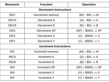
5.8 Decrement and Increment Instructions. . . .65
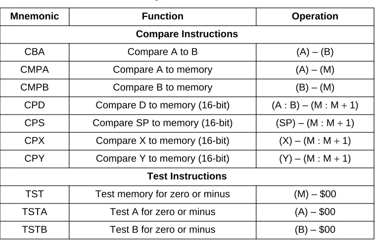
5.9 Compare and Test Instructions. . . .66
5.10 Boolean Logic Instructions . . . .67
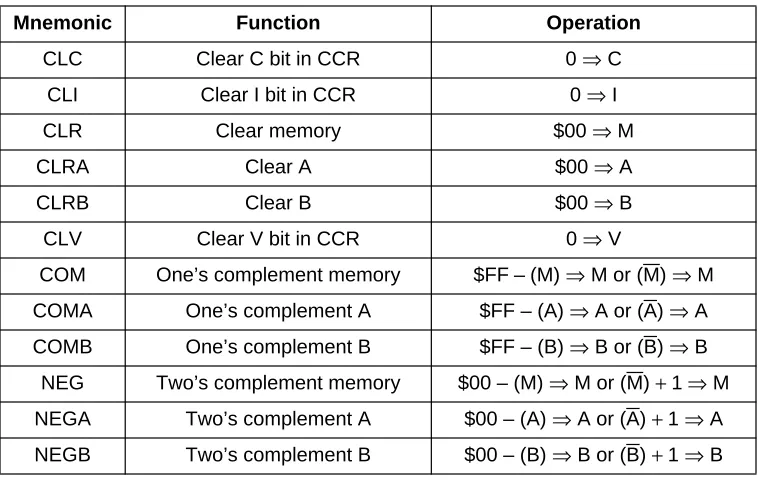
5.11 Clear, Complement, and Negate Instructions. . . .68
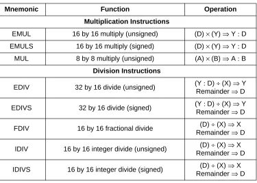
5.12 Multiplication and Division Instructions . . . .69
5.13 Bit Test and Manipulation Instructions . . . .70
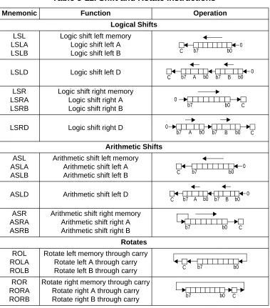
5.14 Shift and Rotate Instructions. . . .71
5.15 Fuzzy Logic Instructions . . . .72
5.15.1 Fuzzy Logic Membership Instruction . . . .72
5.15.2 Fuzzy Logic Rule Evaluation Instructions. . . .72
Reference Manual S12CPUV2
10 Table of Contents MOTOROLA
Table of Contents
5.16 Maximum and Minimum Instructions . . . .75
5.17 Multiply and Accumulate Instruction . . . .76
5.18 Table Interpolation Instructions. . . .76
5.19 Branch Instructions . . . .77
5.19.1 Short Branch Instructions . . . .78
5.19.2 Long Branch Instructions . . . .79
5.19.3 Bit Condition Branch Instructions . . . .80
5.20 Loop Primitive Instructions . . . .81
5.21 Jump and Subroutine Instructions . . . .82
5.22 Interrupt Instructions . . . .83
5.23 Index Manipulation Instructions . . . .85
5.24 Stacking Instructions. . . .86
5.25 Pointer and Index Calculation Instructions . . . .87
5.26 Condition Code Instructions . . . .88
5.27 Stop and Wait Instructions . . . .89
5.28 Background Mode and Null Operations . . . .90
Section 6. Instruction Glossary
6.1 Introduction . . . .916.2 Glossary Information. . . .92
6.3 Condition Code Changes . . . .93
6.4 Object Code Notation . . . .94
6.5 Source Forms . . . .95
6.6 Cycle-by-Cycle Execution. . . .98
6.7 Glossary . . . .103
Section 7. Exception Processing
7.1 Introduction . . . .3157.2 Types of Exceptions . . . .315
7.3 Exception Priority . . . .316
7.4 Resets. . . .318
[image:10.612.176.560.104.683.2]Table of Contents
7.4.2 External Reset . . . .318
7.4.3 COP Reset . . . .319
7.4.4 Clock Monitor Reset . . . .319
7.5 Interrupts. . . .319
7.5.1 Non-Maskable Interrupt Request (XIRQ) . . . .319
7.5.2 Maskable Interrupts . . . .320
7.5.3 Interrupt Recognition . . . .320
7.5.4 External Interrupts . . . .321
7.5.5 Return-from-Interrupt Instruction (RTI) . . . .321
7.6 Unimplemented Opcode Trap. . . .322
7.7 Software Interrupt Instruction (SWI) . . . .322
7.8 Exception Processing Flow. . . .323
7.8.1 Vector Fetch . . . .323
7.8.2 Reset Exception Processing . . . .323
7.8.3 Interrupt and Unimplemented Opcode Trap Exception Pro-cessing 325
Section 8. Instruction Queue
8.1 Introduction . . . .3278.2 External Reconstruction of the Queue . . . .327
8.3 Instruction Queue Status Signals . . . .328
8.3.1 HCS12 Timing Detail . . . .329
8.3.2 M68HC12 Timing Detail . . . .329
8.3.3 Null (Code 0:0). . . .331
8.3.4 LAT — Latch Data from Bus (Code 0:1) . . . .331
8.3.5 ALD — Advance and Load from Data Bus (Code 1:0) .331 8.3.6 ALL — Advance and Load from Latch (Code 1:1). . . . .331
8.3.7 INT — Interrupt Sequence Start (Code 0:1) . . . .331
8.3.8 SEV — Start Instruction on Even Address (Code 1:0) .332 8.3.9 SOD — Start Instruction on Odd Address (Code 1:1). .332 8.4 Queue Reconstruction (for HCS12) . . . .332
8.4.1 Queue Reconstruction Registers (for HCS12) . . . .333
8.4.1.1 fetch_add Register. . . .333
8.4.1.2 st1_add, st1_dat Registers . . . .333
8.4.1.3 st2_add, st2_dat Registers . . . .333
Reference Manual S12CPUV2
12 Table of Contents MOTOROLA
Table of Contents
8.4.2 Reconstruction Algorithm (for HCS12) . . . .334
8.5 Queue Reconstruction (for M68HC12) . . . .335
8.5.1 Queue Reconstruction Registers (for M68HC12). . . .336
8.5.1.1 in_add, in_dat Registers . . . .336
8.5.1.2 fetch_add, fetch_dat Registers. . . .336
8.5.1.3 st1_add, st1_dat Registers . . . .336
8.5.1.4 st2_add, st2_dat Registers . . . .336
8.5.2 Reconstruction Algorithm (for M68HC12) . . . .337
8.5.2.1 LAT Decoding. . . .337
8.5.2.2 ALD Decoding . . . .338
8.5.2.3 ALL Decoding. . . .338
8.6 Instruction Tagging . . . .339
Section 9. Fuzzy Logic Support
9.1 Introduction . . . .3419.2 Fuzzy Logic Basics . . . .342
9.2.1 Fuzzification (MEM) . . . .344
9.2.2 Rule Evaluation (REV and REVW). . . .346
9.2.3 Defuzzification (WAV) . . . .348
9.3 Example Inference Kernel . . . .349
9.4 MEM Instruction Details . . . .351
9.4.1 Membership Function Definitions . . . .351
9.4.2 Abnormal Membership Function Definitions. . . .353
9.4.2.1 Abnormal Membership Function Case 1 . . . .355
9.4.2.2 Abnormal Membership Function Case 2 . . . .356
9.4.2.3 Abnormal Membership Function Case 3 . . . .356
9.5 REV and REVW Instruction Details . . . .357
9.5.1 Unweighted Rule Evaluation (REV) . . . .357
9.5.1.1 Set Up Prior to Executing REV . . . .357
9.5.1.2 Interrupt Details . . . .359
9.5.1.3 Cycle-by-Cycle Details for REV . . . .359
9.5.2 Weighted Rule Evaluation (REVW) . . . .363
9.5.2.1 Set Up Prior to Executing REVW . . . .363
9.5.2.2 Interrupt Details . . . .365
9.5.2.3 Cycle-by-Cycle Details for REVW . . . .365
Table of Contents
9.6.1 Set Up Prior to Executing WAV . . . .369
9.6.2 WAV Interrupt Details . . . .369
9.6.3 Cycle-by-Cycle Details for WAV and wavr . . . .370
9.7 Custom Fuzzy Logic Programming. . . .374
9.7.1 Fuzzification Variations . . . .374
9.7.2 Rule Evaluation Variations . . . .377
9.7.3 Defuzzification Variations . . . .378
Appendix A. Instruction Reference
A.1 Introduction . . . .381A.2 Stack and Memory Layout . . . .382
A.3 Interrupt Vector Locations. . . .382
A.4 Notation Used in Instruction Set Summary. . . .383
A.5 Hexadecimal to Decimal Conversion . . . .408
A.6 Decimal to Hexadecimal Conversion . . . .408
Appendix B. M68HC11 to CPU12 Upgrade Path
B.1 Introduction . . . .409B.2 CPU12 Design Goals . . . .409
B.3 Source Code Compatibility . . . .410
B.4 Programmer’s Model and Stacking. . . .413
B.5 True 16-Bit Architecture . . . .413
B.5.1 Bus Structures . . . .413
B.5.2 Instruction Queue . . . .414
B.5.3 Stack Function . . . .415
B.6 Improved Indexing . . . .417
B.6.1 Constant Offset Indexing . . . .418
B.6.2 Auto-Increment Indexing . . . .419
B.6.3 Accumulator Offset Indexing . . . .420
B.6.4 Indirect Indexing . . . .420
B.7 Improved Performance . . . .421
B.7.1 Reduced Cycle Counts. . . .421
B.7.2 Fast Math . . . .421
Reference Manual S12CPUV2
14 Table of Contents MOTOROLA
Table of Contents
B.8 Additional Functions . . . .423
B.8.1 Memory-to-Memory Moves . . . .426
B.8.2 Universal Transfer and Exchange . . . .426
B.8.3 Loop Construct . . . .427
B.8.4 Long Branches . . . .427
B.8.5 Minimum and Maximum Instructions . . . .427
B.8.6 Fuzzy Logic Support. . . .428
B.8.7 Table Lookup and Interpolation . . . .428
B.8.8 Extended Bit Manipulation . . . .429
B.8.9 Push and Pull D and CCR . . . .429
B.8.10 Compare SP . . . .429
B.8.11 Support for Memory Expansion . . . .430
Appendix C. High-Level Language Support
C.1 Introduction . . . .431C.2 Data Types . . . .431
C.3 Parameters and Variables . . . .432
C.3.1 Register Pushes and Pulls . . . .432
C.3.2 Allocating and Deallocating Stack Space . . . .433
C.3.3 Frame Pointer. . . .433
C.4 Increment and Decrement Operators . . . .434
C.5 Higher Math Functions . . . .434
C.6 Conditional If Constructs. . . .435
C.7 Case and Switch Statements . . . .435
C.8 Pointers. . . .436
C.9 Function Calls . . . .436
C.10 Instruction Set Orthogonality . . . .437
[image:14.612.176.570.84.579.2]Reference Manual — S12CPUV2
List of Figures
Figure Title Page
2-1 . Programming Model . . . .25
6-1 . Example Glossary Page . . . .92
7-1 . Exception Processing Flow Diagram . . . .324
8-1 . Queue Status Signal Timing (HCS12) . . . .329
8-2 . Queue Status Signal Timing (M68HC12) . . . .330
8-3 . Reset Sequence for HCS12 . . . .335
8-4 . Reset Sequence for M68HC12. . . .338
8-5 . Tag Input Timing. . . .339
9-1 . Block Diagram of a Fuzzy Logic System . . . .343
9-2 . Fuzzification Using Membership Functions . . . .345
9-3 . Fuzzy Inference Engine . . . .349
9-4 . Defining a Normal Membership Function . . . .352
9-5 . MEM Instruction Flow Diagram. . . .354
9-6 . Abnormal Membership Function Case 1 . . . .355
9-7 . Abnormal Membership Function Case 2 . . . .356
9-8 . Abnormal Membership Function Case 3 . . . .356
9-9 . REV Instruction Flow Diagram . . . .360
9-10 . REVW Instruction Flow Diagram . . . .367
9-11 . WAV and wavr Instruction Flow Diagram (for HCS12) . . . . .372
9-12 . WAV and wavr Instruction Flow Diagram (for M68HC12) . .373 9-13 . Endpoint Table Handling . . . .376
Reference Manual S12CPUV2
16 List of Figures MOTOROLA
Reference Manual — S12CPUV2
List of Tables
Table Title Page
Table Title Page
3-1 . M68HC12 Addressing Mode Summary . . . .34
3-2 . Summary of Indexed Operations . . . .40
3-3 . PC Offsets for MOVE Instructions (M68HC12 Only) . . . .46
5-1 . Load and Store Instructions . . . .60
5-2 . Transfer and Exchange Instructions. . . .62
5-3 . Move Instructions . . . .62
5-4 . Addition and Subtraction Instructions . . . .63
5-5 . BCD Instructions. . . .64
5-6 . Decrement and Increment Instructions. . . .65
5-7 . Compare and Test Instructions . . . .66
5-8 . Boolean Logic Instructions . . . .67
5-9 . Clear, Complement, and Negate Instructions. . . .68
5-10 . Multiplication and Division Instructions. . . .69
5-11 . Bit Test and Manipulation Instructions . . . .70
5-12 . Shift and Rotate Instructions . . . .71
5-13 . Fuzzy Logic Instructions . . . .73
5-14 . Minimum and Maximum Instructions . . . .75
5-15 . Multiply and Accumulate Instructions . . . .76
5-16 . Table Interpolation Instructions . . . .77
5-17 . Short Branch Instructions . . . .78
5-18 . Long Branch Instructions . . . .79
5-19 . Bit Condition Branch Instructions . . . .80
5-20 . Loop Primitive Instructions . . . .81
5-21 . Jump and Subroutine Instructions . . . .83
5-22 . Interrupt Instructions. . . .84
5-23 . Index Manipulation Instructions . . . .85
5-24 . Stacking Instructions . . . .86
Reference Manual S12CPUV2
18 List of Tables MOTOROLA
List of Tables
5-26 . Condition Code Instructions . . . .88
5-27 . Stop and Wait Instructions . . . .89
5-28 . Background Mode and Null Operation Instructions . . . .90
7-1 . CPU12 Exception Vector Map . . . .316
7-2 . Stacking Order on Entry to Interrupts . . . .321
8-1 . IPIPE1 and IPIPE0 Decoding (HCS12 and M68HC12) . . .330
8-2 . Tag Pin Function . . . .339
A-1 . Instruction Set Summary . . . .387
A-2 . CPU12 Opcode Map . . . .401
A-3 . Indexed Addressing Mode Postbyte Encoding (xb) . . . .403
A-4 . Indexed Addressing Mode Summary . . . .404
A-5 . Transfer and Exchange Postbyte Encoding . . . .405
A-6 . Loop Primitive Postbyte Encoding (lb) . . . .406
A-7 . Branch/Complementary Branch . . . .406
A-8 . Hexadecimal to ASCII Conversion . . . .407
A-9 . Hexadecimal to/from Decimal Conversion . . . .408
B-1 . Translated M68HC11 Mnemonics . . . .410
B-2 . Instructions with Smaller Object Code . . . .412
B-3 . Comparison of Math Instruction Speeds . . . .422
Reference Manual — S12CPUV2
Section 1. Introduction
1.1 Introduction
This manual describes the features and operation of the core (central processing unit, or CPU, and development support functions) used in all HCS12 microcontrollers. For reference, information is provided for the M68HC12.
1.2 Features
The CPU12 is a high-speed, 16-bit processing unit that has a
programming model identical to that of the industry standard M68HC11 central processor unit (CPU). The CPU12 instruction set is a proper superset of the M68HC11 instruction set, and M68HC11 source code is accepted by CPU12 assemblers with no changes.
• Full 16-bit data paths supports efficient arithmetic operation and high-speed math execution
• Supports instructions with odd byte counts, including many single-byte instructions. This allows much more efficient use of ROM space.
• An instruction queue buffers program information so the CPU has immediate access to at least three bytes of machine code at the start of every instruction.
• Extensive set of indexed addressing capabilities, including: – Using the stack pointer as an indexing register in all indexed
operations
– Using the program counter as an indexing register in all but auto increment/decrement mode
– Accumulator offsets using A, B, or D accumulators
– Automatic index predecrement, preincrement, postdecrement,
Reference Manual S12CPUV2
20 Introduction MOTOROLA
Introduction
1.3 Symbols and Notation
The symbols and notation shown here are used throughout the manual. More specialized notation that applies only to the instruction glossary or instruction set summary are described at the beginning of those
sections.
1.3.1 Abbreviations for System Resources
A — Accumulator A
B — Accumulator B
D — Double accumulator D (A : B)
X — Index register X
Y — Index register Y
SP — Stack pointer
PC — Program counter
CCR — Condition code register
S — STOP instruction control bit
X — Non-maskable interrupt control bit H — Half-carry status bit
I — Maskable interrupt control bit N — Negative status bit
Z — Zero status bit
Introduction Symbols and Notation
1.3.2 Memory and Addressing
M — 8-bit memory location pointed to by the effective
address of the instruction
M : M+1 — 16-bit memory location. Consists of the contents of the
location pointed to by the effective address
concatenated with the contents of the location at the next higher memory address. The most significant byte is at location M.
M~M+3 M(Y)~M(Y+3)
— 32-bit memory location. Consists of the contents of the effective address of the instruction concatenated with the contents of the next three higher memory locations. The most significant byte is at location M or M(Y).
M(X) — Memory locations pointed to by index register X
M(SP) — Memory locations pointed to by the stack pointer
M(Y+3) — Memory locations pointed to by index register Y plus 3
PPAGE — Program overlay page (bank) number for extended
memory (>64 Kbytes).
Page — Program overlay page
XH — High-order byte
XL — Low-order byte
( ) — Content of register or memory location
$ — Hexadecimal value
Reference Manual S12CPUV2
22 Introduction MOTOROLA
Introduction
1.3.3 Operators
+ — Addition – — Subtraction
• — Logical AND
+ — Logical OR (inclusive)
⊕ — Logical exclusive OR
× — Multiplication
÷ — Division
M — Negation. One’s complement (invert each bit of M) : — Concatenate
Example: A : B means the 16-bit value formed by concatenat-ing 8-bit accumulator A with 8-bit accumulator B.
A is in the high-order position.
⇒— Transfer
Example: (A) ⇒ M means the content of accumulator A is
transferred to memory location M.
⇔— Exchange
Example: D ⇔ X means exchange the contents of D with
Introduction Symbols and Notation
1.3.4 Definitions
Logic level 1 is the voltage that corresponds to the true (1) state. Logic level 0 is the voltage that corresponds to the false (0) state. Set refers specifically to establishing logic level 1 on a bit or bits. Cleared refers specifically to establishing logic level 0 on a bit or bits. Asserted means that a signal is in active logic state. An active low signal
changes from logic level 1 to logic level 0 when asserted, and an active high signal changes from logic level 0 to logic level 1.
Negated means that an asserted signal changes logic state. An active
low signal changes from logic level 0 to logic level 1 when negated, and an active high signal changes from logic level 1 to logic level 0.
ADDR is the mnemonic for address bus. DATA is the mnemonic for data bus. LSB means least significant bit or bits. MSB means most significant bit or bits. LSW means least significant word or words. MSW means most significant word or words.
A specific bit location within a range is referred to by mnemonic and
number. For example, A7 is bit 7 of accumulator A.
A range of bit locations is referred to by mnemonic and the numbers
Reference Manual S12CPUV2
24 Introduction MOTOROLA
Reference Manual — S12CPUV2
Section 2. Overview
2.1 Introduction
This section describes the CPU12 programming model, register set, the data types used, and basic memory organization.
2.2 Programming Model
The CPU12 programming model, shown inFigure 2-1, is the same as
that of the M68HC11 CPU. The CPU has two 8-bit general-purpose accumulators (A and B) that can be concatenated into a single 16-bit accumulator (D) for certain instructions. It also has:
• Two index registers (X and Y)
• 16-bit stack pointer (SP)
• 16-bit program counter (PC)
• 8-bit condition code register (CCR)
Figure 2-1. Programming Model
7
15
15
15
15
15
D
IX
IY
SP
PC
A B
N
S X H I Z V C
0
0
0
0
0
0 7
0
CONDITION CODE REGISTER 8-BIT ACCUMULATORS A AND B
16-BIT DOUBLE ACCUMULATOR D
INDEX REGISTER X
INDEX REGISTER Y
STACK POINTER
Reference Manual S12CPUV2
26 Overview MOTOROLA
Overview
2.2.1 Accumulators
General-purpose 8-bit accumulators A and B are used to hold operands and results of operations. Some instructions treat the combination of these two 8-bit accumulators (A : B) as a 16-bit double accumulator (D).
Most operations can use accumulator A or B interchangeably. However, there are a few exceptions. Add, subtract, and compare instructions involving both A and B (ABA, SBA, and CBA) only operate in one direction, so it is important to make certain the correct operand is in the correct accumulator. The decimal adjust accumulator A (DAA)
instruction is used after binary-coded decimal (BCD) arithmetic
operations. There is no equivalent instruction to adjust accumulator B.
2.2.2 Index Registers
16-bit index registers X and Y are used for indexed addressing. In the indexed addressing modes, the contents of an index register are added to 5-bit, 9-bit, or 16-bit constants or to the content of an accumulator to form the effective address of the instruction operand. The second index register is especially useful for moves and in cases where operands from two separate tables are used in a calculation.
2.2.3 Stack Pointer
The CPU12 supports an automatic program stack. The stack is used to save system context during subroutine calls and interrupts and can also be used for temporary data storage. The stack can be located anywhere in the standard 64-Kbyte address space and can grow to any size up to the total amount of memory available in the system.
The stack pointer (SP) holds the 16-bit address of the last stack location used. Normally, the SP is initialized by one of the first instructions in an application program. The stack grows downward from the address pointed to by the SP. Each time a byte is pushed onto the stack, the stack pointer is automatically decremented, and each time a byte is pulled from the stack, the stack pointer is automatically incremented.
Overview Programming Model
instruction is executed at the end of a subroutine. The return instruction loads the program counter with the previously stacked return address and execution continues at that address.
When an interrupt occurs, the current instruction finishes execution. The address of the next instruction is calculated and pushed onto the stack, all the CPU registers are pushed onto the stack, the program counter is loaded with the address pointed to by the interrupt vector, and execution continues at that address. The stacked registers are referred to as an interrupt stack frame. The CPU12 stack frame is the same as that of the M68HC11.
NOTE: These instructions can be interrupted, and they resume execution once the interrupt has been serviced:
• REV (fuzzy logic rule evaluation)
• REVW (fuzzy logic rule evaluation (weighted)) • WAV (weighted average)
2.2.4 Program Counter
The program counter (PC) is a 16-bit register that holds the address of the next instruction to be executed. It is automatically incremented each time an instruction is fetched.
2.2.5 Condition Code Register
The condition code register (CCR), named for its five status indicators, contains:
Reference Manual S12CPUV2
28 Overview MOTOROLA
Overview
The status bits reflect the results of CPU operation as it executes instructions. The five flags are:
• Half carry (H)
• Negative (N)
• Zero (Z)
• Overflow (V)
• Carry/borrow (C)
The half-carry flag is used only for BCD arithmetic operations. The N, Z, V, and C status bits allow for branching based on the results of a previous operation.
In some architectures, only a few instructions affect condition codes, so that multiple instructions must be executed in order to load and test a variable. Since most CPU12 instructions automatically update condition codes, it is rarely necessary to execute an extra instruction for this purpose. The challenge in using the CPU12 lies in finding instructions that do not alter the condition codes. The most important of these instructions are pushes, pulls, transfers, and exchanges.
It is always a good idea to refer to an instruction set summary (see
Appendix A. Instruction Reference) to check which condition codes are affected by a particular instruction.
The following paragraphs describe normal uses of the condition codes. There are other, more specialized uses. For instance, the C status bit is used to enable weighted fuzzy logic rule evaluation. Specialized usages are described in the relevant portions of this manual and inSection 6. Instruction Glossary.
2.2.5.1 S Control Bit
Overview Programming Model
2.2.5.2 X Mask Bit
The XIRQ input is an updated version of the NMI input found on earlier generations of MCUs. Non-maskable interrupts are typically used to deal with major system failures, such as loss of power. However, enabling non-maskable interrupts before a system is fully powered and initialized can lead to spurious interrupts. The X bit provides a mechanism for enabling non-maskable interrupts after a system is stable.
By default, the X bit is set to 1 during reset. As long as the X bit remains set, interrupt service requests made via the XIRQ pin are not
recognized. An instruction must clear the X bit to enable non-maskable interrupt service requests made via the XIRQ pin. Once the X bit has been cleared to 0, software cannot reset it to 1 by writing to the CCR. The X bit is not affected by maskable interrupts.
When an XIRQ interrupt occurs after non-maskable interrupts are enabled, both the X bit and the I bit are set automatically to prevent other interrupts from being recognized during the interrupt service routine. The mask bits are set after the registers are stacked, but before the interrupt vector is fetched.
Normally, a return-from-interrupt (RTI) instruction at the end of the interrupt service routine restores register values that were present before the interrupt occurred. Since the CCR is stacked before the X bit is set, the RTI normally clears the X bit, and thus re-enables
non-maskable interrupts. While it is possible to manipulate the stacked value of X so that X is set after an RTI, there is no software method to reset X (and disable XIRQ) once X has been cleared.
2.2.5.3 H Status Bit
Reference Manual S12CPUV2
30 Overview MOTOROLA
Overview
2.2.5.4 I Mask Bit
The I bit enables and disables maskable interrupt sources. By default, the I bit is set to 1 during reset. An instruction must clear the I bit to enable maskable interrupts. While the I bit is set, maskable interrupts can become pending and are remembered, but operation continues uninterrupted until the I bit is cleared.
When an interrupt occurs after interrupts are enabled, the I bit is automatically set to prevent other maskable interrupts during the interrupt service routine. The I bit is set after the registers are stacked, but before the first instruction in the interrupt service routine is executed.
Normally, an RTI instruction at the end of the interrupt service routine restores register values that were present before the interrupt occurred. Since the CCR is stacked before the I bit is set, the RTI normally clears the I bit, and thus re-enables interrupts. Interrupts can be re-enabled by clearing the I bit within the service routine, but implementing a nested interrupt management scheme requires great care and seldom improves system performance.
2.2.5.5 N Status Bit
The N bit shows the state of the MSB of the result. N is most commonly used in two’s complement arithmetic, where the MSB of a negative number is 1 and the MSB of a positive number is 0, but it has other uses. For instance, if the MSB of a register or memory location is used as a status flag, the user can test status by loading an accumulator.
2.2.5.6 Z Status Bit
The Z bit is set when all the bits of the result are 0s. Compare
instructions perform an internal implied subtraction, and the condition codes, including Z, reflect the results of that subtraction. The increment index register X (INX), decrement index register X (DEX), increment index register Y (INY), and decrement index register Y (DEY)
Overview Data Types
2.2.5.7 V Status Bit
The V bit is set when two’s complement overflow occurs as a result of an operation.
2.2.5.8 C Status Bit
The C bit is set when a carry occurs during addition or a borrow occurs during subtraction. The C bit also acts as an error flag for multiply and divide operations. Shift and rotate instructions operate through the C bit to facilitate multiple-word shifts.
2.3 Data Types
The CPU12 uses these types of data: • Bits
• 5-bit signed integers
• 8-bit signed and unsigned integers
• 8-bit, 2-digit binary-coded decimal numbers • 9-bit signed integers
• 16-bit signed and unsigned integers
• 16-bit effective addresses
• 32-bit signed and unsigned integers
Negative integers are represented in two’s complement form.
Five-bit and 9-bit signed integers are used only as offsets for indexed addressing modes.
Sixteen-bit effective addresses are formed during addressing mode computations.
Thirty-two-bit integer dividends are used by extended division
Reference Manual S12CPUV2
32 Overview MOTOROLA
Overview
2.4 Memory Organization
The standard CPU12 address space is 64 Kbytes. Some M68HC12 devices support a paged memory expansion scheme that increases the standard space by means of predefined windows in address space. The CPU12 has special instructions that support use of expanded memory.
Eight-bit values can be stored at any odd or even byte address in available memory.
Sixteen-bit values are stored in memory as two consecutive bytes; the high byte occupies the lowest address, but need not be aligned to an even boundary.
Thirty-two-bit values are stored in memory as four consecutive bytes; the high byte occupies the lowest address, but need not be aligned to an even boundary.
All input/output (I/O) and all on-chip peripherals are memory-mapped. No special instruction syntax is required to access these addresses. On-chip registers and memory typically are grouped in blocks which can be relocated within the standard 64-Kbyte address space. Refer to device documentation for specific information.
2.5 Instruction Queue
The CPU12 uses an instruction queue to buffer program information. The mechanism is called a queue rather than a pipeline because a typical pipelined CPU executes more than one instruction at the same time, while the CPU12 always finishes executing an instruction before beginning to execute another. Refer toSection 4. Instruction Queue
Reference Manual — S12CPUV2
Section 3. Addressing Modes
3.1 Introduction
Addressing modes determine how the central processor unit (CPU) accesses memory locations to be operated upon. This section discusses the various modes and how they are used.
3.2 Mode Summary
Addressing modes are an implicit part of CPU12 instructions. Refer to
Appendix A. Instruction Reference for the modes used by each instruction. All CPU12 addressing modes are shown inTable 3-1.
The CPU12 uses all M68HC11 modes as well as new forms of indexed addressing. Differences between M68HC11 and M68HC12 indexed modes are described in 3.9 Indexed Addressing Modes. Instructions that use more than one mode are discussed in 3.10 Instructions Using
Multiple Modes.
3.3 Effective Address
Reference Manual S12CPUV2
34 Addressing Modes MOTOROLA
Addressing Modes
Table 3-1. M68HC12 Addressing Mode Summary
Addressing Mode Source Format Abbreviation Description
Inherent
INST
(no externally supplied operands)
INH Operands (if any) are in CPU registers
Immediate
INST #opr8i or
INST #opr16i
IMM Operand is included in instruction stream 8- or 16-bit size implied by context
Direct INSTopr8a DIR Operand is the lower 8 bits of an address in the range $0000–$00FF
Extended INSTopr16a EXT Operand is a 16-bit address Relative
INSTrel8 or
INSTrel16
REL An 8-bit or 16-bit relative offset from the current pc is supplied in the instruction
Indexed
(5-bit offset) INSToprx5,xysp IDX
5-bit signed constant offset from X, Y, SP, or PC Indexed
(pre-decrement) INSToprx3,–xys IDX Auto pre-decrement x, y, or sp by 1 ~ 8 Indexed
(pre-increment) INSToprx3,+xys IDX Auto pre-increment x, y, or sp by 1 ~ 8 Indexed
(post-decrement) INSToprx3,xys– IDX Auto post-decrement x, y, or sp by 1 ~ 8 Indexed
(post-increment) INSToprx3,xys+ IDX Auto post-increment x, y, or sp by 1 ~ 8 Indexed
(accumulator offset) INSTabd,xysp IDX
Indexed with 8-bit (A or B) or 16-bit (D) accumulator offset from X, Y, SP, or PC Indexed
(9-bit offset) INSToprx9,xysp IDX1
9-bit signed constant offset from X, Y, SP, or PC (lower 8 bits of offset in one extension byte) Indexed
(16-bit offset) INSToprx16,xysp IDX2
16-bit constant offset from X, Y, SP, or PC (16-bit offset in two extension bytes) Indexed-Indirect
(16-bit offset) INST [oprx16,xysp] [IDX2]
Pointer to operand is found at...
16-bit constant offset from X, Y, SP, or PC (16-bit offset in two extension bytes) Indexed-Indirect
(D accumulator offset) INST [D,xysp] [D,IDX]
Addressing Modes Inherent Addressing Mode
3.4 Inherent Addressing Mode
Instructions that use this addressing mode either have no operands or all operands are in internal CPU registers. In either case, the CPU does not need to access any memory locations to complete the instruction.
Examples:
NOP ;this instruction has no operands
INX ;operand is a CPU register
3.5 Immediate Addressing Mode
Operands for immediate mode instructions are included in the instruction stream and are fetched into the instruction queue one 16-bit word at a time during normal program fetch cycles. Since program data is read into the instruction queue several cycles before it is needed, when an immediate addressing mode operand is called for by an instruction, it is already present in the instruction queue.
The pound symbol (#) is used to indicate an immediate addressing mode operand. One common programming error is to accidentally omit the # symbol. This causes the assembler to misinterpret the expression that follows it as an address rather than explicitly provided data. For
example, LDAA #$55 means to load the immediate value $55 into the A accumulator, while LDAA $55 means to load the value from address $0055 into the A accumulator. Without the # symbol, the instruction is erroneously interpreted as a direct addressing mode instruction.
Examples:
LDAA #$55
LDX #$1234
LDY #$67
These are common examples of 8-bit and 16-bit immediate addressing modes. The size of the immediate operand is implied by the instruction context. In the third example, the instruction implies a 16-bit immediate value but only an 8-bit value is supplied. In this case the assembler will generate the 16-bit value $0067 because the CPU expects a 16-bit value in the instruction stream.
Example:
Reference Manual S12CPUV2
36 Addressing Modes MOTOROLA
Addressing Modes
In this example, extended addressing mode is used to access the operand FOO, immediate addressing mode is used to access the mask value $03, and relative addressing mode is used to identify the
destination address of a branch in case the branch-taken conditions are met. BRSET is listed as an extended mode instruction even though immediate and relative modes are also used.
3.6 Direct Addressing Mode
This addressing mode is sometimes called zero-page addressing because it is used to access operands in the address range $0000 through $00FF. Since these addresses always begin with $00, only the eight low-order bits of the address need to be included in the instruction, which saves program space and execution time. A system can be optimized by placing the most commonly accessed data in this area of memory. The eight low-order bits of the operand address are supplied with the instruction, and the eight high-order bits of the address are assumed to be 0.
Example:
LDAA $55
This is a basic example of direct addressing. The value $55 is taken to be the low-order half of an address in the range $0000 through $00FF. The high order half of the address is assumed to be 0. During execution of this instruction, the CPU combines the value $55 from the instruction with the assumed value of $00 to form the address $0055, which is then used to access the data to be loaded into accumulator A.
Example:
LDX $20
Addressing Modes Extended Addressing Mode
3.7 Extended Addressing Mode
In this addressing mode, the full 16-bit address of the memory location to be operated on is provided in the instruction. This addressing mode can be used to access any location in the 64-Kbyte memory map.
Example:
LDAA $F03B
This is a basic example of extended addressing. The value from address $F03B is loaded into the A accumulator.
3.8 Relative Addressing Mode
The relative addressing mode is used only by branch instructions. Short and long conditional branch instructions use relative addressing mode exclusively, but branching versions of bit manipulation instructions (branch if bits set (BRSET) and branch if bits cleared (BRCLR)) use multiple addressing modes, including relative mode. Refer to
3.10 Instructions Using Multiple Modes for more information.
Short branch instructions consist of an 8-bit opcode and a signed 8-bit offset contained in the byte that follows the opcode. Long branch instructions consist of an 8-bit prebyte, an 8-bit opcode, and a signed 16-bit offset contained in the two bytes that follow the opcode.
Each conditional branch instruction tests certain status bits in the condition code register. If the bits are in a specified state, the offset is added to the address of the next memory location after the offset to form an effective address, and execution continues at that address. If the bits are not in the specified state, execution continues with the instruction immediately following the branch instruction.
Reference Manual S12CPUV2
38 Addressing Modes MOTOROLA
Addressing Modes
continues with the instruction immediately following the branch instruction.
8-bit, 9-bit, and 16-bit offsets are signed two’s complement numbers to support branching upward and downward in memory. The numeric range of short branch offset values is $80 (–128) to $7F (127). Loop primitive instructions support a 9-bit offset which allows a range of $100 (–256) to $0FF (255). The numeric range of long branch offset values is $8000 (–32,768) to $7FFF (32,767). If the offset is 0, the CPU executes the instruction immediately following the branch instruction, regardless of the test involved.
Since the offset is at the end of a branch instruction, using a negative offset value can cause the program counter (PC) to point to the opcode and initiate a loop. For instance, a branch always (BRA) instruction consists of two bytes, so using an offset of $FE sets up an infinite loop; the same is true of a long branch always (LBRA) instruction with an offset of $FFFC.
An offset that points to the opcode can cause a bit-condition branch to repeat execution until the specified bit condition is satisfied. Since bit-condition branches can consist of four, five, or six bytes depending on the addressing mode used to access the byte in memory, the offset value that sets up a loop can vary. For instance, using an offset of $FC with a BRCLR that accesses memory using an 8-bit indexed postbyte sets up a loop that executes until all the bits in the specified memory byte that correspond to 1s in the mask byte are cleared.
3.9 Indexed Addressing Modes
Addressing Modes Indexed Addressing Modes
The indexed addressing scheme uses a postbyte plus zero, one, or two extension bytes after the instruction opcode. The postbyte and
extensions do the following tasks:
1. Specify which index register is used
2. Determine whether a value in an accumulator is used as an offset
3. Enable automatic pre- or post-increment or pre- or post-decrement
4. Specify size of increment or decrement
5. Specify use of 5-, 9-, or 16-bit signed offsets
This approach eliminates the differences between X and Y register use while dramatically enhancing the indexed addressing capabilities.
Major advantages of the CPU12 indexed addressing scheme are: • The stack pointer can be used as an index register in all indexed
operations.
• The program counter can be used as an index register in all but autoincrement and autodecrement modes.
• A, B, or D accumulators can be used for accumulator offsets. • Automatic pre- or post-increment or pre- or post-decrement by –8
to +8
• A choice of 5-, 9-, or 16-bit signed constant offsets
• Use of two new indexed-indirect modes:
– Indexed-indirect mode with 16-bit offset
– Indexed-indirect mode with accumulator D offset
Table 3-2is a summary of indexed addressing mode capabilities and a description of postbyte encoding. The postbyte is noted as xb in
instruction descriptions. Detailed descriptions of the indexed addressing mode variations follow the table.
Reference Manual S12CPUV2
40 Addressing Modes MOTOROLA
Addressing Modes
Indexed addressing mode instructions use a postbyte to specify index registers (X and Y), stack pointer (SP), or program counter (PC) as the base index register and to further classify the way the effective address is formed. A special group of instructions cause this calculated effective address to be loaded into an index register for further calculations:
• Load stack pointer with effective address (LEAS)
• Load X with effective address (LEAX)
[image:40.612.57.561.99.526.2]• Load Y with effective address (LEAY)
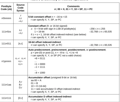
Table 3-2. Summary of Indexed Operations
Postbyte Code (xb) Source Code Syntax Comments
rr; 00 = X, 01 = Y, 10 = SP, 11 = PC
rr0nnnnn
,r n,r –n,r
5-bit constant offset n = –16 to +15
r can specify X, Y, SP, or PC
111rr0zs n,r –n,r
Constant offset (9- or 16-bit signed)
z- 0 = 9-bit with sign in LSB of postbyte(s) –256≤ n≤ 255
1 = 16-bit –32,768≤ n≤ 65,535
if z = s = 1, 16-bit offset indexed-indirect (see below) r can specify X, Y, SP, or PC
111rr011 [n,r] 16-bit offset indexed-indirect
rr can specify X, Y, SP, or PC –32,768≤ n≤ 65,535
rr1pnnnn
n,–r n,+r n,r– n,r+
Auto predecrement, preincrement, postdecrement, or postincrement;
p = pre-(0) or post-(1), n = –8 to –1, +1 to +8 r can specify X, Y, or SP (PC not a valid choice)
+8 = 0111 …
+1 = 0000 –1 = 1111 …
–8 = 1000
111rr1aa
A,r B,r D,r
Accumulator offset (unsigned 8-bit or 16-bit)
aa-00 = A 01 = B
10 = D (16-bit)
11 = see accumulator D offset indexed-indirect r can specify X, Y, SP, or PC
Addressing Modes Indexed Addressing Modes
3.9.1 5-Bit Constant Offset Indexed Addressing
This indexed addressing mode uses a 5-bit signed offset which is included in the instruction postbyte. This short offset is added to the base index register (X, Y, SP, or PC) to form the effective address of the memory location that will be affected by the instruction. This gives a range of–16 through +15 from the value in the base index register.
Although other indexed addressing modes allow 9- or 16-bit offsets, those modes also require additional extension bytes in the instruction for this extra information. The majority of indexed instructions in real programs use offsets that fit in the shortest 5-bit form of indexed addressing.
Examples:
LDAA 0,X
STAB –8,Y
For these examples, assume X has a value of $1000 and Y has a value of $2000 before execution. The 5-bit constant offset mode does not change the value in the index register, so X will still be $1000 and Y will still be $2000 after execution of these instructions. In the first example, A will be loaded with the value from address $1000. In the second example, the value from the B accumulator will be stored at address $1FF8 ($2000 –$8).
3.9.2 9-Bit Constant Offset Indexed Addressing
This indexed addressing mode uses a 9-bit signed offset which is added to the base index register (X, Y, SP, or PC) to form the effective address of the memory location affected by the instruction. This gives a range of
–256 through +255 from the value in the base index register. The most
significant bit (sign bit) of the offset is included in the instruction postbyte and the remaining eight bits are provided as an extension byte after the instruction postbyte in the instruction flow.
Examples:
LDAA $FF,X
LDAB –20,Y
For these examples, assume X is $1000 and Y is $2000 before execution of these instructions.
Reference Manual S12CPUV2
42 Addressing Modes MOTOROLA
Addressing Modes
The first instruction will load A with the value from address $10FF and the second instruction will load B with the value from address $1FEC.
This variation of the indexed addressing mode in the CPU12 is similar to the M68HC11 indexed addressing mode, but is functionally enhanced. The M68HC11 CPU provides for unsigned 8-bit constant offset indexing from X or Y, and use of Y requires an extra instruction byte and thus, an extra execution cycle. The 9-bit signed offset used in the CPU12 covers the same range of positive offsets as the M68HC11, and adds negative offset capability. The CPU12 can use X, Y, SP, or PC as the base index register.
3.9.3 16-Bit Constant Offset Indexed Addressing
This indexed addressing mode uses a 16-bit offset which is added to the base index register (X, Y, SP, or PC) to form the effective address of the memory location affected by the instruction. This allows access to any address in the 64-Kbyte address space. Since the address bus and the offset are both 16 bits, it does not matter whether the offset value is considered to be a signed or an unsigned value ($FFFF may be thought of as +65,535 or as–1). The 16-bit offset is provided as two extension
bytes after the instruction postbyte in the instruction flow.
3.9.4 16-Bit Constant Indirect Indexed Addressing
This indexed addressing mode adds a 16-bit instruction-supplied offset to the base index register to form the address of a memory location that contains a pointer to the memory location affected by the instruction. The instruction itself does not point to the address of the memory location to be acted upon, but rather to the location of a pointer to the address to be acted on. The square brackets distinguish this addressing mode from 16-bit constant offset indexing.
Example:
LDAA [10,X]
Addressing Modes Indexed Addressing Modes
3.9.5 Auto Pre/Post Decrement/Increment Indexed Addressing
This indexed addressing mode provides four ways to automatically change the value in a base index register as a part of instruction
execution. The index register can be incremented or decremented by an integer value either before or after indexing takes place. The base index register may be X, Y, or SP. (Auto-modify modes would not make sense on PC.)
Pre-decrement and pre-increment versions of the addressing mode adjust the value of the index register before accessing the memory location affected by the instruction — the index register retains the changed value after the instruction executes. Post-decrement and post-increment versions of the addressing mode use the initial value in the index register to access the memory location affected by the
instruction, then change the value of the index register.
The CPU12 allows the index register to be incremented or decremented by any integer value in the ranges –8 through –1 or 1 through 8. The value need not be related to the size of the operand for the current instruction. These instructions can be used to incorporate an index adjustment into an existing instruction rather than using an additional instruction and increasing execution time. This addressing mode is also used to perform operations on a series of data structures in memory.
When an LEAS, LEAX, or LEAY instruction is executed using this addressing mode, and the operation modifies the index register that is being loaded, the final value in the register is the value that would have been used to access a memory operand. (Premodification is seen in the result but postmodification is not.)
Examples:
STAA 1,–SP ;equivalent to PSHA
STX 2,–SP ;equivalent to PSHX
LDX 2,SP+ ;equivalent to PULX
LDAA 1,SP+ ;equivalent to PULA
For a “last-used” type of stack like the CPU12 stack, these four examples are equivalent to common push and pull instructions.
Reference Manual S12CPUV2
44 Addressing Modes MOTOROLA
Addressing Modes
stack (PSHX) and pull register X from stack (PULX) require multiple instructions to decrement the SP by one, then store X, then decrement SP by one again.
In the STAA 1,–SP example, the stack pointer is pre-decremented by one and then A is stored to the address contained in the stack pointer. Similarly the LDX 2,SP+ first loads X from the address in the stack pointer, then post-increments SP by two.
Example:
MOVW 2,X+,4,+Y
This example demonstrates how to work with data structures larger than bytes and words. With this instruction in a program loop, it is possible to move words of data from a list having one word per entry into a second table that has four bytes per table element. In this example the source pointer is updated after the data is read from memory (post-increment) while the destination pointer is updated before it is used to access memory (pre-increment).
3.9.6 Accumulator Offset Indexed Addressing
In this indexed addressing mode, the effective address is the sum of the values in the base index register and an unsigned offset in one of the accumulators. The value in the index register itself is not changed. The index register can be X, Y, SP, or PC and the accumulator can be either of the 8-bit accumulators (A or B) or the 16-bit D accumulator.
Example:
LDAA B,X
This instruction internally adds B to X to form the address from which A will be loaded. B and X are not changed by this instruction. This example is similar to the following 2-instruction combination in an M68HC11.
Examples:
ABX
LDAA 0,X
Addressing Modes Instructions Using Multiple Modes
3.9.7 Accumulator D Indirect Indexed Addressing
This indexed addressing mode adds the value in the D accumulator to the value in the base index register to form the address of a memory location that contains a pointer to the memory location affected by the instruction. The instruction operand does not point to the address of the memory location to be acted upon, but rather to the location of a pointer to the address to be acted upon. The square brackets distinguish this addressing mode from D accumulator offset indexing.
Examples:
JMP [D,PC]
GO1 DC.W PLACE1
GO2 DC.W PLACE2
GO3 DC.W PLACE3
This example is a computed GOTO. The values beginning at GO1 are addresses of potential destinations of the jump (JMP) instruction. At the time the JMP [D,PC] instruction is executed, PC points to the address GO1, and D holds one of the values $0000, $0002, or $0004
(determined by the program some time before the JMP).
Assume that the value in D is $0002. The JMP instruction adds the values in D and PC to form the address of GO2. Next the CPU reads the address PLACE2 from memory at GO2 and jumps to PLACE2. The locations of PLACE1 through PLACE3 were known at the time of program assembly but the destination of the JMP depends upon the value in D computed during program execution.
3.10 Instructions Using Multiple Modes
Several CPU12 instructions use more than one addressing mode in the course of execution.
3.10.1 Move Instructions
Move instructions use separate addressing modes to access the source and destination of a move. There are move variations for all practical combinations of immediate, extended, and indexed addressing modes.
Reference Manual S12CPUV2
46 Addressing Modes MOTOROLA
Addressing Modes
Move instructions do not support indirect modes, 9-bit, or 16-bit offset modes requiring extra extension bytes. There are special considerations when using PC-relative addressing with move instructions. The original M68HC12 implemented the instruction queue slightly differently than the newer HCS12. In the older M68HC12 implementation, the CPU did not maintain a pointer to the start of the instruction after the current
instruction (what the user thinks of as the PC value during execution). This caused an offset for PC-relative move instructions.
PC-relative addressing uses the address of the location immediately following the last byte of object code for the current instruction as a reference point. The CPU12 normally corrects for queue offset and for instruction alignment so that queue operation is transparent to the user. However, in the original M68HC12, move instructions pose three special problems:
• Some moves use an indexed source and an indexed destination.
• Some moves have object code that is too long to fit in the queue all at one time, so the PC value changes during execution. • All moves do not have the indexed postbyte as the last byte of
object code.
These cases are not handled by automatic queue pointer maintenance, but it is still possible to use PC-relative indexing with move instructions by providing for PC offsets in source code.
Table 3-3shows PC offsets from the location immediately following the current instruction by addressing mode.
Table 3-3. PC Offsets for MOVE Instructions (M68HC12 Only)
MOVE Instruction Addressing Modes Offset Value
MOVB
IMM⇒IDX +1
EXT⇒IDX +2
IDX⇒EXT –2
IDX⇒IDX –1 for first operand +1 for second operand
MOVW
IMM⇒IDX +2
EXT⇒IDX +2
IDX⇒EXT –2
Addressing Modes Instructions Using Multiple Modes
Example:
1000 18 09 C2 20 00 MOVB $2000 2,PC
Moves a byte of data from $2000 to $1009
The expected location of the PC = $1005. The offset = +2. [1005 + 2 (for 2,PC) + 2 (for correction) = 1009]
$18 is the page pre-byte, 09 is the MOVB opcode for ext-idx, C2 is the indexed postbyte for 2,PC (without correction).
The Motorola MCUasm assembler produces corrected object code for PC-relative moves (18 09 C0 20 00 for the example shown).
NOTE: Instead of assembling the 2,PC as C2, the correction has been applied to make it C0. Check whether an assembler makes the correction before using PC-relative moves.
On the newer HCS12, the instruction queue was implemented such that an internal pointer, to the start of the next instruction, is always available. On the HCS12, PC-relative move instructions work as expected without any offset adjustment. Although this is different from the original
M68HC12, it is unlikely to be a problem because PC-relative indexing is rarely, if ever, used with move instructions.
3.10.2 Bit Manipulation Instructions
Bit manipulation instructions use either a combination of two or a combination of three addressing modes.
The clear bits in memory (BCLR) and set bits in memory (BSET)
instructions use an 8-bit mask to determine which bits in a memory byte are to be changed. The mask must be supplied with the instruction as an immediate mode value. The memory location to be modified can be specified by means of direct, extended, or indexed addressing modes.
Reference Manual S12CPUV2
48 Addressing Modes MOTOROLA
Addressing Modes
3.11 Addressing More than 64 Kbytes
Some M68HC12 devices incorporate hardware that supports
addressing a larger memory space than the standard 64 Kbytes. The expanded memory system uses fast on-chip logic to implement a transparent bank-switching scheme.
Increased code efficiency is the greatest advantage of using a switching scheme instead of a large linear address space. In systems with large linear address spaces, instructions require more bits of information to address a memory location, and CPU overhead is greater. Other advantages include the ability to change the size of system memory and the ability to use various types of external memory.
However, the add-on bank switching schemes used in other
microcontrollers have known weaknesses. These include the cost of external glue logic, increased programming overhead to change banks, and the need to disable interrupts while banks are switched.
The M68HC12 system requires no external glue logic. Bank switching overhead is reduced by implementing control logic in the MCU.
Interrupts do not need to be disabled during switching because switching tasks are incorporated in special instructions that greatly simplify
program access to extended memory.
MCUs with expanded memory treat the 16 Kbytes of memory space from $8000 to $BFFF as a program memory window.
Expanded-memory architecture includes an 8-bit program page register (PPAGE), which allows up to 256 16-Kbyte program memory pages to be switched into and out of the program memory window. This provides for up to 4 Megabytes of paged program memory.
The CPU12 instruction set includes call subroutine in expanded memory (CALL) and return from call (RTC) instructions, which greatly simplify the use of expanded memory space. These instructions also execute correctly on devices that do not have expanded-memory addressing capability, thus providing for portable code.
The CALL instruction is similar to the jump-to-subroutine (JSR) instruction. When CALL is executed, the current value in PPAGE is pushed onto the stack with a return address, and a new
Addressing Modes Addressing More than 64 Kbytes
the effective address. For all addressing mode variations except indexed indirect modes, the new page value is provided by an immediate
operand in the instruction. For indexed indirect variations of CALL, a pointer specifies memory locations where the new page value and the address of the called subroutine are stored. Use of indirect addressing for both the page value and the address within the page frees the program from keeping track of explicit values for either address.
Reference Manual S12CPUV2
50 Addressing Modes MOTOROLA
Reference Manual — S12CPUV2
Section 4. Instruction Queue
4.1 Introduction
The CPU12 uses an instruction queue to increase execution speed. This section describes queue operation during normal program
execution and changes in execution flow. These concepts augment the descriptions of instructions and cycle-by-cycle instruction execution in subsequent sections, but it is important to note that queue operation is automatic, and generally transparent to the user.
The material in this section is general.Section 6. Instruction Glossary
contains detailed information concerning cycle-by-cycle execution of each instruction.Section 8. Instruction Queue contains detailed information about tracking queue operation and instruction execution.
4.2 Queue Description
The fetching mechanism in the CPU12 is best described as a queue rather than as a pipeline. Queue logic fetches program information and positions it for execution, but instructions are executed sequentially. A typical pipelined central processor unit (CPU) can execute more than one instruction at the same time, but interactions between the prefetch and execution mechanisms can make tracking and debugging difficult. The CPU12 thus gains the advantages of independent fetches, yet maintains a straightforward relationship between bus and execution cycles.
Each instruction refills the queue by fetching the same number of bytes that the instruction uses. Program information is fetched in aligned 16-bit words. Each program fetch (P) indicates that two bytes need to be replaced in the instruction queue. Each optional fetch (O) indicates that only one byte needs to be replaced. For example, an instruction
Reference Manual S12CPUV2
52 Instruction Queue MOTOROLA
Instruction Queue
optional fetch is converted into a free cycle. If the first byte was odd-aligned, the optional fetch is executed as a program fetch.
Two external pins, IPIPE[1:0], provide time-multiplexed information about data movement in the queue and instruction execution. Decoding and use of these signals is discussed inSection 8. Instruction Queue.
4.2.1 Original M68HC12 Queue Implementation
There are two 16-bit queue stages and one 16-bit buffer. Program information is fetched in aligned 16-bit words. Unless buffering is required, program information is first queued into stage 1, then advanced to stage 2 for execution.
At least two words of program information are available to the CPU when execution begins. The first byte of object code is in either the even or odd half of the word in stage 2, and at least two more bytes of object code are in the queue.
The buffer is used when a program word arrives before the queue can advance. This occurs during execution of single-byte and odd-aligned instructions. For instance, the queue cannot advance after an aligned, single-byte instruction is executed, because the first byte of the next instruction is also in stage 2. In these cases, information is latched into the buffer until the queue can advance.
4.2.2 HCS12 Queue Implementation
There are three 16-bit stages in the instruction queue. Instructions enter the queue at stage 1 and shift out of stage 3 as the CPU executes instructions and fetches new ones into stage 1. Each byte in the queue is selectable. An opcode prediction algorithm determines the location of the next opcode in the instruction queue.
4.3 Data Movement in the Queue
Instruction Queue Changes in Execution Flow
4.3.1 No Movement
There is no data movement in the instruction queue during the cycle. This occurs during execution of instructions that must perform a number of internal operations, such as division instructions.
4.3.2 Latch Data from Bus (Applies Only to the M68HC12 Queue Implementation)
All instructions initiate fetches to refill the queue as execution proceeds. However, a number of conditions, including instruction alignment and the length of previous instructions, affect when the queue advances. If the queue is not ready to advance when fetched information arrives, the information is latched into the buffer. Later, when the queue does advance, stage 1 is refilled from the buffer. If more than one latch cycle occurs before the queue advances, the buffer is filled on the first latch event and subsequent latch events are ignored until the queue
advances.
4.3.3 Advance and Load from Data Bus
The content of queue is advanced by one stage, and stage 1 is loaded with a word of program information from the data bus. The information was requested two bus cycles earlier but has only become available this cycle, due to access delay.
4.3.4 Advance and Load from Buffer (Applies Only to M68HC12 Queue Implementation)
The content of queue stage 1 advances to stage 2, and stage 1 is loaded with a word of program information from the buffer. The information in the buffer was latched from the data bus during a previous cycle because the queue was not ready to advance when it arrived.
4.4 Changes in Execution Flow
Reference Manual S12CPUV2
54 Instruction Queue MOTOROLA
Instruction Queue
processing, while subroutine calls, branches, and jumps are considered to be elements of program structure.
During design, great care is taken to assure that the mechanism that increases instruction throughput during normal program execution does not cause bottlenecks during changes of program flow, but internal queue operation is largely transparent to the user. The following information is provided to enhance subsequent descriptions of instruction execution.
4.4.1 Exceptions
Exceptions are events that require processing outside the normal flow of instruction execution. CPU12 exceptions include five types of
exceptions:
• Reset (including COP, clock monitor, and pin)
• Unimplemented opcode trap
• Software interrupt instruction • X-bit interrupts
• I-bit interrupts
All exceptions use the same microcode, but the CPU follows different execution paths for each type of exception.
CPU12 exception handling is designed to minimize the effect of queue operation on context switching. Thus, an exception vector fetch is the first part of exception processing, and fetches to refill the queue from the address pointed to by the vector are interleaved with the stacking operations that preserve context, so that program access time does not delay the switch. Refer toSection 7. Exception Processingfor detailed information.
4.4.2 Subroutines
The CPU12 can branch to (BSR), jump to (JSR), or call (CALL)
Instruction Queue Changes in Execution Flow
BSR uses relative addressing mode to generate the effective address of the subroutine, while JSR can use various other addressing modes. Both instructions calculate a return address, stack the address, then perform three program word fetches to refill the queue.
Subroutines in the normal 64-Kbyte address space are terminated with a return-from-subroutine (RTS) instruction. RTS unstacks the return address, then performs three program word fetches from that address to refill the queue.
CALL is similar to JSR. MCUs with expanded memory treat 16 Kbytes of addresses from $8000 to $BFFF as a memory window. An 8-bit PPAGE register switches memory pages into and out of the window. When CALL is executed, a return address is calculated, then it and the current PPAGE value