N A N O E X P R E S S
Open Access
Dual Functions of V/SiO
x
/AlO
y
/p
++
Si Device
as Selector and Memory
Sungjun Kim
1, Chih-Yang Lin
2, Min-Hwi Kim
3, Tae-Hyeon Kim
3, Hyungjin Kim
3, Ying-Chen Chen
4,
Yao-Feng Chang
5*and Byung-Gook Park
3*Abstract
This letter presents dual functions including selector and memory switching in a V/SiOx/AlOy/p++Si resistive memory device by simply controlling compliance current limit (CCL). Unidirectional threshold switching is observed after a positive forming with low CCL of 1μA. The shifts to the V-electrode side of the oxygen form the VOxlayer, where the threshold switching can be explained by the metal-insulation-transition phenomenon. For higher CCL (30μA) applied to the device, a bipolar memory switching is obtained, which is attributed to formation and rupture of the conducting filament in SiOylayer. 1.5-nm-thick AlOylayer with high thermal conductivity plays an important role in lowering the off-current for memory and threshold switching. Through the temperature dependence, high-energy barrier (0.463 eV) in the LRS is confirmed, which can cause nonlinearity in a low-resistance state. The smaller the CCL, the higher the nonlinearity, which provides a larger array size in the cross-point array. The coexistence of memory and threshold switching in accordance with the CCL provides the flexibility to control the device for its intended use.
Keywords:Resistive switching, Selector, Memory, Nonlinearity, Silicon oxide, Vanadium
Background
Resistive random-access memory (RRAM) is one of the promising candidates for the next-generation non-volatile memory technology due to its fast switching speed [1,2], low-power consumption [3–8], multilevel capability [9–15], high scalability [16–20], and 3D stacking abil-ity [21–25]. These properties are especially suitable for storage class memory (SCM) which can fill the per-formance gap between dynamic random-access memory (DRAM) as a main memory and solid-state-drive (SSD) as a storage memory. Even though RRAM device has made much progress in the past years [1–25], there remains, however, a major disadvantage: sneak current through neighboring cells occurs in a high-density cross-point array [26]. The memory device with the selector compo-nent should provide nonlinear current–voltage (I–V) characteristics to overcome this problem [26–35]. Until now, various devices with nonlinear concepts such as complementary resistive switching (CRS) [26], tunnel
barrier [27–33], Ag-based threshold switching [34], diode-type selector [35, 36], ovonic threshold switching (OTS) [37, 38], and metal-insulator-transition (MIT) [39– 43] have been reported. VOxas one of the typical MIT
ma-terials could be widely used in potential applications as op-tical and electrical switching component [40–42]. SiO2 is widely used as a passivation layer in the semiconductor in-dustry. Moreover, Si-rich SiOx(x< 2) can be used as a
re-sistance change layer in RRAM [44–55]. SiOx can be
preferred over many other materials in terms of compatibil-ity with CMOS processes and low cost. SiOx-based RRAM
devices have been reported to act as a mediator of the role of conducting bridges simply by using electrodes such as Cu and Ag with high diffusivity [44–47]. In another case, memory switching is induced by the valence change effect inside the SiOxlayer, which can be explained by generation
of oxygen vacancies or proton exchange model [48–55]. In the unipolar switching where a set operation precedes a re-set, it is sensitive to the ambient atmosphere. The switching performance in the air is significantly degraded [48–53]. On the other hand, filamentary switching without backward-scan effects shows typical unipolar and bipolar switching in various SiOx-based RRAM devices [52–54].
* Correspondence:[email protected];[email protected]
5
Intel Corporation, Hillsboro, USA
3Department of Electrical and Computer Engineering, Inter-University
Semiconductor Research Center (ISRC), Seoul National University, Seoul 08826, South Korea
Full list of author information is available at the end of the article
Here, we present the coexistence of threshold switch-ing and memory switchswitch-ing in V/SiOx/AlOy/p
++
Si device depending on compliance current limit (CCL). The de-vice with silicon bottom electrode (BE) has several ad-vantages compared to the conventional metal electrode. The RRAM device with memory or threshold switching is directly connected to the source or drain side in a transistor, which is a potential application for embedded memory and steep slope device. The overshoot current could be reduced due to the series resistance of Si BE. Moreover, nano-tip of silicon BE through wet etching and the adjustment of the doping concentration in sili-con surface can improve switching performance. The AlOylayer, which is a large band gap with an insulated
property, helps to lower the operating current during threshold and memory switching. The SiOxlayer acts as
memory switching layer at a high CCL, while it serves to supply oxygen to V TE at low CCL, which provides threshold switching.
Methods
V/SiOx/AlOy/p++Si device was fabricated as follows:
Firstly, BF2ions were implanted with an acceleration en-ergy of 40 keV and a dose of 5 × 1015cm−2into a Si sub-strate to heavily doped Si BE. The lattice damage was cured by the annealing process at 1050 °C for 10 min. Heavily doped Si BE had sheet resistance of 30.4 Ω/□. Next, a 1.5-nm-thick AlOy layer was deposited by an
atomic layer deposition (ALD) system using H2O and Al (CH3)3 and a 5.5-nm-thick SiOx layer underwent
plasma-enhanced chemical vapor deposition (PECVD) by reacting 5% SiH4/N2 (160 sccm), N2O (1300 sccm), and N2 (240 sccm) at 300 °C. Subsequently, a 50-nm-thick vanadium (V) top electrode (TE) with a diameter of 100μm was deposited by DC sputtering a V target with Ar gas (30 sccm). Finally, a 50-nm-thick Al as a protective layer was deposited by DC sputtering to prevent further oxidation of V TE. All electrical proper-ties were characterized via the DC voltage sweep and pulse modes using a Keithley 4200-SCS semiconductor parameter analyzer (SPA) and a 4225-PMU ultra-fast current–voltage (I–V) module at room temperature, respectively. For device operation, the TiN BE was grounded and the Ni TE bias was controlled.
Results and Discussion
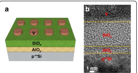
Figure 1a shows the schematic structure of V/SiOx/
AlOy/p++Si device. Three amorphous V, SiOx, and AlOy
layers and single-crystalline Si layer are observed by a transmission electron microscopy (TEM) cross-sectional image as shown in Fig. 1b. The thicknesses of the SiOx
and AlOy layers are 5.5 and 1.5 nm, respectively. To
confirm the composition ratio of two dielectric films, XPS analysis was conducted (Additional file 1). The x
value of SiOxand they value of AlOyare 0.88 and 1.33,
respectively. Our SiOx film using PECVD compared to
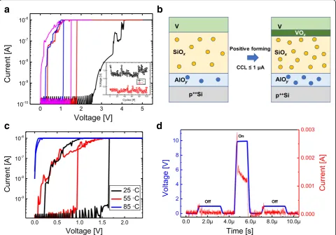
SiO2 deposited using dry oxidation is deposited at a much lower temperature and has much more defects, making them suitable for resistive switching at relatively lower voltages. Figure2ashows typical threshold switch-ing of V/SiOx/AlOy/p++Si device. The initial switching
with a positive forming process requires higher voltage than subsequent threshold switching since the dielectric layers have initially smaller defects. A CCL of 1 μA is applied to the device to avoid the formation of excessive conducting filaments in the SiOx layer. The leakage
current is very low (100 pA at 1 V) compared with previously reported threshold switching of VOx. This
advantage is attributed to the Al2O3with higher permit-tivity and thermal conducpermit-tivity compared to the SiO2. Off-state has the insulating property because the filaments are easily ruptured and then there are no remaining filaments. A possible mechanism for thresh-old switching is the oxidation of the V TE from the oxy-gen supplied from the SiOx layer during the positive
forming process as shown in Fig.2b. The electrical prop-erty of VOx between V TE and SiOx layer may change
from insulating state to metallic state, causing a sudden change in resistance. A low CCL of 1μA is not sufficient to cause efficient conducting filaments inside the SiOx
film. Therefore, SiOx with insulating properties can be
another cause to reduce the off-current. For a negative forming process of V/SiOx/AlOy/p++Si device, a
thresh-old switching is not observed (see Additional file 1). When the negative bias is applied to the V TE, the movement of the oxide moves toward the Si BE, so that the V TE can no longer participate in the threshold switching as VOx. Inset of Fig.2aexhibits the threshold
voltage (Vth) and hold voltage (Vhold) during the 100 -cycles. The Vthwhere the current sharply increases with nearly infinite slope is between 1.08 and 1.82 V, and Vhold at which point the current return to a high-resistance state is between 0.12 and 0.54 V. Figure2cshows the I–V
char-acteristics in the on-current at different temperatures. At
a
b
[image:2.595.306.541.87.212.2]25 °C and 55 °C, they show almost similar threshold switching, but I–V curve at a higher temperature of 85 °C loses the threshold switching property. It is well known that VOx loses its MIT at high temperatures. Thus, this
result is another proof that VOx is the main cause of the
threshold switching. Figure2dshows the transient charac-teristics for threshold switching. The pulse with the ampli-tude of 1 V monitored the read current before and after writing pulse with width of 1 μs. The high current was monitored while the pulse with high amplitude is applied to the device, and then, the V/SiOx/AlOy/p++Si device
turned off the current immediately after the writing pulse was removed. The selector properties analyzed above can be used when combined with operation of memory ele-ments below 1μA [55,56].
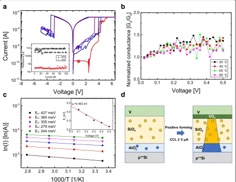
Figure 3a shows the bipolar resistive switching of V/ SiOx/AlOy/p++Si device after a positive forming with
CCL of 100 μA. Then, the reset process with a rapid increase in resistance is performed by sweeping the negative voltage, and the device is switched to a high-resistance state (HRS). The set process with a rapid decrease in resistance then occurs at a positive bias
voltage, causing the device to turn back to a low-resist-ance state (LRS). In order to understand the properties of the conducting filament, we observe the normalized conductance and the temperature dependence. The con-duction in the LRS is an important guideline to indir-ectly inform the properties of the conducting filament. Figure 3b shows the normalized conductance (GN) which is defined as the dynamic conductance (Gd) divide by static conductance (G0) for I–V curves of V/SiOx/
AlOy/p++Si device in the LRS with different
tempera-tures. Regardless of the temperature, the GN value con-verges to 1 when the voltage is zero. This allows us to rule out the well-known conduction mechanism such as Schottky emission, Fowler-Nordheim tunneling, and Child’s law (I~V2
) in space-charge-limited current (SCLC). Metallic ohmic conduction can also be excluded considering temperature dependence as shown in Fig.3c. The decrease in resistance with increasing the temperature suggests that the conducting filament has a semiconducting property. Thus, we can exclude the pene-tration of V into the SiOx layer for the main conducting
filament of V/SiOx/AlOy/p++Si device in LRS. Therefore,
a
b
d
c
Fig. 2Unidirectional threshold switching of V/SiOx/AlOy/p++Si when a positive forming with CCL of 1μA is applied.aTypical I–V curves.
[image:3.595.58.539.89.424.2]the bipolar memory operation of the V/SiOx/AlOy/p++Si
device is dominated by intrinsic switching of SiOx. It is
also confirmed that the positive and negative currents are not that much different suggesting that rather than an interface-type such as Schottky emission, it is dominated by bulk conduction. Taking into account the abovemen-tioned normalized conductance, there are two possible bulk dominant conduction mechanisms. The first one is hopping conduction following the formula:
J ¼qnavoe−qØT=kTeqaV=2dkT
whereq,n,a,øT,vo, anddare the electric charge,
con-centration of space charge, mean of hopping distance, electron barrier height for hopping, intrinsic vibration frequency, and the thickness of dielectric film, respect-ively. TheøTcalculated from the slope of a linear plot of
ln (I) versus 1000/T is 0.463 eV as shown in Fig. 3c. A
value calculated from the relationship between Eaand V is 5.17 nm, indicating the conducting filament formed in the SiOxis not strong and is close to the HRS state. The
other conduction mechanism, the Poole-Frenkel (P-F) emission, was covered in Additional file 1. Based on the above results, the conducting filament model in the memory operation of V/SiOx/AlOy/p++Si device is
depicted in Fig.3d. In the positive forming process, the oxidation process proceeded on the V TE side, but due to the high CCL, a conductive filament can be formed inside the SiOx and AlOy due to the movement of the
oxygen vacancies. During the reset process, the electric field opposite to the forming and set induces oxygen and recombination with the oxygen vacancy, resulting in the rupture of the conductive filament. It is noted that the selector and memory operations are observed in the same cell. Memory operation is possible after the thresh-old operation has occurred and then the switch is com-pletely turned off. However, the reverse direction is not
a
b
c
d
[image:4.595.58.539.89.458.2]possible because the reset switching of the memory op-eration is not completely turned off.
Figure4a shows normalized I–V curves in the LRS of
V/SiOx/AlOy/p++Si device at low-voltage regime (0~1 V)
for different CCL conditions (5 μA, 30μA, and 1 mA). Here, the normalized I–V curve is defined as the current at each voltage divided by the current at 1 V. Since the levels of the LRS current depending on the CCL are var-ied, we set the current value at 1 V to easily compare the nonlinearity. It can be observed that as the CCL de-creases, the current is suppressed at lower voltage re-gime. In order to derive a more quantitative relation, nonlinearity is defined as the ratio of the current at VREADto that at the half of VREAD. Figure4b shows the read current at 1 V and nonlinearity as a function of CCL for V/SiOx/AlOy/p++Si device. The decrease in read
current due to CCL reduction suggests that the conduct-ing filament is becomconduct-ing finer and then the nonlinearity increases. The intrinsic silicon oxide film exhibits high nonlinearity even in a single layer. The intrinsic nonlin-ear property is due to the bulk nature of the silicon
oxide rather than the interface of the silicon. The smaller the CCL is, the less the degradation is generated in the SiOx, so the lowering of the trap energy level in
the LRS compared to that in the HRS can be minimized. Therefore, the higher energy barrier can maximize non-linearity in the LRS state when lower CCL is applied to the device. Similarly, the conduction described by the P-F emission in the TaOx/TiOy stack ensures high
non-linearity [57]. Another possibility is that because the di-electric constant of the oxide is smaller, more passes are made to the oxide film due to the concentration of the field. This can lead to the lowering of the trap energy level of the oxide layer, which can be expected to serve as a tunnel barrier for Al2O3. To obtain to the read mar-gin (ΔV) in n ×n cross-point array, we use the simpli-fied equivalent circuit as shown in Fig. 4c. Considering the worst case, the adjacent cells are set to the LRS and the load resistance (RL) to the LRS resistance. The ΔV was calculated from difference between VOUT at LRS and VOUTat HRS. Figure4d shows theΔV as a function of number of word lines (n) for V/SiOx/AlOy/p++Si
a
b
d
c
[image:5.595.60.539.355.700.2]device. The smaller the CCL, the higher theΔV because the nonlinearity increases. When 10% read margin is se-cured, the array can be expanded to about more than 10 × 10 for CCL of 5μA and to 5 × 5 for CCL of 1 mA. The array size to withstand the sneak current is not suf-ficient, but it will help expand the array size when the device with selector function is connected in a V/SiOx/
AlOy/p
++
Si device. Compared to 0.5-V read in all CCLs, it has higher nonlinearity with read at 1 V. Although low VREAD leads to low static power in the read operation, the value of nonlinearity becomes smaller, which is due to the fact that the electric field is less on the SiOx/AlOy
layer in smaller VREAD.
Conclusions
In this work, a V/SiOx/AlOy/p++Si device having both a
selector and a memory function by simply controlling CCL is investigated. When a CCL of 1μA or less is ap-plied, unidirectional threshold switching is observed for selector application. Positive forming oxidizes the V electrode and the MIT phenomenon of VOxcan induce
threshold switching. The AlOylayer is able to achieve a
high selectivity of 104 by lowering the off-current. On the other hand, when a CCL of 5μA or more is applied, memory switching is observed as effective conducting filaments are formed on the SiOx layer. The lower the
CCL, the greater the nonlinearity, which helps to in-crease the size of the cross-point array.
Additional File
Additional file 1:Supporting information. (DOCX 81 kb)
Abbreviations
ALD:Atomic layer deposition; BE: Bottom electrode; CCL: Compliance current limit; CRS: Complementary resistive switching; DRAM: Dynamic random-access memory; HRS: High-resistance state; I–V: Current–voltage; LRS: Low-resistance state; MIT: Metal-insulator-transition; OTS: Ovonic threshold switching; PECVD: Plasma-enhanced chemical vapor deposition; P-F: Poole-Frenkel; RRAM: Resistive random-access memory; SCLC: Space-charge-limited current; SCM: Storage class memory; SPA: Semiconductor parameter analyzer; SSD: Solid-state-drive; TE: Top electrode; TEM: Transmission electron microscopy; V: Vanadium
Funding
This work was supported by a grant from the National Research Foundation of Korea (NRF), funded by the Korean government (MSIP)
(2018R1A2A1A05023517).
Availability of Data and Materials
All data and material are available.
Authors’Contributions
In this work, KS prepared the samples and electrical measurements and wrote the manuscript. PBG and CYF designed the experiments. LCY, KMH, and KTH carried out the experiments. KMH, KH, and CYC helped in the analysis of the experimental results. All authors read and approved the final manuscript.
Competing Interests
The authors declare that they have no competing interests.
Publisher’s Note
Springer Nature remains neutral with regard to jurisdictional claims in published maps and institutional affiliations.
Author details
1
School of Electronics Engineering, Chungbuk National University, Cheongju 28644, Republic of Korea.2Department of Physics, National Sun Yat-sen
University, Kaohsiung 804, Taiwan.3Department of Electrical and Computer Engineering, Inter-University Semiconductor Research Center (ISRC), Seoul National University, Seoul 08826, South Korea.4Department of Electrical and Computer Engineering, Microelectronics Research Center, University of Texas at Austin, Austin, TX 78758, USA.5Intel Corporation, Hillsboro, USA.
Received: 3 April 2018 Accepted: 6 August 2018
References
1. Lee MJ, Lee CB, Lee D, Lee SR, Chang M, Hur JH et al (2011) A fast, high endurance and scalable non-volatile memory device made from asymmetric Ta2O5-x/TaO2-xbilayer structures. Nat Mat 10:625–630
2. Luo W-C, Liu J-C, Feng H-T, Lin Y-C, Huang J-J, Lin K-L et al (2012) RRAM set speed-disturb dilemma and rapid statistical prediction methodology. IEEE Int Electron Devices Meet Tech Dig 9:5.1–5.4
3. Kim S, Chang YF, Kim M-H, Bang S, Kim TH, Chen YC, Lee J-H, Park B-G (2017) Ultralow power switching in silicon-rich SiNy/SiNxdouble-layer resistive memory device. Phys Chem Chem Phys 29:18988–18995 4. Ye C, Zhan C, Tsai TM, Chang KC, Chen MC, Chang TC et al (2014)
Low-power bipolar resistive switching TiN/HfO2/ITO memory with
self-compliance current phenomenon. Appl Phys Express 7:034101 5. Kim S, Jung S, Kim MH, Cho S, Park BG (2015) Resistive switching
characteristics of Si3N4-based resistive-switching random-access memory
cell with tunnel barrier for high density integration and low-power applications. Appl Phys Lett 106:212106
6. Banerjee W, Rahaman SZ, Prakash A, Maikap S (2011) High-κAl2O3/WOx bilayer dielectrics for low-power resistive switching memory applications. Jpn J Appl Phys 50:10PH01
7. Wu Y, Yu S, Lee B, Wong P (2011) Low-power TiN/Al2O3/Pt resistive
switching device with sub-20μA switching current and gradual resistance modulation. J Appl Phys 110:094104
8. Wu M-C, Lin Y-W, Jang W-Y, Lin C-H, Tseng T-Y (2011) Low-power and highly reliable multilevel operation in ZrO21T1R RRAM. IEEE Electron Device
Lett 32:1026–1028
9. Hsu CH, Fan YS, Liu PT (2013) Multilevel resistive switching memory with amorphous InGaZnO-based thin film. Appl Phys Lett 102:062905 10. Liu M, Abid Z, Wang W, He XL, Liu Q, Guan WH (2009) Multilevel resistive
switching with ionic and metallic filaments. Appl Phys Lett 94:233106 11. Abbas Y, Jeon YR, Sokolov AS, Kim S, Ku B, Choi C (2018) Compliance-free,
digital SET and analog RESET synaptic characteristics of sub-tantalum oxide based neuromorphic device. Sci Rep 8:1228
12. Long S, Perniola L, Cagli C, Buckley J, Lian X, Miranda E, Pan F, Liu M, Suñé J (2013) Voltage and power-controlled regimes in the progressive unipolar RESET transition of HfO2-based RRAM. Sci Rep 3:2929
13. Kim MH, Kim S, Bang S, Kim TH, Lee DK, Cho S, Lee JH, Park BG (2017) Pulse area dependent gradual resistance switching characteristics of CMOS compatible SiNx-based resistive memory. Solid State Electron 132:109–114 14. Kim S, Park BG (2016) Nonlinear and multilevel resistive switching memory
in Ni/Si3N4/Al2O3/TiN structures. Appl Phys Lett 108:212103
15. Wang SY, Huang CW, Lee DY, Tseng TY, Chang TC (2010) Multilevel resistive switching in Ti/CuxO/Pt memory devices. J Appl Phys 108:114110 16. Wong HSP, Lee HY, Yu S, Chen YS, Wu Y, Chen PS et al (2012) Metal-oxide
RRAM. Proc IEEE 100:1951
17. Prakash A, Jana D, Maikap S (2013) TaOx-based resistive switching
memories: prospective and challenges. Nanoscale Res Lett 8:418 18. Long S, Zhang ZP, Wu Y, Wong HSP, Wong SS (2013) Nanometer-scale HfOx
RRAM. IEEE Electron Device Lett 34:1005–1007
20. Kim S, Jung S, Kim MH, Kim TH, Bang S, Cho S, Park B (2017) Nano-cone resistive memory for ultralow power operation. Nanotechnology 28:125207 21. Wang IT, Lin YC, Wang YF, Hsu CW, Hou TH (2014) 3D synaptic architecture with ultralow sub-10 fJ energy per spike for neuromorphic computation. In: Proceedings of the IEEE International Electron Devices Meeting (IEDM), December (pp. 28–5).https://ieeexplore.ieee.org/abstract/document/ 7047127/?reload=true
22. Zhang L, Cosemans S, Wouters DJ, Govoreanu B, Groeseneken G, Jurczak M (2013) Analysis of vertical cross-point resistive memory (VRRAM) for 3D RRAM design. Int Memory Workshop:1–4.https://doi.org/10.1109/IMW.2013.6582122
23. Chen HY, Yu S, Gao B, Huang P, Kang J, Wong HSP (2012) HfOxbased vertical resistive random access memory for cost-effective 3D cross-point architecture without cell selector. Int Electron Devices Meet 20(7):1–20.7.4.
https://doi.org/10.1109/IEDM.2012.6479083
24. Lin YD, Chen YS, Tsai KH, Chen PS, Huang YC, Lin SH, Gu PY, Chen WS, Chen PS, Lee HY, Rahaman SZ, Hsu CH, Chen FT, Ku TK (2015) Highly robust self-compliant and nonlinear TaOx/HfOxRRAM for 3D vertical structure in 1TnR architecture. Intl Symp VLSI Tech Sys and App.https://doi.org/10.1109/ VLSI-TSA.2015.7117559
25. Wang I-T, Chang C-C, Chiu L-W, Chou T, Hou T-H (2016) 3D Ta/TaOx/TiO2/Ti
synaptic array and linearity tuning of weight update for hardware neural network applications. Nanotechnology 27:365204
26. Linn E, Rosezin R, Kugeler C, Waser R (2010) Complementary resistive switches for passive nanocrossbar memories. Nat Mater 9:403 27. Kim HD, Yun MJ, Kim S (2015) Self-rectifying resistive switching behavior
observed in Si3N4-based resistive random access memory devices. J Alloy Compd 651:340–343
28. Wang Z, Kang J, Yu Z, Fang Y, Ling Y, Cai Y, Huang R, Wang Y (2017) Modulation of nonlinear resistive switching behavior of a TaOx-based resistive device through interface engineering. Nanotechnology 28:055204 29. Baek SJ, Lim KS (2010) Bipolar resistance switching driven by tunnel barrier
modulation in TiOx/AlOxbilayered structure. Appl Phys Lett 97:072109 30. Shih C, Wang TH, Huang JS, Lai CC, Hong YJ, Chueh YL (2016) Roles of
oxygen and nitrogen in control of nonlinear resistive behaviors via filamentary and homogeneous switching in oxynitride thin film memristor. RSC Adv 6:61221–61227
31. Chand U, Huang KC, Huang CY, Tseng TY (2016) Mechanism of nonlinear switching in HfO 2-based crossbar RRAM with inserting large bandgap tunneling barrier layer. IEEE Trans Electron Devices 62:3665–3670 32. Kim S, Park BG (2016) Tuning tunnel barrier in Si3N4-based resistive
memory embedding SiO2 for low-power and high-density cross-point array applications. J Alloy Compd 663:419–423
33. Huang P, Chen S, Zhao Y, Chen B, Gao B, Liu L, Chen Y, Zhang Z, Bu W, Wu H, Liu X, Kang J (2016) Self-selection RRAM cell with sub-μA switching current and robust reliability fabricated by high-K/metal gate CMOS compatible technology. IEEE Electron Device Lett 63:4295–4301 34. Wang Z, Rao M, Midya R, Joshi S, Jiang H, Lin P et al (2017) Threshold
switching of Ag or Cu in dielectrics: materials, mechanism, and applications. Adv Funct Mater 28:1704862
35. Ahn SE, Kang BS, Kim KH, Lee MJ, Lee CB, Stefanovich G, Kim CJ, Park Y (2009) Stackable All-Oxide-Based Nonvolatile Memory WithAl2O3Antifuse andp-CuOx/n-InZnOxDiode. IEEE Electron Devices Lett 30:550–552. 36. Huang JJ, Tseng YM, Hsu CW, Hou TH (2011) Bipolar NonlinearNi/TiO2/
NiSelector for 1S1R Crossbar Array Applications. IEEE Electron Dev Lett 32: 1427–1429.
37. Ielmini D (2008) Threshold switching mechanism by high-field energy gain in the hopping transport of chalcogenide glasses. Phys Rev B 78:035308 38. Chekol SA, Yoo J, Park J, Song J, Sung C, Hwang H (2018) A C–Te-based binary OTS device exhibiting excellent performance and high thermal stability for selector application. Nanotechnology 29:345202
39. Liu X, Sadaf SM, Son M, Shin J, Park J, Lee J, Park S, Hwang H (2011) Diode-less bilayer oxide (WOx–NbOx) device for cross-point resistive memory applications. Nanotechnology 22:475702
40. Lin CY, Chen PH, Chang TC, Chang KC, Zhang SD, Tsai TM, Pan CH, Chen MC, Su YT, Tseng YT, Chang YF, Chen YC, Huang HC, Sze SM (2017) Attaining resistive switching characteristics and selector properties by varying forming polarities in a single HfO2-based RRAM device with a
vanadium electrode. Nanoscale 9:8586–8590
41. Hota MK, Nagaraju DH, Hedhili MN, Alshareef HN (2015) Electroforming free resistive switching memory in two-dimensional VOxnanosheets. Appl Phys Lett 107:163106
42. Wonga FJ, Sriram TS, Smith BR, Ramanathan S (2013) Bipolar resistive switching in room temperature grown disordered vanadium oxide thin-film devices. Solid State Electron 87:21–26
43. Xia M, Zhang K, Yang R, Wang F, Zhang Z, Wu S (2017) Electronic bipolar resistive switching behavior in Ni/VOx/Al device. Mater Sci Eng. B 221:35–40. 44. Liu CY, Sung PW (2011) Different resistive switching characteristics of a cu/
SiO2/Pt structure. Jpn J Appl Phys 50:091101
45. You BK, Park WI, Kim JM, Park KI, Seo HK, Lee JY, Jung YS, Lee KJ (2014) Reliable control of filament formation in resistive memories by self-assembled nanoinsulators derived from a block copolymer. ACS Nano 8: 9492–9502
46. Bricalli A, Ambrosi E, Laudato M, Maestro M, Rodriguez R, Ielmini D (2018) Resistive switching device technology based on silicon oxide for improved ON–OFF ratio—part I: memory devices. IEEE Trans Electron Dev 65:115–121 47. Yao J, Sun Z, Zhong L, Natelson D, Tour JM (2010) Resistive switches and
memories from silicon oxide. Nano Lett 10:4105–4110
48. Chang YF, Chen PY, Chen YT, Xue F, Wang Y, Zhou F, Fowler B, Lee JC (2012) Study of polarity effect in SiOx-based resistive switching memory. Appl Phys Lett 101:052111
49. Chang YF, Fowler B, Chen YC, Chen YT, Wang Y, Xue F, Zhou F, Lee JC (2014) Intrinsic SiOx-based unipolar resistive switching memory. I. Oxide stoichiometry effects on reversible switching and program window optimization. J Appl Phys 116:043708
50. Wang Y, Qian X, Chen K, Fang Z, Li W, Xu J (2013) Resistive switching mechanism in silicon highly rich SiOx(x< 0.75) films based on silicon dangling bonds percolation model. Appl Phys Lett 102:042101
51. Fowler BW, Chang YF, Zhou F, Wang Y, Chen PY, Xue F, Chen YT, Bringhurst B, Pozderc S, Lee JC (2015) Electroforming and resistive switching in silicon dioxide resistive memory devices. RSC Adv 5:21215–215236
52. Mehonic A, Cueff S, Wojdak M, Hudziak S, Labbé C, Rizk R, Kenyon AJ (2012) Electrically tailored resistance switching in silicon oxide. Nanotechnology 23:455201 53. Yan X, Zhou Z, Ding B, Zhao J, Zhang Y (2017) Superior resistive switching
memory and biological synapse properties based on a simple TiN/SiO2/p-Si
tunneling junction structure. J Mater Chem C 5:2259
54. Mehonic A, Cueff S, Wojdak M, Hudziak S, Jambois O, Labbé C, Garrido B, Rizk R, Kenyon AJ (2012) Resistive switching in silicon suboxide films. J Appl Phys 111:074507
55. Chen YS, Lee HY, Chen PS, Chen WS, Tsai KH, Gu PY et al (2014) Novel defects-trapping TaOX/HfOXRRAM with reliable self-compliance, high nonlinearity, and ultra-low current. IEEE Electron Dev Lett 35:202–204 56. Wu Y, Lee B, Wong HSP (2010) Al2O3-based RRAM using atomic layer
deposition (ALD) with 1-μA RESET current. IEEE Electron Dev Lett 31:1449–1451 57. Yang Y, Choi S, Lu W (2013) Oxide heterostructure resistive memory. Nano