© 2016, IRJET | Impact Factor value: 4.45 | ISO 9001:2008 Certified Journal | Page 1873
Implementation of Sequential Circuit using Reversible Fredkin gate on
FPGA
Vandana Singh
1and Abhishek Sharma
2Department of Electronics and Communication Engineering , RGPV Bhopal
Sagar Institute of Research and Technology , RGPV University
Bhopal, India.
1[email protected],2[email protected]
Abstract: In this paper we propose the design of testable
sequential circuit by two vector using conservative logic. The proposed sequential circuits based on conservative logic outclass the traditional sequential circuits built using classical gates in terms of testability. Any sequential circuits based on conservative logic can test for stuck-at 0 and stuck-at 1 fault by using two vectors 0 and 1. The design of testable Master slave D flip-flop, Double Edge triggered flip flop (DET) flip-flop using two vectors 0 and 1 are presented. The importance of the proposed work is that we are designing reversible sequential circuits suitable for testing. Hence both conservative logic and reversible logic is used. In the proposed work, we design a reversible sequential circuit using Fredkin gate. Fredkin gate is the only reversible gate which supports both conservative and reversible logic and also having less quantum delay.
Index terms: Fredkin gate, D flip flop, reversible logic,
conservative logic.
I. INTRODUCTION
Conservative logic is a logic family that displays the property that there are equal numbers of 1’s in the output as therein the input. Conservative logic can be reversible or may not be reversible in nature. By using conservative logic it has zero internal power dissipation which is an added advantage to this proposed technique. Reversibility is the property which shows one-to-one mapping between input and output vector; thus the vector of input states can be always reconstructed from the vector of output states. Reversible logic does not allow fan-out to occur, it means for each input corresponding output is produced. Hence for 1 input multiple outputs are not
possible; this is strictly restricted by reversible logic which results testing to be easy. Conservative
logic is also called reversible conservative logic when there is one-to-one mapping between input and output vectors along with the property that there are equal numbers of 1’s in the outputs as in the inputs. If a circuit is designed in an irreversible manner then there will be a bit of information lost and which results in heat dissipation. The line of approach offered by conservative logic avoids a number of dead ends that are found in traditional models and opens up fresh views.
According to landauer principle one bit of information lost is equal KTln2 joules of energy lost, where K is the Boltzmann constant and T is the temperature in which operation is performed. So to reduce this energy lost completely we use reversible logic. And also reversible logic completely reduces heat dissipation. Reversible logic has received great attention in the recent years due to their ability to reduce the power dissipation which is the main requirement in low power VLSI design. Reversible logic takes care of Fan-out problem. It supports the process of running the system both forward and backward.
The proposed technique will take care of the
© 2016, IRJET | Impact Factor value: 4.45 | ISO 9001:2008 Certified Journal | Page 1874 taken care by the proposed technique. The
proposed technique is extendedtoward the design of two vectors testable master-slave flipflops and double edge triggered (DET) flip-flops.
Reversibility in computing implies that no information about the computational states can ever be lost, so we can recover any past stage by computing backwards or uncomputing the results. This is termed as logical reversibility. The advantages of logical reversibility can be gained only after employing physical reversibility. It is a process that dissipates no energy to heat. Absolutely perfect physical reversibility is practically not possible. A circuit is said to be reversible if the input vector can be uniquely recovered from the output vector and there is a one-to-one correspondence between its input and output assignments, that is not only the outputs can be uniquely determined from the inputs, but also the inputs can be regained from the outputs.
In this paper we will be discuss about the different reversible logic gates and a detailed explanation of Fredkin gate which is common to both conservative and reversible logic. And explains about the related works undertaken in this project. And design of testable D latch, master-slave D flip-flop, DET flip flop.
II. REVERSIBLE LOGIC GATES
A reversible logic gate is an n-input n-output logic device with one-to-one mapping. This helps to find out the outputs from the inputs and also the inputs can be uniquely regained from the outputs. In reversible circuits, direct fan-Out is not allowed as one–to-many concept is not reversible. Also fan out in reversible circuits is achieved using extra gates. A reversible circuit should be designed using minimal number of reversible logic gates. From the approach of reversible circuit design, there are many factors for determining the complexity and performance of circuits.
[1] The number of constant inputs (CI): This refers to the number of inputs that are to be preserved constant at either 0 or 1 in order to produce the given logical function.
[2] The number of Reversible gates (N): The number of reversible gates used in circuit.
[3] Quantum cost (QC): This refers to the cost of the circuit in terms of the cost of a primitive gate. [4] The number of garbage outputs (GO): This refers to the number of unused outputs present in a reversible logic circuit. Also the garbage outputs as these are very essential to achieve reversibility.
There are different reversible gates and they are: • Not gate
• Feynman gate (CNOT) • Fredkin gate (CSWAP) • Toffoli gate
• Peres gate • Sayem gate
• Double Feynman gate
In all of above gates Toffoli gate and Fredkin gate are universal gates. Universal gates means any type of Boolean expression can be obtained and any type of circuit can be designed by using these gates. Feynman gate is 2*2 one through reversible gate. Not gate is basic reversible gate. The input vector is I (A,B) and the output vector is O (P, Q). The outputs are defined by P=A, Q = A XOR B. Toffoli gate is a 3*3 gate, the input & output vector is I (A, B, C), O(P,Q,R). The outputs are defined by P=A, Q=B, R=AB XOR C. NOT gate is an inverter which inverts the input. Likewise other gates are known. In this we select Fredkin gate mainly because it is compatible with both reversible and conservative logic.
A. FREDKIN GATE
© 2016, IRJET | Impact Factor value: 4.45 | ISO 9001:2008 Certified Journal | Page 1875 Fig1. Fredkin gate
1’s in the outputs as in the inputs. Fredkin gate has three inputs, depending on the first input which is a control signal outputs are produced. If the first input is 1 means then the other two inputs are regained as outputs. If the input is 0 then the other two inputs are swapped and produced as outputs.
B. RELATED WORK
Any nanotechnology having applications of reversible logic, such as based on nano-CMOS devices, low power molecular QCA computing, or NMR-based quantum computing, all are vulnerable to high error rates due to transient faults. With regard to this paper on reversible sequential circuits, the model of reversible sequential circuits is addressed in the various interesting contribution in which the designs are improved in terms of various functions, such as the number of reversible gates, quantum cost, garbage outputs, delay etc. To the best of our understanding, the offline testing of faults in reversible sequential circuits is not addressed in the literature. In this paper, we present the design of reversible sequential circuits that can be tested by only two test vectors, all 0’s and all 1’s, for any unidirectional stuck-at faults. By giving all the inputs as 1 we test for stuck-at-0 fault and similarly if we give all the input as 0 means we test for stuck-at-1 fault.
III. PROPOSED WORK
A. DESIGN OF TESTABLE REVERSIBLE D LATCH
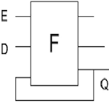
The characteristic equation of the D latch can be written as Q+ = D · E + .E · Q. In the proposed work, enable (E) refers to the clock and is used conversely in place of clock. When the enable signal is 1, the value of the input D is reflected at the output that is Q+ = D. While, when E = 0 the latch preserves its previous state, that is Q+ = Q. In Fig. 1 Reversible D
[image:3.595.69.258.114.197.2]latch is shown and its characteristic equation is reverse of D latch characteristic equation but that design cannot be tested only by two vectors because of feedback. Some misinterruptions may occur.
Fig 1. Reversible D latch
[image:3.595.382.492.176.283.2]So in our proposed work we will cascade two Fredkin gate and Q output of one gate will follow the other. And it has two control signals C1 and C2 by which the design works. In normal mode which is shown in Fig. 2 works when C1 and C2 is given as 0 and 1 and the circuit works as a D latch without any fan-out problem. In test mode which is shown in Fig. 3 and 4 works when C1 and C2 is given as 1 and 1 or 0 and 0, the circuit disrupts the feedback and checks for stuck-at-0 or stuck-at-1 fault.
Fig 2. Normal mode
© 2016, IRJET | Impact Factor value: 4.45 | ISO 9001:2008 Certified Journal | Page 1876 Fig 4. Test mode for stuck-at-1 fault
B. DESIGN OF TESTABLE NEGATIVE ENABLE D LATCH
A negative enable reversible D latch will pass the input D to the output Q when E = 0; otherwise preserves the previous state. The characteristic equation of the negative enable D latch is Q+ = D·E
+E·Q. This characteristic equation of the negative enable reversible D latch can be mapped on the second output of the Fredkin gate. The next Fredkin gate in the design take cares of the FO. This Fredkin gate in the design also helps in making the design testable by two test vectors, all 0’s and all 1’s, by breaking the feedback based on control signals C1 and C2 as illustrated above for positive enable D latch. The negative enable D latch is helpful in the design of testable reversible master-slave flip flops. This is because as it can work as a slave latch in the testable reversible master-slave flip-flops in which no clock inversion is required.
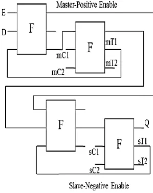
C. DESIGN OF TESTABLE MASTER-SLAVE FLIPFLOPS
We have proposed the design of testable flip-flops using the master slave strategy that can be tested for any stuck-at faults using only two test vectors, all 0s and all 1s. Master latch will be positive enabled Fredkin gate based D latch and slave latch will be negative enabled Fredkin gate based D latch. Fig 5 shows the master-slave D flip flop. There are 4 control signals sC1, sc2, mC1 and mc2. mC1 and mC2 control the master latch and similarly sC1 and sC2 control the slave latch. When signals are given as 0 and 1 it will work in normal mode and avoid fan out problem. If the signals are given 0 and 0 it will disrupt the feedback and test the circuit for stuck-at-1 fault. Suppose if the signals are given as 1 and 1 then it will test the circuit for stuck-at-0 fault. Here Master controls the slave latch. If signal is given as 1 master latch works and vice-versa slave latch will work.
Fig 5. Master-slave D flip-flop
D. DESIGN OF TESTABLE REVERSIBLE DET FLIP FLOPS
In the master-slave flip-flop, it does not sample the data at both clock edges; instead it waits for the next rising edge of the clock to work as a master or slave latch. In order to overcome the abovementioned problem, researchers have introduced the concept of DET flip-flops which sample the data at both the edges. Thus, DET flip-flops can sample and receive two data values in a clock period thus frequency of the clock can be reduced to half of the master- slave flip-flop while maintaining the same data rate. The half frequency operations make the DET flip flops very much useful for low power computing as frequency is equal to power consumption in a circuit. It is designed by connecting the two latches, via, the positive enable and the negative enable in parallel rather than in series. The 2:1 Multiplexer at the output transfer the output from one of these latches which is in the storage state .
[image:4.595.75.245.100.212.2]© 2016, IRJET | Impact Factor value: 4.45 | ISO 9001:2008 Certified Journal | Page 1877 the controls signals of the testable negative enable
[image:5.595.340.556.101.252.2]D latch, while pC1 and pC2 are the control signals of the testable positive enable D latch. Depending on the values of the pC1, pC2, nC1, and nC2, the testable DET flip-flops work either in normal mode or in the testing mode. In normal mode pC1 and pC2 are given as 0 and 1 and similarly nC1 and nC2 are given as 0 and 1. The pC1 = 0, pC2 = 1 help in copying the output of the positive enable D latch thus avoiding the Fan-out while the nC1 = 0 and nC2 = 1 help in copying the output of the negative enable D latch thus avoiding the FO. Similarly in test mode if all signals are given as 0 then it tests the circuit for stuck-at-1 fault. If all the signals are given as 1 then it tests for stuck-at-0 fault.
Fig 6. DET flip-flop
[image:5.595.336.538.295.451.2]Fig 7. Normal mode
Fig 8. Test mode for stuck-at-1 fault
Fig 9. Test mode for stuck-at-0 fault
IV. RESULT AND DISCUSSION
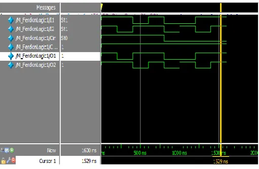
[image:5.595.60.261.299.680.2]In this section all the simulation results which are done using Xilinx ISE simulator are shown Fig
Fig.10 Fredkin gate
[image:5.595.317.573.542.709.2]© 2016, IRJET | Impact Factor value: 4.45 | ISO 9001:2008 Certified Journal | Page 1878 the control signal is given as 0 then the 2 outputs
obtained is the swapping of inputs.
Fredkin Based Reversible Master Slave DFF:
Fig.11. Simulation of Fredkin Based Reversible Master Slave DFF
V. CONCLUSION AND FUTURE SCOPE
This paper proposed reversible sequential circuits based on conservative logic that is testable for any unidirectional stuck-at faults using only two test vectors, all 0s and all 1s. The proposed sequential circuits based on conservative logic gates outperform the sequential circuit implemented in classical gates in terms of testability. The sequential circuits implemented using conventional classic gates do not provide inherited support for testability. Hence, a conventional sequential circuit needs modification in the original circuitry to provide the testing capability. Also as the complexity of a sequential circuit increases the number of test vector required to test the sequential circuit also increases. For example, to test a complex sequential circuit thousand of test vectors are required to test all stuck-atfaults, while if the same sequential circuit is build using proposed reversible sequential building blocks it can be tested by only two test vectors, all 0s and all 1s.
REFERENCES
[1] Prasanna.M and Amudha.S “Implementation of Testable reversible sequential circuit of FPGA” IEEE Sponsored 2nd International Conference on
Innovations in Information Embedded and Communication system ICIIECS,2015.
[2] J. Ren and V. K. Semenov, ‘‘Progress with physically and logically reversible superconducting digital circuits,’’ IEEE Trans. Appl. Superconduct.,vol. 21, no. 3, pp. 780--786, Jun. 2011.
[3] S. F. Murphy, M. Ottavi, M. Frank, and E. DeBenedictis, ‘‘On the design of reversible QDCA systems,’’ Sandia National Laboratories, Albuquerque, NM, Tech. Rep. SAND2006-5990, 2006.
[4] H. Thapliyal and N. Ranganathan, ‘‘Reversible logic-based concurrently testable latches for molecular QCA,’’ IEEE Trans. Nanotechnol., vol. 9, no. 1, pp. 62--69, Jan. 2010.
[5] P. Tougaw and C. Lent, ‘‘Dynamic behavior of quantum cellular automata,’’ J. Appl. Phys., vol. 80, no. 8, pp. 4722--4736, Oct. 1996.
[6] M. B. Tahoori, J. Huang, M. Momenzadeh, and F. Lombardi, ‘‘Testing of quantum cellular automata,’’ IEEE Trans. Nanotechnol., vol. 3, no. 4, pp. 432--442, Dec. 2004.
[7] G. Swaminathan, J. Aylor, and B. Johnson, ‘‘Concurrent testing of VLSI circuits using conservative logic,’’ in Proc. Int. Conf. Comput. Design, Cambridge, MA, Sep. 1990, pp. 60--65.
[8] E. Fredkin and T. Toffoli, ‘‘Conservative logic,’’ Int. J. Theor. Phys., vol. 21, nos. 3--4, pp. 219--253, 1982.