ISSN(Online): 2320-9801
ISSN (Print): 2320-9798
I
nternational
J
ournal of
I
nnovative
R
esearch in
C
omputer
and
C
ommunication
E
ngineering
(An ISO 3297: 2007 Certified Organization)
Vol. 3, Issue 12, December 2015
Design and Implementation of an Efficient
Router for 3D Network-On- Chip
Shrushti Tapar, Jinal Tapar, Aashish Kharate
M.E student, Dept of EXTC, SGBA University, Maharashtra, India
M.E student, Dept of EXTC, SGBA University, Maharashtra, India
Assistant Professor, Dept. of EXTC, SGBA University, Maharashtra, India
ABSTRACT: - The present chip manufacturing trend is moving towards ultra large scale integration, making it possible to accommodate complete assembly of modules/processing element on a single chip i.e. the concept of system on chip(SoC) has emerged. Conventional bus-based systems are no longer reliable architecture for SoC due to a lack of scalability and parallelism integration, high latency and power dissipation, and low throughput. Network-on-Chip (NoC) has been discovered as a promising solution for future systems on chip design and is in its state-of-art. It offers more scalability than the shared-bus based interconnection, allows more processors to operate concurrently. Recently, due to advancements in the 3D integration of chips using through silicon via (TSV), merging NoC to the third dimension (3D-Noc) has been proposed to deal with the problems encountered in 2D NoC. This offers solution of lower power consumption and higher speed. Thus, a 2x2x4 mesh topology virtual channel router is being designed, simulated and synthesized in Xilinx ISE design suite.
KEYWORDS: SoC, NoC, TSV, router, virtual channel, 3D
I. INTRODUCTION
In this era of digital technology, the core of each electronic system, from a phone to a satellite communication system, from a television to a spacecraft etc., is a System on Chip (SoC). A SoC is a complete assembly of various PE (processing elements), memories and other peripherals incorporated on-chip, for accomplishing a specific application in a small area. Global interconnects like the shared buses system are becoming the principal performance bottleneck for high performance Systems-on-Chip (SoCs) [1], [2]. The main purpose for the SoC system is to shrink the size of the chip as smaller as possible while ensuring at the same time for more scalability, higher bandwidth and lower latency. Thus, conventional bus-based-systems are no longer reliable architecture for SoC due to a lack of scalability and parallelism integration, high latency and power dissipation, and low throughput. The network-on-chip (NoC) architectures have been proposed to replace the conventional global interconnections that will have severe problems because of the scalability and high-bandwidth requirement of the multi-/many-core chips [3, 4].
Network-on-Chip [1], [3] has been discovered as a path-breaking method that can overcome these problems by employing a simple and scalable architecture platform, inspired by the Internet. NoC serves as a medium to interconnect processors, memories and other custom designs together using switching packets rather than switching messages or words, which makes NoC an attractive option to provide a higher bandwidth and higher performance. On the other hand, it is inevitable fact that as future applications get more complicated, the need for a high performance system that handles increase complexity will incorporate thousands of cores on a single chip. For these ultra high performance applications, such us real-time radio telescope signal processing, image/video processing, a good architecture has to be designed to ensure a sufficient bandwidth for any collaboration between memories and cores as well as between different cores on the same chip. Thus, the concept of network-on-chip (NoC) stands as a best candidate for all of the mentioned needs.
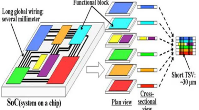
Figure 1: Concept of SoC and 3D structure with through silicon via (TSV)
The advantages of 3D structure such as multi-layered which has provided with increased number of PE to incorporate on a chip and at the same time due to through silicon via (TSV) that is interconnection of silicon between two consecutive layers which has tremendous enhanced the inter-layered communication speed.
Thus, accumulating all the discussion so far, this paper aims at combining the NoC structure with the benefits of the 3D integration to present 3D-NoC as a new architecture. This architecture responds to the scaling demands for future SoC, exploiting the short vertical links between the adjacent layers that can clearly enhance the system performance. So, amalgamation of above two techniques leads to 3D NoC for better performance of SoCs. 3D technology bridges the processor-memory performance gap: Unlike a conventional 2D chip, on which logic and memory units reside at opposite ends, a 3D chip can have logic and memory stacked together to shorten the critical path. More importantly, bringing main memory onto the chip can significantly reduce latency.
II. RELATED WORK
The advantages of 3D NoC have been already discussed earlier. Due to the need of increasing scalability in structure and ultra high speed for applications such as real time video processing, continuously research is going on since long in this area and one of the solutions is proposed here. Starting chronologically with the work that has contributed its part of research and forming base for this paper.
Firstly, a survey report on NoC by Shankar et al [12] had pointed out that the scaling of microchip technologies has enabled large scale systems-on-chip (SoC). They manifested out that Network-on-chip (NoC) research addresses global communication in SoC, involving (i) a move from computation-centric to communication-centric design and (ii) the implementation of scalable communication structures. The survey, represents that a perspective on existing NoC research. In the paper [10], it was presented by William J. Dally that the network efficiency can be enhanced by dividing buffer storage associated with each channel into numerous small channels which are called as “virtual channels”. Also, the abstractions such as system, network adapter, network, and link to explain and structure the fundamental concepts, actual network design, system level design and modeling has been discussed. Related to the 3D integration technology, Topol et al in [7] stated, 3D-IC can improve the performance even in absence of scalability. They showed that aside from this clear benefit, package density is increased significantly, power is reduced from use of shorter wires, and circuitry is more immune to noise [5]. According to Feero et al [8], 3D-NoC has the ability to decrease the number of hops, a basic and important factor to evaluate the system performance.
ISSN(Online): 2320-9801
ISSN (Print): 2320-9798
I
nternational
J
ournal of
I
nnovative
R
esearch in
C
omputer
and
C
ommunication
E
ngineering
(An ISO 3297: 2007 Certified Organization)
Vol. 3, Issue 12, December 2015
design using Wormhole switching and Stall-and-Go flow control scheme. Although NoC has its advantages over the shared-bus based systems, it has also some limitations such as high power consumption, high cost communication, and low throughput. To overcome those limitations, the other proposed system is a 3D-NoC which is an extension of 2D NoC.In this we are taking forward the 3D NoC work by designing 2x2x4 NoC with mesh topology virtual channel and stall and go flow control scheme with our Look ahead XYZ routing algorithm.
III.3DNOCARCHITECTURE
Combining the NoC structure with the benefits of the 3D integration leads us to present 3D-NoC as a new architecture. The details of this architecture are presented in this section below:
A. Topology
Basically, topology is defined as the pattern or fashion of arranging various modules in the system.
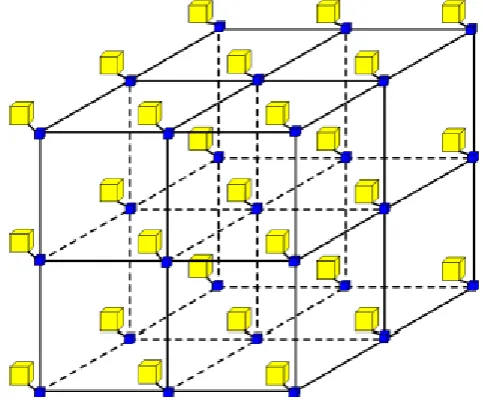
3D NoC, as illustrated in Fig.2, is a simple 3x3x3 mesh topology. Every –node have three co-ordinates namely X, Y and Z. Here we have chosen mesh topology because of its some advantageous features such as simple configuration, low complexity and concurrent data transmission.
Figure 2: 3D-NoC 3x3x3 mesh topology
B. Router
Figure 3: Router pipeline stages of 3D NoC
1) Buffer Writing (BW):
The input buffer simply stores incoming flits before it moves further toward computing routing algorithm. The depth of input buffer is equal to four and each of four can store flit size up to 81 bits as shown in figure. The arbitration is done by using FIFO scheme to manage flits. The buffer occupies sufficiently large amount of area of router but nevertheless improves the performance of system.
ISSN(Online): 2320-9801
ISSN (Print): 2320-9798
I
nternational
J
ournal of
I
nnovative
R
esearch in
C
omputer
and
C
ommunication
E
ngineering
(An ISO 3297: 2007 Certified Organization)
Vol. 3, Issue 12, December 2015
C. Routing Calculation (RC):
At each input port when flit comes its destination address is fetch and decoded destination address is compared with present node address and comparative computation are done to proceed the flit to particular direction to next node. The computations are done as below
if xdest is larger than xaddr then New-Next-Port will be EAST. In the opposite case New-Next-Port will be WEST.
if ydest is larger than yaddr then New-Next-Port will be NORTH, else New-Next-Port will be SOUTH.
if zdest is larger than zaddr then Port will be UP, and if this condition is not satisfied New-Next-Port will be DOWN.
if xdest is equal to xaddr, ydest is equal to yaddr and zdest is equal to zaddr then New-Next-Port will be SELF.
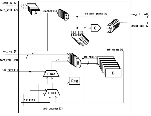
D. Switch Allocation (Sw):
After the routing calculation stage, the information about the New-Next-Port is transmitted to the switch allocator as shown in Fig.5. The main function of the switch allocator is to decide which output port should be granted to which input port, and when this grant should be allocated. When several flits compete for the same output port, 3D NoC arbiter in the switch allocator schedules a round-robin scheme. This scheme allows for each request to be served in a fair way, without taking into consideration priority.
Figure 5: Switch allocator circuit
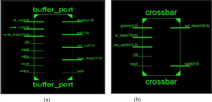
D. Crossbar traversal (CT):
Figure 6: Crossbar circuit
E. Flit Structure
3D NoC adopts wormhole switching. Each flit is 81 bits where the first bit indicates the tail and the next seven bits are dedicated to indicate the Next-Port direction. Then three bits are used to store destination information about each (xdest, ydest and zdest). Data can be found in the remaining 64 bits. Figure.7 shows more details about the 3D NoC flit format.
Figure 7: 3D NOC flit format:
IV.HARDWARE EVALUATION
The router for 3D NoC is designed in Verilog HDL using Xilinx‟s ISE design suite EDA tool. The synthesis results shown below of each of the modules of router is shown in figure 8. It gives us the detail of actual implementation of the designed modules in terms of the basic combinatorial and sequential circuits.
ISSN(Online): 2320-9801
ISSN (Print): 2320-9798
I
nternational
J
ournal of
I
nnovative
R
esearch in
C
omputer
and
C
ommunication
E
ngineering
(An ISO 3297: 2007 Certified Organization)
Vol. 3, Issue 12, December 2015
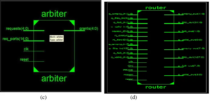
(c) (d)
Figure 8: (a) RTL Schematics for Input buffer with the flit depth of four (b) Schematic for Crossbar (c) RTL schematic for Arbiter (d) RTL schematic for router of 3D NoC
After the HDL synthesis phase of the synthesis process, the RTL Viewer is used to view a schematic representation of the pre-optimized design in terms of generic symbols that are independent of the targeted Xilinx device, for example, in terms of adders, multipliers, counters, AND gates, and OR gates.
Figure 8(d) the top block automatically generated by RTL Viewer when router.ngr file is opened and run. Further opening means elaborating this top block gives all the basic components utilized and their inter-connections in detail to realize the proposed designed system can be visualized and analyzed from figure
Table 1: Utilization summary
Estimated Values Numbe r of slice LUTs Number of fully used LUT-FF pairs Number of bonded IOBs Number of BUFG/BUFGC TRls Input arbiter
Used 199 4 27 1
Available 69120 203 640 32
Utilization 0% 1% 4% 3%
Buffer Used 519 197 77 1
Available 69120 928 640 32
Utilization 0% 21% 12% 3%
Crossbar Used 384 0 347 1
Available 69120 384 640 32
Utilization 0% 0% 54% 3%
Router Used 11612 2204 379 1
Available 46560 12050 240 104
Utilization 24% 18% 157% 0%
V. CONCLUSION AND FUTURE WORK
The most crucial element in the network which manages the communication traffic between various processing elements is a router. The various components of a router such as input arbiter, input buffer, switch allocator, crossbar and mainly routing algorithm has been designed successfully.
For the future work we will to implement the network interface (NI) connecting router and other PE/ dummy nodes (SRAM) to form complete system. We will also try to run some mathematical application
REFERENCES
1. Pande P.P., Grecu C., Jones M., Ivanov A., Saleh R.: „Performance evaluation and design trade-offs for network-on-chip interconnect
architectures‟, IEEE Trans. Comput., 2005, 54, (8), pp. 1025–1040
2. Vangal S., Howard J., Ruhl G., ET AL.: „An 80-tile 1.28tflops network-on-chip in 65 nm cmos‟. Proc. IEEE Int. Solid-State Circuits Conf.,
February 2007, pp. 98–589
3. Bell S., Edwards B., Amann J., ET AL.: „Tile64 processor: a 64-core soc with mesh interconnect‟. Proc. IEEE Int. Solid-State Circuits Conf.,
February 2008, pp. 88–598
4. Bahn J.H., Lee S.E., Bagherzadeh N.: „On design and analysis of a feasible network-on-chip (noc) architecture‟. Proc. Fourth Int. Conf. Information Technology, April 2007, pp. 1033–1038
5. G. Philip, B. Christopher, and P. Ramm, Handbook of 3D Integration: Technology and Applications of 3D Integrated Circuits, Wiley-VCH,
2008.
6. L. P. Carloni, P. Pande, and Y. Xie, Networks-on-chip in emerging interconnect paradigms: Advantages and challenges, In Proceedings of the
3rd ACM/IEEE International Symposium on Networks-on-Chip (NOCS09), San Diego, CA, May 2009, pp. 93-102.
7. W. Topol, J. D. C. La Tulipe, L. Shi, D. J. Frank, K. Bernstein, S. E. Steen, A. Kumar, G. U. Singco, A. M. Young, K. W. Guarini, and M.
Ieong, Three-dimensional integrated circuits, IBM Journal of Research and Development, vol. 50, no. 4/5, pp. 491506, July 2006.
8. B. Feero, P. Pratim Pande, Performance Evaluation for Three-Dimensional Networks-on-Chip, Proceedings of IEEE Computer Society Annual
Symposium on VLSI (ISVLSI), 9th-11th May 2007, pp. 305-310.
9. William J. Dally, member IEEE, “Virtual channel flow control”, IEEE transaction on Parallel and Distributed systems, VOL. 3 NO. 2, March
1992
10. Christianto C. Liu, Ilya Ganusov, Martin Burtscher, and Sandip Tiwari, Cornell University, “Bridging the Processor-Memory Performance Gap
with 3D IC Technology” ,Co-published by the IEEE CS and the IEEE CASS IEEE Design & Test of Computers 2005 IEEE
11. Tobias Bjerregaard and Shankar Mahadevan, Technical University of Denmark, “A Survey of Research and Practices of Network-on-Chip”,
ACM Computing Surveys, Vol. 38, March 2006, Article 1.
12. K. Mori, A. Ben Abdallah, K. Kuroda, Design and Evaluation of a Complexity Effective Network-on-Chip Architecture on FPGA, Proc. of The