Implementation of a Multi-channel UART
Controller Based on FIFO Technique using Spartan3AN FPGA
Shivarudraiah. B
1, Suryakanth. B. M
2Assistant Professors, Department of Electronics and Communication Engineering1, 2 BMS Institute of Technology, Bangalore-560056
Affiliated to Visveswaraiah Technological University, Belgaum-590014, INDIA
[email protected] [email protected]
Abstract: In order to meet the complex control systems communication demands, the paper presents a multi-channel UART controller based on FIFO(First In First Out) technique and FPGA(Field Programmable Gate Array). The paper presents design method of asynchronous FIFO and structure of the controller. This controller is designed with FIFO circuit block and UART (Universal Asynchronous Receiver Transmitter) circuit block within FPGA to establish communication in complex control systems quickly and effectively. From the simulation results, it is easily to know that this controller can be used to implement communication when master equipment and slaver equipment are set at different Baud Rate. It can also be used to reduce synchronization error between sub-systems in a system with several
sub-systems. The controller is reconfigurable and scalable.
Keywords: FIFO, FPGA, UART, BAUD RATE
I INTRODUCTION
Today, owing to availability of state-of-the-art microcontrollers and digital signal processors (DSPs), complex control algorithms can be easily implemented to attain the desired system performance. But in actual control systems, it is difficult to attain the expected result for various factors affecting the control systems such as control algorithms itself, capability of controllers and states of control circumstance [1]. Except these factors, communication parameters of control systems including Baud Rate, BER (Bit Error Rate) and synchronization between sub-systems also engender great effect. In order to improve precision of control system and make good use of modern control algorithms, we should pay much more attention on communication in control systems.
In most of the control systems, UART a kind of serial communication circuit is used widely. A universal asynchronous receive/transmit (UART) is an integrated circuit which plays the most important role in serial communication. It handles the conversion between serial and parallel data. Serial communication reduces the distortion of a signal, therefore makes data transfer between two systems separated in great distance possible [2].
In some complex systems, communications between the master controller and slave controllers are implemented by serial or parallel port. Parallel communication needs a lot of multi-bit address bus and data bus and it is only convenient for short distance transmission. Serial communication is another way of communication used extensively because of its simple structure and long transmission distance. But sometimes a common serial port could not meet requirements of complex systems with different Baud Rates equipments even some special Baud Rate equipments. As shown in Fig. 1, in a system, the PC’s Baud Rate is 115200bps and the Ep1 i.e. equipment 1’s Baud Rate is 57600bps, equipment 2’s Baud Rate is 19200bps, and other equipments are set at 9600bps or other Baud Rates. It is impossible to implement this multi-Baud Rate communication system without a special Baud Rate converter.
As a second example consider a 6-DOF robot, where in there are 6 sub-controllers which are all the same structure to be designed. The PC is used to implement the control algorithm of the robot and send control parameters to sub-controllers and sub-controllers are used to collect feedback signals and send them to the PC. The PC and sub-controllers communicate with each other on a RS485 BUS NET. Each sub-controller has a unique address number and the PC uses this number to identify each sub-controller. When the PC wants to send data to node 6, it has to access front 5 nodes, this engenders time delay and makes performance of the robot’s each DOF not synchronized.
So it reduces the control algorithm’s precision and brings difficulties in researching of the control algorithm. To solve these problems described as above, we design a multi-channel UART controller based on FIFO technique and implementing it on FPGA. It can receive data with a UART block at a certain Baud Rate and transmit data to sub-equipment with a UART block at the same Baud Rate or at other kind of Baud Rate which is different from the receiving Baud Rate.
FIFO is the most important part of these systems and it works as a bridge between different devices [3][4]. As the same, in our controller, asynchronous FIFO based on FPGA is also the most important part. So the features and capabilities of the asynchronous FIFO determine the features of our controller.
II DESIGN OF ASYNCHRONOUS FIFO’S
A Introduction to FIFO
An asynchronous FIFO refers to a FIFO design where data values are written to a FIFO buffer from one clock domain and the data value are read from the same FIFO buffer from another clock domain, where the two clock domains are asynchronous to each other. FIFOs are always used for data cache, storing differences of frequency or phase of asynchronous signals. And asynchronous FIFOs are often used to quickly and safely pass data from one clock domain to another asynchronous clock domain. In asynchronous clock circuit, periods and phases of each clock domain are completely independent so the probability of data loss is always not zero. This paper introduces a way of designing FIFO based on FPGAs with high write/read speed and high reliability.
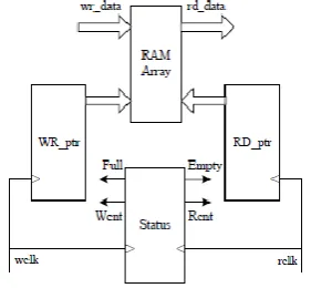
Fig. 2: Asynchronous FIFO structure diagram
Generally, a FIFO consists of a RAM Array block, a Status block, a write pointer (WR_ptr) and a read point (RD_ptr) and its structure is shown in Fig. 2. A RAM array with separate read and write ports is used to stored data. The write pointer points to the location that will be written next, and the read pointer points to the location that will be read currently. A write operation increments the write pointer and a read operation increments the read pointer. On reset, both pointers are reset to zero, the FIFO is empty. The write pointer happens to be the next FIFO location to be written and the reader pointer is pointing to invalid data. The responsibility of the status block is to generate the “Empty” and “Full” signals to the FIFO. If the “Full” is active then the FIFO can not accommodate more data and if the “Empty” is active then the FIFO can not provide more data to readout. When writing data into the FIFO “wclk” will be used as the clock domain and when reading data out of the FIFO “rclk” will be used as the clock domain. These both clock domains are asynchronous.
B Status of Empty and Full of FIFO
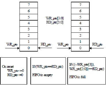
Creating empty and full signals is the most important part of designing a FIFO. No matter under what circumstance, the read and write pointers can not point to the same address of the FIFO. So, the empty and full signals play very important roles within FIFO that they block access to further read or write respectively. If a reset or read makes the pointers equal to each other, the FIFO is really empty. If a write makes the pointers equal, the FIFO is full [4].
In order to exactly know whether the FIFO is full or empty, we can set a direction flag keeps track of what causes the pointers to become equal to each other. The flag tells the status circuit the direction in which the FIFO is currently headed. The implementation of the direction flag is a little complex because you have to set the threshold of “going toward full” and “going toward empty”. In this paper, this method is instead of another design technique used to distinguish between full and empty is to add an extra bit to each pointer. The pointers length n equals to log2 (array _ size) .The array _ size is the depth of the FIFO needed in a project. For example, when setting the array _ size of the FIFO 64 byte (8 bits one byte), the writer and read pointers’ length is 2 log 64 = 6 . Using n +1 bits pointer when n is the number of address bits required to access the entire FIFO memory buffer. When both pointers including the MSBs are equal the FIFO is empty. And the FIFO is full when both pointers, except the MSBs are equal. As Fig. 3 shows, when the array _ size of the FIFO is 8 bytes, the number of address bits required to access the entire FIFO memory buffer is 4. With an additional address bit the full and empty signals can be easily created [4].
The status block fundamentally performs operations on the two pointers, and these run off two different clock domains. This is what causes the real difficulty. If you were to sample the read pointer with the write pointer (or vice versa), you will potentially run into a problem called metastability. Metastability is the name for the physical phenomenon that happens when an event tries to sample another event. In a physical circuit the metastability causes the output uncertainty either be a logical 1 or a logical 0 or something between.
Fig. 3: FIFO full and empty conditions
III IMPLEMENTATION OF A MULTI-CHANNEL UART CONTROLLER
A Hardware structure
In the multi-channel controller, there are different blocks including UART block, Status Detectors, asynchronous FIFOs block and Baud Rate Generator block. Each block has different function in the controller. The first part is UART circuit block and its structure is shown in Fig. 4. It consists of three parts Receive Circuit, Transmit Circuit and Control/Status Registers. The Transmit Circuit consists of a Transmit Buffer and a Shift Register. Transmit Buffer loads data being transmitted from local CPU. And Shift Register accepts data from the Transmit Buffer and send it to the TXD pin one by one bit.
Fig. 4: Structure of UART block
Using FIFO technique and the COM block as mentioned before, we design a multi-channel controller. Structure of the controller is showing in Fig. 5.
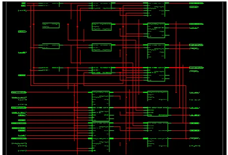
Fig. 5: Structure of a multi-channel UART controller
B Software structure
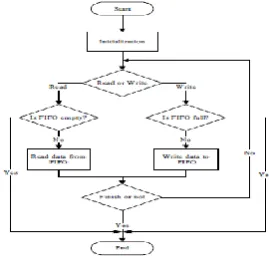
Software coding is done in Verilog HDL to design FPGAs hardware architecture, it is easy to create and adjust to satisfy requirements of applications. One UART is used to communicate with PC with other main MCU and there are also four other UARTs used to communicate with sub MCUs. Each channel has two FIFOs, one for receiving data and the other for transmitting data. The software flow chart is shown in Fig. 6.
Fig. 6: The Software flow chart
IV SIMULATION, VERIFICATION AND SYNTHESIS
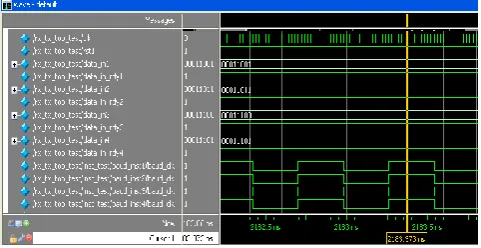
To verify design of the controller a test bench is written to make verification in Modelsim XE 6.4b simulation tool. Also the design is synthesized and tested using Xilinx ISE 10.1 and implemented on Spartan3AN FPGA board. Data received from the PC or other main MCU will be stored in FIFOs within FPGA till the controller received the commands to order the controller to send data to sub-controllers. When sub-controllers are required to receive data at different Baud Rates, the controller can set each channel at its required Baud Rate to transmit data. All sub-MCU can receive data at the same time.Then the controller will set a kind of Baud Rate according to commands desired. As shown in Fig. 7, the controller is receiving data and store the data received to different FIFO waiting for read. The transmitting sequence is showing as following in Fig. 8. The controller sends data at the same time but at different Baud Rate.
Four channels are designed using Verilog HDL as totally the same structure which makes use of always block to implement communication.So there are no time differences between sub-controller when the main controller transmits data to sub-controllers at the same time.So using this controller can greatly improve synchronization of sub-controllers.
Fig. 7: Baud clock generation for Baud rate of 119200 Hz
Fig. 8: Baud clock generation for Baud rate of 9600 Hz
Fig. 10: Transmitting sequence at different baud rate
Fig. 11: Transmitting and receiving data from same UARTs
Fig. 12: Transmitting and receiving data from different UARTs
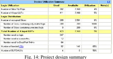
Fig. 14: Project design summary
V CONCLUSION
Multi channel UART controller introduces a method to design asynchronous FIFO based on FPGA. The controller can be used to implement communication in complex systems with different Baud Rates of sub-controllers. It also can be used to reduce time delays between controllers of a complex control system to improve the synchronization of each sub-controller. The controller’s fault is that it would be influenced by the radiation from surroundings and by short-time pulses.
VI ACKNOWLEDGMENT
This work is carried out under the guidance of “L. Akalpitha Kulkarni, Associate Professor, Department of Electronics and Communication Engineering, Dr Ambedkar Institute of Technology”, Bangalore-560056, INDIA.
REFERENCES
[1] B. Zeidman, “Designing with FPGAs & CPLDs”, CMP Books, 2002
[2] C. E. Cummings, “Simulation and Synthesis Techniques for Asynchronous FIFO Design”, SNUG San Jose 2002.
[3] L. K. Hu and Q.CH. Wang, “UART-based Reliable Communication and performance Analysis”, Computer Engineering, Vol 32 No. 10, May 2006.
[4] S. E. Lyshevski, “Control Systems Theory with Engineering Applications”, Birkhauser Boston, 2001.
[6] X. D. Wu and B. Dai, “Design of Interface between High Speed A/D and DSP Based on FIFO”, Journal of Beijing Institute of Petrochemical Technology Vol. 14 No.12, June 2006, pp26-29
[7] Samir Palnitkar, “Verilog HDL: A guide to digital design and synthesis”, Vol. 1, Second Edition, 2003
BIOGRAPHY
Shivarudraiah .B obtained M.Tech degree in Dr. Ambedkar Institute of Technology in year 2010. Started teaching carrier as Lecturer in Basava Academy of Engineering. Currently working as Assistant Professor in BMS Institute of Technology. Research areas include VLSI design, Image processing and Embedded
systems.
Suryakanth. B. M obtained M.Tech degree in Dayanand Sagar College of Engineering in year 2008. Started teaching carrier as Lecturer in KNSIT. Currently working as Assistant Professor in BMS Institute of Technology.