A New Proposal for 4-to-2 Optical Encoder Using
Nonlinear Photonic Crystal Ring Resonators
Fatemeh Hadadan and Mohammad Soroosh*
Department of Electrical Engineering, Shahid Chamran University of Ahvaz, Ahvaz, Iran *Corresponding Author's Email: [email protected]
Received: Jan. 22, 2018, Revised: May. 29, 2018, Accepted: Aug. 15, 2018, Available Online: Dec. 27, 2019 DOI: 10.29252/ijop.13.2.119
ABSTRACT— In this paper, we proposed an all
optical 4-to-2 encoder that has 4 input and 3 output ports. This device generates a 2 bit binary code based on which input port is active. We used nonlinear photonic crystal ring resonators along with optical power splitter for realizing the proposed encoder. In this device the switching rate and area are obtained about 333 GHz and 612µm2 respectively.
KEYWORDS: Kerr effect, Optical encoder,
Photonic bandgap, Photonic crystal.
I.
I
NTRODUCTIONOptical logic devices are important building blocks that can be used in all optical networking and optical signal processing. High speed and high band width are the major benefits of optical networks and optical signal processing [1]. In order to avoid undesirable delays imposed by conversion from electrical to optical and optical to electrical in optical networks, we need all optical networks in which all process is done in optical form [2]. The main prerequisite for realizing all optical networks is to have all optical devices. Optical logic devices such as optical logic gates, decoders, multiplexers and encoders are the fundamental elements in optical logic circuits used for optical signal processing.
Optical encoder is a logic device that has 2N input and N output ports. Optical encoder generates an N bit code based on which input port is active. Beside their applications in optical signal processing systems, optical encoders are one the main building blocks in all optical analog to digital converters (ADCs). In realizing optical ADCs after creating
discrete levels of input analog signal, we need an optical encoder to convert the discretized levels of input analog signal into standard binary codes [3-5].
Photonic crystals (PhCs) can be used for designing all optical devices. Periodic distribution of refractive index in these structures results in photonic band gap (PBG), with which they can control and confine the propagation of optical waves inside very compact dimensions [6]. PhC based devices are scalable and very flexible. Therefore, by changing lattice constant or other structural parameters of the structure it is possible to easily control the optical behavior of the device [7-9].
Due to these properties, it has been shown that PhCs are suitable for designing many optical devices such as optical filters [10-14], demultiplexers [15-17], switches [18-20], logic gates [21-24], and decoders [25-27].
Moniem [28] proposed an all optical 4-to-2 digital encoder, in which he combined 4 resonant rings with T-waveguide to design the proposed encoder. The switching speed and area of this encoder are 500 GHz and 1225 µm2 respectively. By combining elliptical ring resonators and PhC waveguides, Hassangholizadeh-Kashtiban et al. proposed an all optical 4 to 2 reversible encoder [29]. The area of this structure is 217 µm2. Alipour-banaei et al. [30] proposed another optical encoder by combining self-collimation effect of PhC structures with power splitters and reflectors, in which the lattice constant is 1 µm, which results in a large area (3795 µm2).
Also its performance is very sensitive upon the phase of input light. They reported response time as long as 1.4 ps for their presented structure.
In this paper, we aim to design a compact all optical 4-to-2 optical encoder whose area and switching speed are suitable for employing in optical integrated circuits (OICs). For this purpose, we will combine nonlinear Kerr effect with PhC ring resonator structure. We used plane wave expansion (PWE) and finite difference time domain (FDTD) methods [31, 32] for analyzing and simulating the proposed structure and obtaining its optical behavior.
The rest of the paper is organized as follows: in section 2 we will propose the basic photonic crystal ring resonator based switch structure used for designing the encoder, in section 3 we are going to discuss the design procedure and simulation results of the optical encoder and finally in section 4 we will conclude from our work.
II.
F
UNDAMENTALS
WITCHFor realizing the proposed 4-to-2 optical encoder we need to design a fundamental switch. The basic PhC platform used for designing the optical switch is a 29×23 array of silicon rods with square lattice in the z and x directions. The rods are oriented along the y-axis. The refractive index and radius of the dielectric rods are n=3.46 and r=0.2*a respectively, where a=600 nm is the lattice constant of the structure.
Figure 1 shows that this structure has three PBG regions and we choose the one with the largest width, which is at 0.28<a/λ<0.41 in
TM mode which are equal to 1463nm<λ<2142 nm. In this mode, z-component of the magnetic field is zero. Blue and red colors indicate TM and TE modes in band structure respectively.
The fundamental switch is composed of two parallel optical waveguides and a nonlinear resonant ring which is sandwiched between these waveguides. In the proposed switch, the
upper and lower waveguides are called bus and drop waveguides respectively. As shown in Fig. 2a, the fundamental switch has four ports labelled as A, B, C and D. Port A is the input port and B, C and D are forward transmission, backward drop and forward drop ports. Around the core we put 24 rods made of doped glass, which are shown via green color in Fig. 2(a). The linear refractive index and Kerr coefficient of the doped glass are n0=1.4 and n2=10-14 m2/W [5]. The variation of normalized light intensity at the output ports of the proposed switch is shown in Fig. 2(b).
Fig. 1. The band structure of the fundamental PhC.
Fig. 2. (a) The schematic and (b) the normalized light intensity at output ports of the fundamental switch.
One can see that for lower optical intensities the port B is OFF, and by increasing the input intensity it will turn ON gradually. In this paper the normalized threshold required for the output ports to be considered ON (i.e. Logic 1) is set to be 0.4, also optical intensities less than 0.1 normalized value will be considered OFF (i.e. logic 0). The resonant rings include the nonlinear rods whose refractive indices are depend on the launched optical power in the ring. This issue results in changing power loss for different optical power. So, the difference of the intensity summation in both ends of the device is occurred.
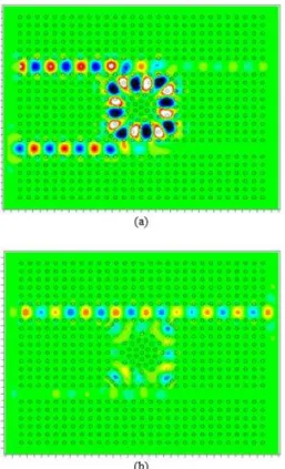
Distribution of optical waves inside the switch for two different optical intensities are shown in Fig. 3. For optical intensity less than 0.2 KW/µm2, most of the optical waves will drop into drop waveguide and travel toward port C, however for optical intensities more than 1.2 KW/µm2 most of the optical waves will travel toward port B.
Fig. 3. Distribution of optical waves inside the structure for (a) Low and (b) High input optical power intensities.
This phenomenon is due to the Kerr effect and refractive index dependency of the PhC
structures optical behavior. When the optical power intensity is low, the central wavelength of the input light coincides with the resonant wavelength of the resonant ring, so the ring will drop light waves into drop waveguide. However, when the optical power intensity reaches to the threshold value, the variation of the refractive index of the dielectric rods, will shift the resonant wavelength of the resonator so that the central wavelength of the input light will not coincide with the resonant wavelength of the resonator. Therefore, the input light will not be dropped into drop waveguide and will travel toward port B.
III.
O
PTICALE
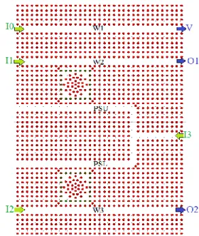
NCODERThe fundamental PhC platform employed for designing the proposed encoder is a 35×50 array of dielectric rods with square lattice. The structural parameters such as refractive index, radius and lattice constant are the same as the proposed switch. So the band structure diagram and PBG region will be the same too. The proposed optical encoder is composed of three optical waveguides – namely W1, W2 and W3 –, two ring resonators – namely R1 and R2 – and an optical power splitter, as shown in Fig. 4. By removing 3 complete rows of dielectric rods the waveguides were created at the appropriate locations inside the fundamental platform. The power splitter is simply created by combining two waveguides with a T-branch structure. The power splitter has two branches – namely upper and lower branch – that are labeled with PSU and PSL respectively.
The first ring resonator (R1) is placed between W2 and PSU and the second ring resonator (R2) is placed between W3 and PSL. The proposed encoder has four input ports and three output ports. The input ports are labeled with I0, I1, I2 and I3. The output ports are labeled with V, O1 and O2. O1 and O2 are the binary output ports and V is used for distinguishing the completely OFF state of the encoder from the state in which I0 is active. The power splitter is designed completely symmetrical so that, it splits the optical
intensity coming from port I3 into 2 identical parts.
After finalizing the design procedure, we are going to simulate the proposed structure and study its optical behavior. For this purpose, we employed optical waves with λ=1550 nm and optical power intensity of P0=0.7 KW/μm2 at each input port. We have to mention that the required threshold for the output ports to be considered ON is 0.4 normalized power. The working states of the encoder are as follows:
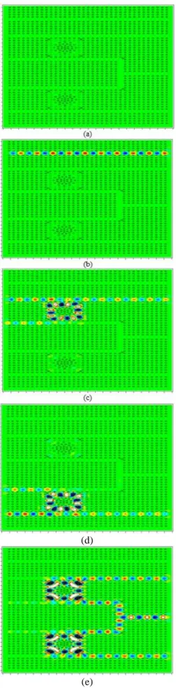
Fig. 4. The final sketch of the proposed encoder. State 1: When all input ports are OFF (i.e. I0=I1=I2=I3=0) which is shown in Fig. 5(a) all the output ports will be OFF, and the encoder generates "00" at the output ports and V=0. State 2: When I0=1and I1=I2=I3=0, which is shown in Fig. 5 (b), the optical power entering the structure from I0 will propagate in W1 and travel toward port V, and will not reach to O1 and O2. So that V will be ON and O1 and O2 will be OFF (i.e. V=1, and O1=O2=0). The normalized power intensity at port V will be about 95%. When I0 is ON the encoder produces "00" binary code at the binary output ports. For both state 1 and state 2, O2O1=00 therefore using port V one can distinguish these states. On the other hands, if no input is applied to the device, port V will be OFF and shows O2O1=00 is due to no input signal and
device is inactive. However, port V will be ON for I0=1 and I1=I2=I3=0 and shows one of the input ports (I0) is active.
State 3: when I1=1 and I0=I2=I3=0, which is shown in Fig. 5(c), the optical waves entering the structure from I1 will propagate inside W2 and travel toward R1. As discussed in section 2 when optical intensity is about 0.7 KW/m2, R1 cannot drop all of the light waves from W2 into PSU, so that the great portion of the light waves will travel toward port O1 but there is no optical power at O2. The normalized light intensity at port O1 and O2 will be about 51% and 1% respectively. Therefore, in this case O1 is ON and O2 is OFF and encoder generates "01" binary code at the output ports. In this case V is OFF.
State 4: when I2=1 and I0=I1=I3=0, which is shown in Fig. 5(d), the optical waves entering the structure from I2 will propagate inside W3 and travel toward R2. As discussed in section 2 when optical intensity is about 0.7 KW/m2, R2 cannot drop all of the light waves from W3 into PSL, so that the great portion of the light waves will travel toward port O2 but there is no optical power at O1. The normalized power intensity at port O1 and O2 will be about 1% and 51% respectively. In this case O1 is OFF and O2 is ON and encoder generates "10" binary code at the output ports. In this case V is OFF.
State 5: when I3=1 and I0=I1=I2=0, the optical signals entering the structure from I3 will be divided into 2 identical parts by the power splitter, one part propagates inside PSU and travel toward R1, and the other part propagates inside PSL and travels toward R2. Therefore, the amount of optical power intensity near each resonator will be about 0.35 KW/m2. So according to Fig. 2(b), R1 and R2 can drop the light waves from PSU and PSL into W2 and W3 respectively, so that light waves will travel toward O1 and O2. The normalized power intensity at both O1 and O2 ports will be about 43%. Therefore, in this case O1 and O2 are ON and encoder generates "11" binary code at the output ports. In this case V is OFF. This is shown in Fig. 5(e).
(d)
(e)
Fig. 5. The working states of the proposed encoder, (a)I0=I1=I2=I3=0, (b) I0=1 and I1=I2=I3=0, (c) I1=1 and I0=I2=I3=0, (d) I2=1 and I0=I1=I3=0, (e) I3=1 and I0=I1=I2=0.
Fig. 6. The time response of the structure for different states (a) I0=1 and I1=I2=I3=0, (b) I1=1 and I0=I2=I3=0, (c) I2=1 and I0=I1=I3=0, (d) I3=1 and I0=I1=I2=0.
Figure 6 shows the time response of the proposed structure, in these diagrams the vertical axis represents the normalized power at the output ports and the horizontal axis shows the “cT” parameter in “μm”, by
dividing the values of the horizontal axis into c=3×10⁸ m/s, one can obtain the time values in second. According to Fig. 6 the delay time for the aforementioned working states are ti=0.05, 3, 3, and 2.5 ps (where i=2, 3, 4, and 5 represents the different working states discussed above).
A shown in Figs. 6(a-c), the normalized power exceeds 1. This issue is due to the resonance phenomenon in both rings. Haus presented a transmission line method based on LC (or second order) circuit for light propagation in cavity and ring resonators [33]. He demonstrated the constructive interferences could be related to the resonance phenomenon. As far as we know the overshoot can be occurred at underdamped case of a second order circuit.
The maximum delay time for the proposed structure is about t=3ps, so that the switching rate of the proposed encoder will be about 333 GHz. These states are summarized in Table 1 and are shown schematically at Fig. 6.
As shown in Table 1 for the proposed structure one can distinguish state 1 (i.e. I0=I1=I2=I3=0) from state 2 (i.e. I0=1 and I1=I2=I3=0). The total area of the proposed structure is about 612μm2.
In order to evaluate the presented device, a comparison between this work and others [28-30] is presented in Table 2. Maximum response time and overall area of the structure are denoted with Tres and Area respectively. One can see the proposed device is more compact than Ref [28, 30]. Although in Ref [30] the low response time is obtained, using self-collimation effect results in more sensitivity rather than the proposed structure in this work. In addition, large area is taking account as an important disadvantage for Ref [30]. Contrast ratio between the normalized power margins for logics 1 and 0 is a significant issue in designing all optical devices. Table 1 demonstrates that this parameter is obtained as large as 0.42 for the proposed device. The calculated value for the mentioned ratio is more than obtained ratio in
Ref [29] (0.35) and is suitable for light coupling from output ports to other devices. With regard to the obtained results, the presented structure can be proposed for using in optical integrated circuits.
Table 1. All working states of the device. Inputs
Outputs Normalized Output Power
Logic Level I0 I1 I2 I3 V O2 O1 V O2 O1 0 0 0 0 0 0 0 0 0 0 1 0 0 0 0.95 0 0 1 0 0 0 1 0 0 0 0.01 0.51 0 0 1 0 0 1 0 0 0.51 0.01 0 1 0 0 0 0 1 0 0.43 0.43 0 1 1 Table 2. Comparison between obtained results in this study and other works.
Reference Tres (ps) Area (μm2)
[28] 2 1225
[29] Not reported 217
[30] 1.4 3795
This work 3 612
IV.
C
ONCLUSIONIn this paper we proposed an all optical 4-to-2 encoder, using 2D PhC structures. The proposed structure was realized by combining optical waveguides, ring resonators and power splitter. The maximum rise time and switching rate were obtained about 3ps and 333 GHz respectively. The overall area of the proposed structure is about 612m2. The proposed structure can generate a 2 bit binary code according to which input port is active.
R
EFERENCES[1] A. Abbasi, M. Noshad, R. Ranjbar, and R. Kheradmand, “Ultra compact and fast All Optical Flip Flop design in photonic crystal platform,” Opti. Commun. Vol. 282, pp. 5073–5078, 2012.
[2] Y. Liu, F. Qin, and Z. Meng, “All-optical logic gates based on two-dimensional low-refractive-index nonlinear photonic crystal slabs,” Opt. Exp. Vol. 19, pp. 1945–1953, 2011.
[3] K. Fasihi, “All-optical analog-to-digital converters based on cascaded 3-dB power splitters in 2D photonic crystals,” Optik- Int. J.
Light Electron. Opt. Vol. 125, pp. 6520–6523, 2014.
[4] B. Miao, C. Chen, A. Sharkway, S. Shi, and D.W. Prather, “Two bit optical analog-to-digital converter based on photonic crystals,” Opt. Exp. Vol. 14, pp. 7966-7971, 2006. [5] B. Youssefi, M.K. Moravvej-Farshi, and N.
Granpayeh, “Two bit all-optical analog-to-digital converter based on nonlinear Kerr effect in 2D photonic crystals,” Opt. Commun. Vol. 285, pp. 3228–3233, 2012.
[6] J. D. Joannopoulos, S.G. Johnson, J.N. Winn, and R. D. Meade, Photonic Crystals: Molding the Flow of Light, Princeton University Press, 2008.
[7] H. Alipour-Banaei and F. Mehdizadeh, “Significant role of photonic crystal resonant cavities in WDM and DWDM communication tunable filters,” Optik- Int. J. Light Electron. Opt. Vol. 124, pp. 2639–2644, 2013.
[8] M. Djavid, F. Monifi, A. Ghaffari, and M.S. Abrishamian, “Heterostructure wavelength division demultiplexers using photonic crystal ring resonators,” Opt. Commun. Vol. 281, pp. 4028–4032, 2008.
[9] F. Mehdizadeh, H. Alipour-Banaei, and S. Seraj-mohammadi, “Channel-drop filter based on a photonic crystal ring resonator,” J. Opt. Vol. 15, pp. 07540, 2013.
[10]H. Alipour-Banaei, M. Hassangholizadeh-Kashtiban, and F. Mehdizadeh, “WDM and DWDM optical filter based on 2D photonic crystal Thue–Morse structure,” Optik- Int. J. Light Electron. Opt. Vol. 124, pp. 4416–4420, 2013.
[11]A. Dideban, H. Habibiyan, and H. Ghafoorifard, “Photonic crystal channel drop filters based on fractal structures,” Physica E: Low-dimensional Sys. Nanostruc. Vol. 63, pp. 304–310, 2014.
[12]Z. Qiang, W. Zhou, and R. Soref, “Optical add-drop filters based on photonic crystal ring resonators,” Opt. Exp. Vol. 15, pp. 1823– 1831, 2007.
[13]S. Robinson and R. Nakkeeran, “Two dimensional Photonic Crystal Ring Resonator based Add Drop Filter for CWDM systems,” Optik- Int. J. Light Electron. Opt. Vol. 124, pp. 3430–3435, 2013.
[14]S. Roshan Entezar, “Photonic crystal wedge as a tunable multichannel filter,” Superlatti. Microstruc. Vol. 82, pp. 33–39, 2015.
[15]L. Jiu-Sheng, L. Han, and Z. Le, “Compact four-channel terahertz demultiplexer based on directional coupling photonic crystal,” Opt. Commun. Vol. 350, pp. 248–251, 2015. [16]F. Mehdizadeh and M. Soroosh, “A new
proposal for eight-channel optical demultiplexer based on photonic crystal resonant cavities,” Photon. Net. Commun. Vol. 31, pp. 65-70, 2015.
[17]A. Rostami, H. Alipour-Banaei, F. Nazari, and A. Bahrami, “An ultra-compact photonic crystal wavelength division demultiplexer using resonance cavities in a modified Y-branch structure,” Optik- Int. J. Light Electron. Opt. Vol. 122, pp. 1481–1485, 2011. [18]R. Selim, D. Pinto, and S.S.A. Obayya, “Novel fast photonic crystal multiplexer-demultiplexer switches,” Opt. Quantum Electron. Vol. 42, pp. 425–433, 2011.
[19]H.G. Teo, A.Q. Liu, J. Singh, M.B. Yu, and T. Bourouina, “Design and simulation of MEMS optical switch using photonic bandgap crystal,” Microsys. Technol. Vol. 10, pp. 400– 406, 2004.
[20]T. Wang, Q. Li, and D. Gao, “Ultrafast polarization optical switch constructed from one-dimensional photonic crystal and its performance analysis,” Chin. Sci. Bull. Vol. 54, pp. 3663–3669, 2009.
[21]H. Alipour-Banaei, S. Serajmohammadi, and F. Mehdizadeh, “All optical NOR and NAND gate based on nonlinear photonic crystal ring resonators,” Optik- Int. J. Light Electron. Opt. Vol. 125, pp. 5701–5704, 2014.
[22]K. Goudarzi, A. Mir, I. Chaharmahali, and D. Goudarzi, “All-optical XOR and OR logic gates based on line and point defects in 2-D photonic crystal,” Opt. Las. Technol, Vol. 78, pp. 139–142, 2016.
[23]P. Rani, Y. Kalra, and R.K. Sinha, “Design of all optical logic gates in photonic crystal waveguides,” Optik- Int. J. Light Electron. Opt. Vol. 126, pp. 950–955, 2015.
[24]N. Saidani, W. Belhadj, and F. AbdelMalek, “Novel all-optical logic gates based photonic crystal waveguide using self-imaging phenomena,” Opt. Quantum Electron. Vol. 47, pp. 1829–1846, 2014.
[25]H. Alipour-Banaei, F. Mehdizadeh, S. Serajmohammadi, and M. Hassangholizadeh-Kashtiban, “A 2×4 all optical decoder switch based on photonic crystal ring resonators,” J. Mod. Opt. Vol. 62, pp. 430–434, 2014. [26]T.A. Moniem, “All optical active high decoder
using integrated 2D square lattice photonic crystals,” J. Mod. Opt. Vol. 62, pp. 1643– 1649, 2015.
[27]S. Serajmohammadi, H. Alipour-Banaei, and F. Mehdizadeh, “All optical decoder switch based on photonic crystal ring resonators,” Opt. Quantum Electron. Vol. 47, pp. 1109– 1115, 2014.
[28]T.A. Moniem, “All-optical digital 4 × 2 encoder based on 2D photonic crystal ring resonators,” J. Mod. Opt. Vol. 126, pp. 2368-2372, 2015.
[29]M. Hassangholizadeh-Kashtiban, R. Sabbaghi-Nadooshan, and H. Alipour-Banaei, “A novel all optical reversible 4×2 encoder based on photonic crystals,” Optik- Int. J. Light Electron. Opt. Vol. 126, pp. 2368–2372, 2015. [30]H. Alipour-Banaei, M.G. Rabati, P. Abdollahzadeh-Badelbou, and F. Mehdizadeh, “Application of self-collimated beams to realization of all optical photonic crystal encoder,” Physica E: Low-dimensional Sys. Nanostructure Vol. 75, pp. 77–85, 2016. [31]S. Johnson, and J. Joannopoulos,
“Block-iterative frequency-domain methods for Maxwell’s equations in a plane-wave basis,” Opt. Exp. Vol. 8, p. 173-179, 2001.
[32]A. Taflove and S.C. Hagness, Computational Electrodynamics: The Finite-difference Time-domain Method, Artech House, Boston, 1995. [33]H.A. Haus, Waves and Fields in
Optoelectronics, Prentice Hall, 1984.
Fatemeh Hadadan was born in Ahvaz, Iran, in 1992 and received her M.Sc. degree in electrical engineering from Shahid Chamran University of Ahvaz, Iran, in 2015. Currently, she is a PhD candidate at Shahid Chamran University of Ahvaz and her field of interest is design and analysis of photonic crystal based devices.
Mohammad Soroosh received his B.Eng. degree from the Isfahan University of Technology at Isfahan in 2000 and M.Eng.Sc and PhD degrees from Tarbiat Modares University at Tehran in 2003 and 2009, respectively, all in electronics. He joined the Iran Telecommunication Research Center, Tehran in 2003 where he was a researcher at optical communication group. Currently, he is an associate professor of electronics at Shahid Chamran University of Ahvaz. His research interests are in the physics and modeling of photonic and optoelectronic devices.