ISSN: 2319-8753
I
nternational
J
ournal of
I
nnovative
R
esearch in
S
cience,
E
ngineering and
T
echnology
(An ISO 3297: 2007 Certified Organization)
Vol. 2, Issue 12, December 2013
THE EFFECT OF SLITS ON GROUND
PLANE AND RADIATING PLANE OF
BROADBAND MICROSTRIP PATCH
ANTENNA
Kalyan Mondal
1,
Sudipta Paul
2, Priti Rai
3, Deblina Banerjee
4, Manisha Kahar
5.
Modern Institute of Engineering and Technology, Bandel, WestBengal, India1,2,3,4,5
Abstract:: In this article a broadband microstrip patch antenna is designed with slit incorporated in the rectangular
ground plane. The effect of simulated return loss, swept gain and radiation pattern of the proposed antenna have been obtained due to variation of slit dimensions. The proposed antenna is designed by using FR4 substrate with thickness 1.6 mm and dielectric constant 2.4. The proposed antenna is simulated using Ansoft designer software. The results show a large bandwidth, high gain and minimum return loss. The simulated results are in good parity with experimental data. The proposed antenna is very use full for broadband wireless communication systems.
Keywords: Microstrip patch, Slits line, Rectangular ground plane, Dielectric constant, Wireless communications, and
Ansoft designer
I. INTRODUCTION
Recent rapidly progress in wireless communication promises to replace wired communication in the near future in which antenna plays a more important role. Microstrip patch antennas are widely used due to their many advantages of low profile, light weight, low cost and broadband [1] etc. The major drawback of microstrip antenna is narrow bandwidth. To overcome this limitation the microstrip patches are to be design with loaded slot or slits like E-Shape [2-5], U-Shape [6], and Stack patch [7-10]. It is seen that with the increase of bandwidth swept gain of the antenna decreases, but here the gain is moderately high.The proposed microstrip patch antenna is very attractive because of their planar geometry, broadband with high swept gain.
The populations in the world are increasing rapidly day by day resulting tremendous applications of the mobile phones. Due to applications of large number of mobile phones at a time, very large bandwidth and multiband is required. Last few years microstrip patch antennas are being investigated to make it more reliable, efficient, compactness and wideband. The proper selection of the slot and slit dimensions, substrate material, dielectric value plays the very important role to increase the bandwidth with high gain.
The narrow bandwidth also may be enhanced by increasing the substrate thickness. But however this arrangement increases the antenna area which will decrease the antenna compactness and efficiency. In this paper a microstrip patch antenna is designed with rectangular ground structure with slit loaded on the ground plane to both enhance the performance and reduce the dimension. The proposed antenna provides very good result such as high gain, large bandwidth, and minimum return loss and better compactness.
ISSN: 2319-8753
I
nternational
J
ournal of
I
nnovative
R
esearch in
S
cience,
E
ngineering and
T
echnology
(An ISO 3297: 2007 Certified Organization)
Vol. 2, Issue 12, December 2013
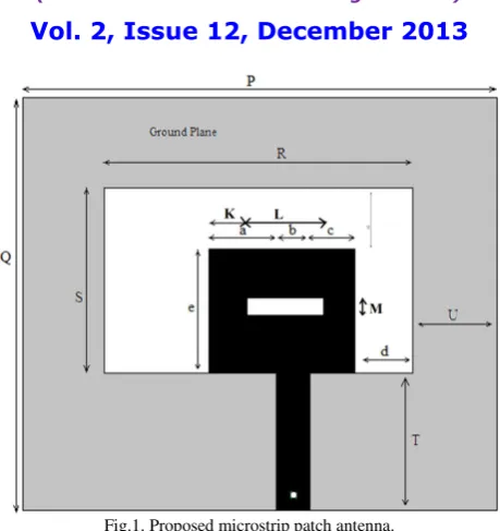
Fig.1. Proposed microstrip patch antenna.
Table 1: Geometric dimension of Figure 1 and 2(all dimensions are in mm)
Parameters Dimension Parameters Dimension
P
54
K
5
Q
60
L
15
R
45
M
3
S
29
a
14
T
20
b
4
U
4
c
5
V
18
d
8
W
30
e
20
V
9
-
-
III.ANRENNARESULTS
ISSN: 2319-8753
I
nternational
J
ournal of
I
nnovative
R
esearch in
S
cience,
E
ngineering and
T
echnology
(An ISO 3297: 2007 Certified Organization)
Vol. 2, Issue 12, December 2013
Fig.2. Return losses versus Frequency of the antenna.
ISSN: 2319-8753
I
nternational
J
ournal of
I
nnovative
R
esearch in
S
cience,
E
ngineering and
T
echnology
(An ISO 3297: 2007 Certified Organization)
Vol. 2, Issue 12, December 2013
Fig.4. VSWR versus frequency of proposed antenna.
ISSN: 2319-8753
I
nternational
J
ournal of
I
nnovative
R
esearch in
S
cience,
E
ngineering and
T
echnology
(An ISO 3297: 2007 Certified Organization)
Vol. 2, Issue 12, December 2013
Fig.6. Current distribution at V=10 mm, V=11 mm, V=12 mm and V=13 mm.
IV.CONCLUSION
The compact microstrip has been designed using Ansoft designer. The simulated results show that the return loss, VSWR, swept gain due to variation of slits dimension. Measured results have been obtained using standard microwave test bench. This antenna may be used for radar and wireless communications system. It has been observed that the proposed antenna exhibits maximum bandwidth 148%. It has covered multi frequency band from 1.34 GHz to 8.1 GHz. The maximum gain 3.2dBi is achieved at the resonant frequency of 4.58 GHz.
REFERENCES
[1] Sappan, “A new broadband stacked two layered microstrip antenna”, IEEE Trans. Microw. Theory Tech, Vol. 40, pp.769, 1991.
[2] L. Mo, H. Zhang, and H. Zhou, “ Broadband UHF RFID tag antenna with a pair of U slots mountable on metallic objects”, Electron Letter Vol.44, pp. 1173–1174, 2008.
[3] S.L. Chen, and K.H. Lin, “A slim RFID tag antenna design for metallic object applications”, Antennas Wireless Propagation Letter Vol.7, pp.729–732, 2008.
[4] L. Mo, H. Zhang, and H. Zhou, “Broadband UHF RFID tag antenna with a pair of U slots mountable on metallic objects”, Electron Letter, Vol.44, pp. 1173–1174, 2008.
[5] L.K. Anderson, “An analysis of broadband circulators with external tuning elements”, IEEE Trans MTT, Vol.15, pp 42–47, 1967.
[6] T. Miura, M. Kobayashi, and Y. Konishi, “Optimization of a lumped element circulator based on eigenvalue evaluation and structural improvement,” IEEE Trans MTT, Vol. 44, pp. 2648–2654, 1996.
[7] J.O. Bergman, “Equivalent circuit for a lumped-element Y circulator”, IEEE Trans MTT 16 (1968), 308–310.
[8] R.H. Knerr, “An improved equivalent circuit for the thin-film lumped element circulator,” IEEE Trans MTT, Vol. 20, pp. 446–452, 1972. [9] J.L. Young, R.S. Adams, B. O’Neil, and C.M. Johnson, “ Bandwidth optimization of an integrated microstrip circulator and antenna assembly:
Part 2”, IEEE Antennas Propag Mag Vol.49, pp. 82–91, 2007.
[10] W.L. Stutzman and G.A. Thiele, “Antenna theory and design", 1st ed., John Wiley and Sons, New York, pp. 260, 1981.