Single Cycle Risc Micro Architecture Processor
Using Clock Gating Technique
T.Subhashini, M.Kamaraju, K.Babulu
Abstract: In this paper investigates development of a fully synthesizable 32-bit processor based on the open-source RISC-ISA. Open source Instruction Set Architecture (ISA)s are available in market to design a processor. The main purpose of this processor is to make low cost embedded devices. RISC based architectures are widely used to achieve low power. This work presents designing of single cycle RISC micro-architecture processor using clock gating technique. To design this processor RISC-16 ISA is used. The proposed processor is having a single core, with low hardware complexity. It is developed using Verilog HDL. The Xilinx ISE 13.2 tool used to implement this processor and power is estimated by using Xilinx Power Analyzer. In this work single stage and two stages clock gating techniques are applied and verified power and delays of the designed processor. This processor targeted on Xilinx FPGA device.
Index Terms: RISC,RISC ISA, Micro-architecture, low power, clock gating technique, single core, single cycle. —————————— ——————————
1.
INTRODUCTION
The VLSI is a process of VLSI is a process of creating an integrated circuit in which millions of transistors or devices are placed. VLSI began in 1970s at that time complex
semiconductor and communication technologies were
developed. Most ICs have limited set of functions they can perform. An electronic circuit consists of CPU, ROM, RAM and other glue logic. VLSI allows IC designers add all of these into one chip. The electronics industry has achieved rapid growth over the past few decades due to the rapid advances in large scale integration technologies and system design applications. Because of the popularity of very large scale integration (VLSI) design, the number applications of integrated circuits(ICs) in different fields like high performance computing, controls, telecommunications, image and video processing, and consumer electronics has been increased. We go for VLSI because of integration improves the design. Integration provides compactness means less area, physically smaller. It provides higher speed by offering lower parasitic means reduced interconnection length. It offers lower power consumption. It offers higher reliability by providing improved on-chip interconnects. Integration reduces the manufacturing cost. Microprocessor is defined as a programmable electronics chip, which has computing and decision making capabilities like central processing unit of a computer. Any microprocessor based systems which are having resources limited in number are known as microcomputers. Nowadays, almost all kinds of electronic devices contain microprocessor. Examples for these systems are mobile phones, washing machines, printers etc. Advanced applications are also used microprocessors like satellites, radars, flights etc. Because of the rapid advancements, which took place in electronic industry and large scale integration of devices leads to a remarkable cost reduction and it also leads to an increase in applications which are using microprocessors and derivatives of microprocessors. Microprocessor consists of arithmetic and logic unit (ALU) in combination with control unit to execute an instruction. If the processor executes an instruction in more than one cycle then the execution is called as multi cycle execution [1]. If the processor executes an instruction in one cycle then the execution is called as single cycle execution. Microprocessors are working depending upon the principle called store-program concept. In this concept programs and instruction stored sequentially in the memory locations which are need to be executed.
Classification of Microprocessor:
According to the specification, application and architecture microprocessors are classified.
Depend on Data Bus size: According to size of data bus microprocessors are available in 4-bit, 8-bit, 16-bit, 32-bit etc.
Depend on application: According to application
Microprocessors are of 3 types. They are
1. General purpose microprocessor: It can be programmed for any application by the programmer.
Ex: 8085 to Intel Pentium.
2. Micro controller: It is a microprocessor having in built memory and ports. It is programmed for control applications
Ex: 8051
Special-purpose processors: These are manufactured to deal with special functions, which are required by an application. Ex: application specific integrated circuit (ASIC) chips, digital signal processor.
Depend on architecture: According to the architecture microprocessors are of 2 types
1. Reduced instruction set computer (RISC) processors.
2. Complex instruction set computer (CISC) processors.
2327 instruction set, number of instruction cycles and cost while
implementing a design [5]. Development of silicon technology and reduction in the prices of integrated circuits leads to increase in the usage of RISC processors in all fields [5]. Advantages of RISC Processors:
It is giving support to optimize the architectural aspects, which are most used and most time consuming.
Design complexity is very less in RISC
Design cost is reduced in RISC
In design process the time between designing and
marketing is reduced.
It is easy to design and gives better performance.
Chip space used is very less because of reduced
instruction set.
This paper is presented as follows Section II describes single cycle RISC-V micro-architecture processor and its FPGA prototype. Section III describes single cycle RISC micro-architecture processor using clock gating technique. Section IV describes implementation. Section V presents the results. Section VI presents conclusion.
2 SINGLE
CYCLE
RISC-V
MICRO
ARCHITECTURE
PROCESSOR
AND
ITS
FPGA
PROTOTYPE
2.1 Introduction:
In this work, fully synthesizable 32-bit processor and its development by using the open-source Instruction Set Architecture (ISA) called RISC-V (RV32I) is described. The purpose of this processor design is to get embedded devices with low cost. The development of RISC-V processor is presented in this work. Then we get the single core processor, which is in-order and non-bus based. This processor is having low complexity of hardware. RISC-V ISA is an open source ISA. Some ISAs are available as open source ISA [6]. This processor is implemented by using the hardware description language called Verilog HDL, after that it is prototyped on FPGA board named as ―Spartan 3E XC3S500E‖. FPGA provides quick time to market [7]. The maximum operating frequency 32MHz is resulted from this work. The power 7.9mW is estimated to get from the design. Xilinx Power Analyzer is used to get power of the design. A large number of
embedded applications use 32-bit processor. These
applications require small embedded processor. To analyze the performance single cycle design is used.
2.2 Block diagram
The block diagram of RISC-V processor shown in figure 1.,the processor core is divided into four logical modules. The block which has fetch, decode and control logic is used to fetch and decode the instruction from the instruction memory and then the corresponding control signals are generated from this block. The target addresses of jump instructions and branch instructions are solved by this block. This block has the program counter, control unit, the target address selection logic, the instruction decoder, and instruction memory controller. It has an adder to increment the PC in every cycle. Separate signals are provided for both exceptions, which are internal exceptions and external exceptions. The module which contains ALU logic and Register Bank has read and write logic, the register addressing, 31 general purpose registers and arithmetic logic unit (ALU). In this block ALU do operations related to register-register and register-immediate, which are arithmetic operations. For ALU to perform the operation register-immediate 32-bit reordered and correctly sign extended immediate operand is provided by the block which has shift and shuffle logic and sign extension and register bank provides second operand. The address calculation of branch and jump instructions is not done by ALU for that specified adders are used. ALU measures condition in branch instructions and then the corresponding results are given to the control unit to decide if a branch is to be taken. To reduce critical path delay ALU is placed nearer to the register bank. Here five kinds of immediate formats are used. They are I, S, B, U and J-type. Immediate instructions are encoded after encoding it has shuffled bits. In decoding process immediate values are properly reordered, left shifted or sign extended. This type of encoding is used to reduce complexity involved in implementation of ISA extensions. The block which has shift and shuffle logic and sign extension handles this type of immediate decoding. The block which has memory and control logic has different store and load operations which contain addresses belong to data memory. These addresses are word aligned addresses and misaligned addresses.
2.3 Micro Architecture
The figure 2 micro architecture shows the architecture data path implementation and control path implementation. Three inputs are accepted by the control unit (CU). They are opcode (0 to 6 bits), funct3 (12 to 14 bits) and the 30th bit of the instruction. Based on the three inputs it sends various control signals to various modules to choose and to execute instructions correctly. Control unit provides 12 control lines. Fig. 1. Block Diagram of RISC V Processor.
For example, ALU Ctrl (4-bit) is used to direct ALU to perform required operation on its operands. Reg WR (1-bit) is used to keep the register file in two modes that are write mode and read mode. If the bit is 1 it is in write mode or if the bit is 0 it is in read mode. Like that, controlling of all the modules is to be done. The block which has shift and shuffle logic and sign extension consists of one left shift module, two sign extending modules and two sign extend and shuffle module. The SIGN EXTN.1 module handles 12-bit, I-type immediate and the SIGN EXTN.2 module handles 12-bit, S-type immediate. After encoding the immediate S-type it gives the instruction with two disintegrate segments which is the difference between this immediate and the immediate I-type. Instructions which are U-type are used the SHIFT LEFT 12 block. These instructions are used to encode 20-bit immediate. Most significant 20-bits are used this immediate. So it is shifted left by 12. The blocks called SIGN EXTN & SHUFFLE are in active state for control transfer instructions such as J-type and B-type.In the block which has shift and shuffle logic and sign extension the immediate in the instructions are encoded in encoding process and then reordered when these are decoded and sign extended according to the requirement of ISA. Instruction memory and data memory maximum allowable size is 4GB, but for simulation process instruction memory size is chosen as 64KB and data memory is chosen as 16KB. 32 registers, which are of 32-bit width, are present in the register file. The instruction called jal is used to access program counter (particularly, program counter + 4) by giving offset value is 0. The store block has word aligned addresses at which the data is written one word at a time. Then it evaluates the correct word aligned address and it also evaluates the offset which is present in the word at the same address, if there is any misaligned instructions such as store word/half/byte are come. As an example, if the store byte (SB) instruction which is misaligned occurs, store logic recognizes the corresponding word aligned address of the byte and its offset in the word. The word which has the required byte is read from data memory with the help of word aligned address which is already calculated. It can create a new word with the help of calculated offset and by following the procedure called masking of the bits without altering the bits. The new word is again stored back in the memory. Similarly word aligned address of load instruction and its offset is calculated by load block. It reads the required word and then it shifts the half word or it shifts the byte within the word towards least significant bits according to the requirement and then sign extends or zero extends according to ISA specifications. Due to single cycle behavior of the design it requires a redundancy level to get balance in reuse of components between instructions and to get balance of critical path length. Hence an adder is used additionally to calculate branch target and five I-type instructions have their own sign-extension and reordering modules. To increment its value a specified adder is used for program counter. The program counter calculates the instruction address, which is to be executed. Instruction gives the needed inputs to the register file, the module which has shift and shuffle logic and sign extension and the control unit (CU). CU controls each module by sending signals. Source registers and destination register (rs1, rs2 and rd) addresses are given to the register file by the instruction. An operation is performed on inputs of a particular instruction by the ALU which is indicated by multiplexers and controlled by the module called control unit (CU). Control unit provides
control bits, based on the bits ALU output is stored in register file, data memory and program counter according to the type of instructions. In load and store instructions it is stored in data memory, in jump instructions it is stored in program counter. Program counter address is specified by the multiplexer. The demerits of this system are lack of integrating I/O bus, lack of
multilevel cache mechanism, lack of floating point
coprocessor.
3
SINGLE
CYCLE
RISC
MICRO
ARCHITECTURE
PROCESSOR
USING
CLOCK
GATING
TECHNIQUE
3.1 Introduction
2329 short word addresses means address 0 refers to first two
bytes of main memory, address 1 refers to second two bytes of main memory. Same as MIPS instruction set architecture register 0 has always 0 value. Register 0 will always return 0 whatever the value stored there. RISC-16 is very simple and it solves complex problems. It has 3 machine code instruction instruction formats and 8 instructions.
3.2 Clock gating technique
In proposed processor design clock gating technique will be used to reduce the power consumption of the processor. Here clock gating and two stage clock gating both are applied to the processor to reduce power consumption. Clock gating technique is a widely used technique in synchronous circuits to reduce dynamic power dissipation. Dynamic power consumption is due to charging and discharging of capacitances in the circuit. Clock gating adds more logic to the required circuit to save power. In this technique clock disables some components of the circuit, which are not required for the operation. Because of that flip-flops in such components no need to switch between states. There is no switching of states, so power consumption will be reduced. For that reason switching power of the circuit becomes zero. Clock gating works depending upon the enable conditions, used in the registers. These enable conditions are used to gate the clocks. So a design must have enable conditions to get the advantage of clock gating. Clock gating also saves die area along with power. If clock gating logic is applied to the circuit, it removes large number of multiplexers. Because of that reason die area will be saved.
3.3 RISC Processor using Clock Gating
The figure 3 shows the block diagram of RISC processor using clock gating shows the blocks used in the design of single cycle RISC processor using clock gating. The modules used here are adder, register, counter, ALU, accumulator, clock gating, machine control, and machine. In which modules are applied with clock gating to put them in off state whenever no need to use them to reduce clock power, which leads to reduction in power consumption.
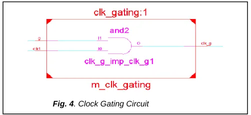
The figure 4 shows the clock gating operation the working of clock gating technique. It has two inputs signals. They are input signal 1 and input signal 2. It has one output signal. The output of this circuit is AND operation of two input signals.
3.2 RISC Processor using Two stage Clock gating technique
The figure 5 block diagram of RISC processor using two stage clock gating shows the block diagram of single cycle RISC processor using two stage clock gating. Here two stage clock gating is applied to the modules to put them in off state whenever not necessary in the processor operation to reduce the clock power further. Hence the power consumption of the processor will be reduced.
Two stage clock gating circuit:
The two stage clock gating operation shows in figure 6 and the working of two stage clock gating. it has two input signals. They are input signal 1 and input signal 2. It has one output Fig. 3. Block Diagram of RISC Processor Using Clock Gating.
Fig. 4. Clock Gating Circuit
Fig.5. Block Diagram of RISC Processor using Two stage clock gating.
signal. In which clock gating is applied two times. In first stage we get clock gated signal. This signal is again applied with clock gating. Hence we obtain the two stage clock gated signal as output.
3.3 RISC Micro Architecture
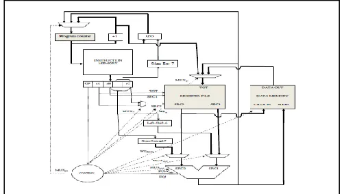
The figure 7 shows micro architecture of single cycle RISC processor describes the information flow of each instruction of the processor. Here the shaded boxes indicate registers. Thick lines indicate 16-bit buses.
Th figure 7 shows the micro architecture of single cycle RISC processor describes all the data and control paths of the processor. To handle all these paths a number of multiplexers are required to choose the direction of dataflow. These multiplexers are operated by the CONTROL module, which is based on two inputs.
1. 3-bit OPCODE of the instruction 2. 1-bit EQ! Signal from the ALU
1-bit EQ! Is used only for BEQ instruction, which declare that the two operands are equal for remaining instructions this signal is not considered. The CONTROL module is needed to be a decoder. It accepts the two input signals and sets different output signals, which control ALU, a number of multiplexers contained in the processor, and writes functions of register file and data memory. For each cycle beginning program counter stores new value it fetch new instruction from instruction memory and it sends new opcode to the CONTROL module. It sets the control signals according to the instruction.
4
IMLEMENTATION
4.1 Tools
Introduction:
The tool required for this work is Xilinx ISE 13.2. In which verilog source code is easily used to implement a design. Xilinx software is a package of software tools which are used to design a digital circuit and implemented the digital circuits using Field Programmable Gate Array (FPGA) or Complex Programmable Logic Device (CPLD). The different steps involved in design procedure are a) design entry, b) synthesis and implementation of the design, c) functional simulation and d) testing and verification. In this work Spartan 3E FPGA’s are used. Device used in this work is XC3S100E. Package used in this work is VQ100. Speed grade is ―-5‖. Synthesis tool used is
XST (Xilinx Synthesis Technology). Simulator used is Xilinx ISE Simulator. The major processes involved while implementing this work are synthesis and simulation.
Synthesis:
In this process the entire HDL code is converted into net list form and then the net list will be saved as an NGC (Native Generic Circuit) file. During implementation process NGC process through translate, map, place and route steps. In translate step NGC file converted into NGD (Native Generic Database) file, next in map step NGD file converted into NCD (Native Circuit Description) file. In place and route step mapped NCD file is become route NCD file. After that device is programmed and then design verified to get static timing analysis and simulation. Here we got the timing report and device utilization summary.
Simulation:
In this process functional verification of the design will be done for correctness of the required operation. In this process we can observe the output waveforms for different inputs according to our requirement.
4.2 Flow charts
The figure 8 shows the flow chart of clock generator describes the operation of clock generator module. It generates the clock signal according to the condition. If reset value is 0, it goes to states from 1to 8 and do operations in the respective states and then goes to idle state. If reset value is 1, it directly goes to idle state.
Fig.7 Micro Architecture for a single cycle RISC processor.
Fig. 8. Clock generator flow diagram
2331 IJSTR©2019
The figure 9 shows the flow chart of clock gating describes the operation of clock gating module. The output of this module is AND operation of inputs clk1 and g. if output value is 1, it applies gating to a particular module according to the requirement.
The two stage clock gating describes the operation of two stage clock gating module shown in figure 10. In this module clock gating is applied two times. In which clock gated clock is again applied with the clock gating. Then we get two stage clock gating. The output of this module is AND operation of clk_g1 and g. if output value is 1, it applies gating to a particular module according to our requirement.
The figure 11 flowchart of ALU describes the operation of ALU module. The ALU performs the operation on given data according to the condition. If opcode value is unknown by default ALU output is an unknown state. If opcode value is known, depending upon that value the arithmetic and logical operations are performed by ALU according to the operation ALU output value will be known.
The figure 12 shows flowchart of machine control describes the operation of machine control module. According to the condition machine control module works. If reset value is 0, then enable value is 1. If reset value is 1, then enable value is 0. According to the enable value it controls the machine.
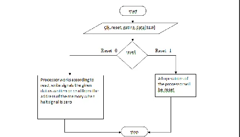
The figure 13 shows flowchart of machine describes the operation of machine module. It works based on the condition. If enable value is 0, then state is 0 and all the outputs will be 0. If enable value is 1, it goes to states from 0 to 7. The corresponding operations of each state will be done by this machine, when it goes to that particular state. The figure 14 shows the flow chart of RISC processor operation describes the operation of the processor. It works based on the condition. If reset value is zero then only the processor works according to our requirement whether it is read or write operation, the given data is written or read from memory when halt signal value is zero. If halt value is 1 the processor operation will be stopped. If reset value is 1 the processor operations will be cleared and it comes to initial state.
5
RESULTS
5.1 Simulation Results
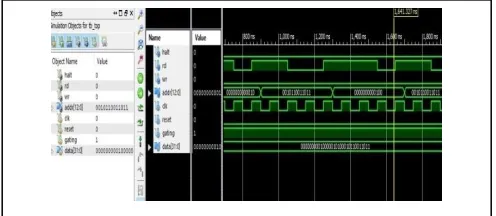
The simulation waveforms of conventional processor, shows in the figure 15 and the working of conventional processor. In which clk, reset, gating, and data are input signals. The output signals are halt, rd, wr, and addr. The processor sends the data to the corresponding address based on read and write operations. If halt signal is 1 then the processor stops operation. If reset is 1 all the operations of the processor are cleared and processor comes to its initial state. If gating is 1 Fig. 10. Two stage clock gating flow diagram
Fig. 11. ALU operation flow diagram
Fig. 12. Machine control flow diagram
Fig. 13. Machine flow diagram
the processor is applied with clock gating to reduce power consumption of it.
The figure 16 shows the simulation waveforms of RISC processor using clock gating technique, shows the working of clock gated RISC processor. In which clk, reset, gating, and data are input signals. The output signals are halt, rd, wr, and addr. The processor sends the data to the corresponding address based on read and write operations. If halt signal is 1 then the processor stops operation. If reset is 1 all the operations of the processor are cleared and processor comes to its initial state. If gating is 1 the processor is applied with clock gating to reduce power consumption of it.
The figure 17 shows the simulation waveforms of RISC processor using two stage clock gating, shows the working of two stage clock gated RISC processor. In which clk, reset, gating, and data are input signals. The output signals are halt, rd, wr, and addr. The processor sends the data to the corresponding address based on read and write operations. If halt signal is 1 then the processor stops operation. If reset is 1 all the operations of the processor are cleared and processor comes to its initial state. If gating is 1 the processor is applied with clock gating to reduce power consumption of it.
5.2 Synthesis Results
The figure 18 shows the RTL schematic of conventional processor shows the register transfer level graphical representation of conventional processor. It is a gate level schematic of the design represented in symbols as AND gates, OR gates, counters, multipliers, and adders.
The figure 19 shows RTL schematic of RISC processor using clock gating shows the clock gated RISC processor design at register transfer level. It is a gate level schematic of the design represented in symbols as AND gates, OR gates, counters, multipliers, and adders.
The figure 20 shows the RTL schematic of RISC processor using two stage clock gating shows the two stage clock gated RISC processor design at register transfer level. It is a gate level schematic of the design represented in symbols as AND gates, OR gates, counters, multipliers, and adders.
The figure 21 shows the technology schematic of RISC processor using clock gating shows the design of clock gated RISC processor in terms of logical elements like look up table (LUT) s, buffers and other technology specific elements. It is used to identify the design issues if any during the design process.
Fig. 15. Simulation waveforms of Conventional processor
Fig. 16. Simulation waveforms of RISC processor using clock gating
Fig. 17. Simulation waveforms of RISC processor using two satge clock gating
Fig. 19. RTL Schematic of RISC Processor using clock gating Fig. 18. RTL Schematic of Conventional Processor
2333 The figure 22 shows the technology schematic of RISC
processor using two stage clock gating shows the design of two stage clock gated RISC processor in terms of logical elements like look up table (LUT) s, buffers and other technology specific elements. It is used to identify the design issues if any during the design process.
5.3 Graphs
The figure 23 shows the graph of voltage vs. power at fixed frequency shows the relation between voltage and power of conventional processor, clock gated RISC processor, two stage clock gated RISC processor at fixed frequency.
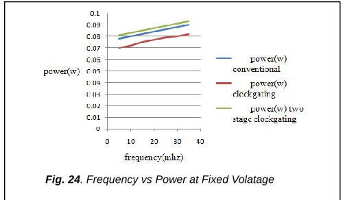
The figure 24 shows the graph of frequency vs. power at fixed voltage shows the relation between frequency and power of conventional processor, clock gated RISC processor, two stage clock gated RISC processor at fixed voltage.
The figure 25 shows the graph of frequency vs. power at fixed capacitance shows the relation between frequency and power of conventional processor, clock gated RISC processor, two stage clock gated RISC processor at fixed capacitance.
5.4 Comparison between Processors
The table 1 shows the comparison of processors gives the details of number of components used in the design of conventional processor, clock gated RISC processor, two stage clock gated RISC processor and power consumption of the respective processors.
6 CONCLUSIONS
In this work Single Cycle 32-bit RISC micro architecture processor by using Clock gating technique is designed. The processor is designed to get low power and low cost embedded devices with less complexity. The processor
TABLE1
COMAPRISION OF PROCESSORS
Fig. 21. Technology Scematic of RISC Processor Clock gating
Fig. 22. Technology Scematic of RISC Processor using two stage Clock gating
Fig. 23. Voltage Vs Power at fixed frequency
Fig. 24. Frequency vs Power at Fixed Volatage
consumes the total power of 0.078w. Here clock gating technique is used to reduce the processor power consumption. This processor is implemented on Spartan 3EXC3S100E. The delay of this processor will not change even though increase in the stages of processor in two stage clock gating.
REFERENCES
[1] Mohammad Zaid, and Prof. Pervez Mustajab, ―Design and
Application of RISC Processor‖, International conference on Multimedia, Signal Processing and Communication Technologies (IMPACT), NOV 2017, IEEE.
[2] Agineti Ashok, and V. Ravi, ―ASIC design of MIPS based
RISC processor for high performance‖, International conference on Nextgen Electronic Technologies: Silicon to software (ICNETS2), March 2017, IEEE.
[3] Raj Prakash Singh, Ankit K Vashishtha, and Krishna R, ―
32 bit Reconfigurable RISC Processor Design and Implementation for BETA ISA with Inbuilt Matrix Multiplier‖, sixth International Symposium on Embedded Computing and System Design(ISED), Dec 2016, IEEE.
[4] P.V.S.R. Bharadwaja, K. Ravi Teja, M. Naresh babu, and
K. Neelima, ―Advanced Low Power RISC Processor Design using MIPS Instruction Set‖, IEEE second
International Conference on Electronics and
Communication Systems(ICECS), July 30, 2016.
[5] Jikku Jeemon, ―Pipelined 8-bit RISC Processor Design using Verilog HDL on FPGA‖, IEEE international conference on Recent Trends in Electronics Information Communication Technology (RTEICT), May 2016.
[6] Aneesh Raveendran, Vinayak Baramu Patil, David
Selvakumar, and Vivian Desalphine, ―A RISC-V Instruction Set Processor-Micro-architecture Design and Analysis‖, International conference on VLSI Systems, Architectures, Technology and Applications (VLSI-SATA), Jan 2016, IEEE.
[7] S.P. Ritpurkar, M.N. Thakare, and G.D. Korde, ―Design and Simulation of 32-bit RISC architecture based on MIPS using VHDL‖, International Conference on Advanced Computing and Communication Systems, Jan 2015, IEEE.
[8] V. Patil, A. Raveendran, P. M. Sobha, A. D. Selvakumar, and D. Vivian, ―Out of order floating point coprocessor for risc v isa,‖ in 2015 19th
International Symposium on VLSI Design and Test, June 2015, pp. 1–7
[9] A. Waterman, Y. Lee, D. A. Patterson, K. Asanovic, V. I. U. level Isa, A. Waterman, Y. Lee, and D. Patterson, ―The risc-v instruction set manual,‖ 2014 .
[10]Samiappa Sakthikumaran, S. Salivahanan, and V.S.
Kanchana Bhaaskaran, ―16-bit RISC Processor Design for Convolution Application‖, International Conference on Recent Trends in Information Technology (ICRTIT), June 2011, IEEE.
[11]Xunying Zhang, Xubang Shen, ―A Power-Efficient
Floatingpoint Co-processor Design‖, 2008 International
Conference on Computer Science and Software
Engineering
[12]ARM Ltd. ARMv6-M Architecture Reference Manual,
2008.
[13]S. P. Dandamudi, Guide to RISC Processors: For
Programmers and Engineers. Secaucus, NJ, USA: Springer-Verlag New York, Inc., 2005.
[14]C. Jeong, S Kim, M Lee ―In-Order Issue Out-of-Order Execution Floating-point Coprocessor for CalmRISC32‖. 15th IEEE Symposium on Computer Arithmetic, 2001 [15]Don Kurian Dennis, Ayushi Priyam, Sukhpreet Singh Virk,
Sajal Agrawal, Tanuj Sharma, Arijit Mondal and Kailash Chandra Ray, ―Single Cycle RISC-V Micro Aachitecture Processor and its FPGA Prototype‖, 7th