Multi-Level Simulation of
Nano-Electronic Digital Circuits
on GPUs
Von der Fakultät Informatik, Elektrotechnik und Informationstechnik der
Universität Stuttgart zur Erlangung der Würde eines Doktors der
Naturwissenschaften (Dr. rer. nat.) genehmigte Abhandlung
Vorgelegt von
Eric Schneider
aus Hildburghausen, Deutschland
Hauptberichter: Prof. Dr. rer. nat. habil. Hans-Joachim Wunderlich
Mitberichter:
Prof. Dr. phil. nat. Rolf Drechsler
Tag der mündlichen Prüfung: 21. Juni 2019.
Institut für Technische Informatik der Universität Stuttgart
2019
Contents
Acknowledgments ix
Abstract xi
Zusammenfassung xiii
List of Abbreviations xxi
1 Introduction 1
I Background
2 Fundamental Background 13
2.1 CMOS Digital Circuits . . . 13
2.1.1 CMOS Switching and Time Behavior . . . 14
2.1.2 Circuit Performance and Reliability Issues . . . 16
2.2 Circuit Modeling . . . 17 2.2.1 Electrical Level . . . 18 2.2.2 Switch Level . . . 19 2.2.3 Logic Level . . . 20 2.2.4 Register-Transfer Level . . . 23 2.2.5 System-/Behavioral Level . . . 23 2.3 Delay Faults . . . 23
2.4 Circuit and Fault Simulation . . . 28
2.5 Multi-Level Simulation . . . 31
2.6 Summary . . . 32
3 Graphics Processing Units (GPUs) 33 3.1 GPU Architecture . . . 33 3.1.1 Streaming Multiprocessors . . . 35 3.1.2 Thread Scheduling . . . 36 3.1.3 Memory Hierarchy . . . 37 3.2 Programming Paradigm . . . 38 3.2.1 Thread Organization . . . 40 3.2.2 Memory Access . . . 41 3.3 Summary . . . 42
4 Parallel Circuit and Fault Simulation on GPUs 43 4.1 Overview . . . 43
4.2 Parallel Circuit Simulation . . . 44
4.3 Parallel Gate Level Simulation . . . 45
4.3.1 Logic Simulation . . . 46
4.3.2 Timing-aware Simulation . . . 47
4.4 Parallel Fault Simulation . . . 49
4.5 Summary . . . 52
II High-Throughput Time and Fault Simulation 5 Parallel Logic Level Time Simulation on GPUs 57 5.1 Overview . . . 57
5.2 Circuit Modeling . . . 58
5.2.1 Gates . . . 60
5.2.2 Delay . . . 61
5.2.3 Variations . . . 62
5.3.1 Events and Time . . . 64 5.3.2 Delay Processing . . . 65 5.3.3 Waveforms . . . 66 5.4 Algorithm . . . 69 5.4.1 Serial Algorithm . . . 69 5.4.2 Parallelization . . . 74 5.5 Implementation . . . 78 5.5.1 Waveform Allocation . . . 80 5.5.2 Kernel Organization . . . 82 5.5.3 Simulation Flow . . . 86
5.5.4 Test Stimuli and Response Conversion . . . 88
5.6 Summary . . . 92
6 Parallel Switch Level Time Simulation on GPUs 93 6.1 Overview . . . 93
6.2 Switch Level Circuit Model . . . 95
6.2.1 Channel-Connected Components . . . 95
6.2.2 RRC-Cell Model . . . 97
6.2.3 Switch Level Waveform Representation . . . 99
6.2.4 Modeling Accuracy . . . 103
6.3 Switch Level Simulation Algorithm . . . 103
6.3.1 RRC-Cell Simulation . . . 104
6.4 Implementation . . . 111
6.5 Summary . . . 113
7 Waveform-Accurate Fault Simulation on GPUs 115 7.1 Overview . . . 115
7.2 Fault Modeling . . . 116
7.2.1 Small Gate Delay Fault Model . . . 117
7.2.2 Switch-Level Fault Models . . . 118
7.2.3 Fault Injection . . . 121
7.3.2 Discrete Syndrome Computation . . . 123 7.3.3 Fault Detection . . . 124 7.4 Fault-Parallel Simulation . . . 126 7.4.1 Fault Collapsing . . . 126 7.4.2 Fault Groups . . . 128 7.4.3 Grouping Algorithm . . . 129
7.4.4 Parallel Fault Evaluation . . . 132
7.5 Summary . . . 134
8 Multi-Level Simulation on GPUs 135 8.1 Overview . . . 135
8.2 Multi-Level Circuit Modeling . . . 137
8.2.1 Region of Interest . . . 137
8.2.2 Changing the Abstraction . . . 138
8.2.3 Mixed-abstraction Temporal Behavior . . . 138
8.2.4 Simulation Flow . . . 140
8.3 Transparent Multi-Level Time Simulation . . . 142
8.3.1 Waveform Transformation . . . 143
8.4 Multi-Level Data Structures and Implementation . . . 147
8.4.1 Multi-Level Node Description . . . 148
8.4.2 Multi-Level Netlist Graph . . . 149
8.4.3 Multi-Level Waveforms . . . 150
8.4.4 Parallelization . . . 151
8.5 Summary . . . 152
III Applications and Evaluation 9 Experimental Setup 155 9.1 Benchmarks . . . 155
9.2 Host System . . . 156
9.4 Data Representation . . . 158
9.5 Performance Metrics . . . 158
10 High-Throughput Time Simulation Results 161 10.1 Logic Level Timing Simulation Performance . . . 161
10.1.1 Runtime Performance . . . 162
10.1.2 Simulation Throughput . . . 164
10.2 Switch Level Timing Simulation Performance . . . 166
10.2.1 Runtime Performance . . . 166
10.2.2 Throughput performance . . . 167
10.3 Switch Level Behavior . . . 170
10.4 Summary . . . 172
11 Application: Fault Simulation 175 11.1 Fault Grouping Results . . . 176
11.2 Small Delay Fault Simulation . . . 178
11.2.1 Variation Impact . . . 179
11.3 Switch Level Fault Simulation . . . 180
11.3.1 Resistive Open-Transistor Faults . . . 181
11.3.2 Capacitive Faults . . . 183
11.4 Summary . . . 185
12 Application: Power Estimation 187 12.1 Circuit Switching Activity Evaluation . . . 187
12.1.1 Weighted Switching Activity for Power Estimation . . . 188
12.1.2 Distribution of Switching Activity . . . 189
12.1.3 Correlation of Clock Skew Estimates . . . 190
12.2 Summary . . . 194
13 Application: Multi-Level Simulation 195 13.1 Multi-Level Simulation Runtime . . . 195
13.2 Multi-Level Trade-Off . . . 197
13.2.3 Simulation Efficiency . . . 199 13.3 Summary . . . 201 Conclusion 203 Bibliography 205 A Benchmark Circuits 227 B Result Tables 229 List of Symbols 235 Index 237
Acknowledgments
I would like to thank Prof. Hans-Joachim Wunderlich for giving me the opportunity to work at theInstitut für Technische Informatik(ITI) in Stuttgart and to let me experience the life in academia under his professional supervision. I am deeply grateful for his invaluable patience and faith in me, as well as the countless and very often insightful discussions we had. Furthermore, I want to thank Prof. Rolf Drechsler from University of Bremen for taking over the role as my second adviser and also for the nice chats.
In addition, I am very grateful to Stefan Holst, who was my mentor during my undergrad-uate studies and who helped me getting started at the ITI as a colleague and friend. I very much enjoyed the work with the other colleagues and friends as well, which alto-gether made the life at the institute interesting and enjoyable in many ways. Therefore I am happy to thank Michael A. Kochte and Claus Braun as well as Laura Rodrígez Gómez, Dominik Ull, Chang Liu, Rafał Baranowski, Alexander Schöll, Michael Imhof, Abdullah Mumtaz, Marcus Wagner, Sebastian Brandhofer, Ahmed Atteya, Natalia Lylina, Zahra Paria Najafi Haghi and Chih-Hao Wang. I also want to thank Lars Bauer from Karlsruhe Institute of Technology, Matthias Sauer formerly from University of Freiburg, Prof. Sybille Helle-brand and Matthias Kampmann from University of Paderborn as well as Prof. Xiaoqing Wen and Kohei Miyase from Kyushu Institute of Technology and Yuta Yamato formerly from Nara Institute of Science and Technology for all the insightful discussions and col-laborations we could establish together.
Thank you, Mirjam Breitling, Lothar Hellmeier and Helmut Häfner. Without your admin-istrative and technical assistance this work would have been impossible for me.
Last but not least, I am also very grateful to my parents for their constant support and caring.
Stuttgart, June 2019 Eric Schneider
Abstract
Simulation of circuits and faults is an essential part in design and test validation tasks of contemporary nano-electronic digital integrated CMOS circuits. Shrinking technology processes with smaller feature sizes and strict performance and reliability requirements demand not only detailed validation of the functional properties of a design, but also accurate validation of non-functional aspects including the timing behavior. However, due to the rising complexity of the circuit behavior and the steady growth of the designs with respect to the transistor count, timing-accurate simulation of current designs requires a lot of computational effort which can only be handled by proper abstraction and a high degree of parallelization.
This work presents a simulation model for scalable and accurate timing simulation of digital circuits on data-parallelgraphics processing unit(GPU) accelerators. By providing compact modeling and data-structures as well as through exploiting multiple dimensions of parallelism, the simulation model enables not only fast and timing-accurate simulation at logic level, but also massively-parallel simulation with switch level accuracy.
The model facilitates extensions for fast and efficient fault simulation of small delay faults at logic level, as well as first-order parametric and parasitic faults at switch level. With the parallelization on GPUs, detailed and scalable simulation is enabled that is applicable even to multi-million gate designs. This way, comprehensive analyses of realistic timing-related faults in presence of process- and parameter variations are enabled for the first time. Additional simulation efficiency is achieved by merging the presented methods in a unified simulation model, that allows to combine the unique advantages of the different levels of abstraction in a mixed-abstraction multi-level simulation flow to reach even higher speedups.
dented simulation throughput as well as high speedup compared to conventional timing simulators. The underlying model scales for multi-million gate designs and gives detailed insights into the timing behavior of digital CMOS circuits, thereby enabling large-scale applications to aid even highly complex design and test validation tasks.
Zusammenfassung
Simulation ist ein wichtiger Bestandteil der Entwurfs- und Testvalidierung von heutigen nano-elektronischen digitalen Schaltungen. Die Herstellungsprozesse von Technologien mit geringen Strukturgrößen im Bereich weniger Nanometer unterliegen strengen An-forderungen an die Zuverlässigkeit und Performanz der zu produzierenden Schaltungen. Daher ist es schon während des Entwurfs eine Validierung der funktionalen Aspekte not-wendig und überdies hinaus auch eine akkurate Validierung der nicht-funktionalen Aspek-te einschließlich der Simulation des ZeitverhalAspek-tens. Aufgrund der sAspek-teigenden Komplexität des Schaltverhaltens und der stetig steigenden Zahl von Transistoren in den Schaltungen benötigt akkurate Zeitsimulation jedoch enormen Rechenaufwand, welcher nur mit ge-eigneter Modellabstraktion und einem hohen Grad an Parallelisierung bewältigt werden kann.
In dieser Arbeit wird ein Simulationsmodell zur akkuraten Zeitsimulation digitaler Schal-tungen auf massiv daten-parallelen Grafikbeschleunigern (sogenannten ”GPUs”) vorge-stellt. Die Verwendung einer kompakten Modellierung und geeignete Datenstrukturen so-wie die simultane Ausnutzung mehrerer Dimensionen von Parallelismus ermöglichen nicht nur schnelle und zeitgenaue Simulation auf Logik-Ebene, sondern erstmals auch skalier-bare massiv-parallele Simulation mit erhöhter Genauigkeit auf Schalter-Ebene.
Erweiterungen der Modellierung bieten schnelle und effiziente Fehlersimulation von kleins-ten Verzögerungsfehlern auf Logik-Ebene, als auch parametrische und parasitische Feh-ler in elektrischen Parametern erster Ordnung auf Schalter-Ebene. Die Parallelisierung auf den GPU-Architekturen erlaubt darüber hinaus erstmals detaillierte Simulationen und Analysen von realistischen Verzögerungsfehlern unter Prozess- und Parametervariationen für Schaltkreise mit Millionen von Gattern.
Simulationskonzept mit gemischten Abstraktionen werden die Vorteile der verschiedenen Abstraktionsebenen kombiniert, wodurch die Effizienz der Zeitsimulation gesteigert und zusätzliche Beschleunigung erzielt werden kann.
Ergebnisse durchgeführter Experimente zeigen, dass der implementierte parallele Simula-tionsansatz einen hohen Rechendurchsatz mit hohem Grad an Beschleunigung gegenüber konventioneller Zeitsimulation erzielt. Das zugrundeliegende Simulationsmodell skaliert für Schaltkreise mit Millionen von Gattern und gewährt detaillierte Einsicht in das Zeit-schaltverhalten digitaler CMOS Schaltungen, wodurch umfassende Anwendungen zur Un-terstützung auch für hochkomplexe Aufgaben beim Entwurf und Test nano-elektronischer Schaltungen ermöglicht werden.
List of Figures
1.1 Contributions of this Work . . . 9
2.1 Propagation Delay and Rise/Fall Times . . . 14
2.2 First-order Transient Step Response . . . 16
2.3 Circuit Abstraction Levels . . . 18
2.4 Switch Level Representation of a CMOS Inverter . . . 19
2.5 Overview of Delay Models for Gates . . . 22
2.6 Small (Gate-)Delay Fault Example . . . 27
3.1 Block Diagram of the full GP100 Architecture . . . 34
3.2 Block Diagram of a GP100 Streaming Multiprocessor with CUDA Core . . . 35
3.3 GP100 Memory Hierarchy and Thread Access . . . 37
3.4 Serial Execution Flow of a heterogeneous Program . . . 39
3.5 NVIDIA CUDA Thread Organization and Memory Accesses . . . 42
5.1 Logic Level Time Simulation Flow . . . 58
5.2 Graph Visualization of Circuitc17 . . . 59
5.3 Delay Processing . . . 65
5.4 Logic Level Waveform Representation . . . 69
5.5 Logic Level Waveform Processing Example. . . 73
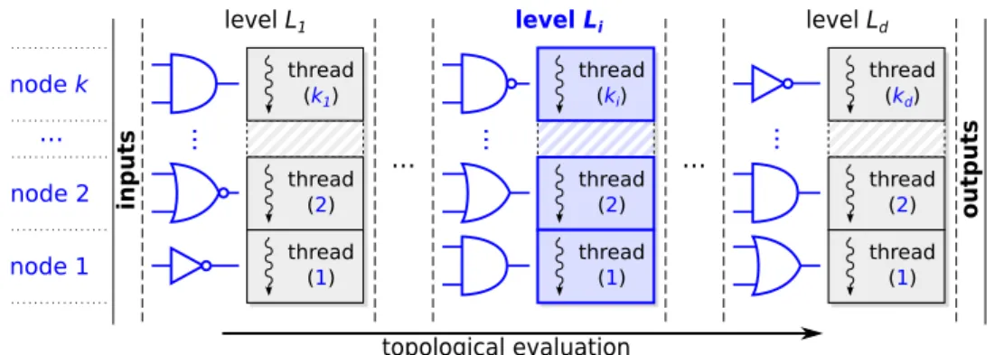
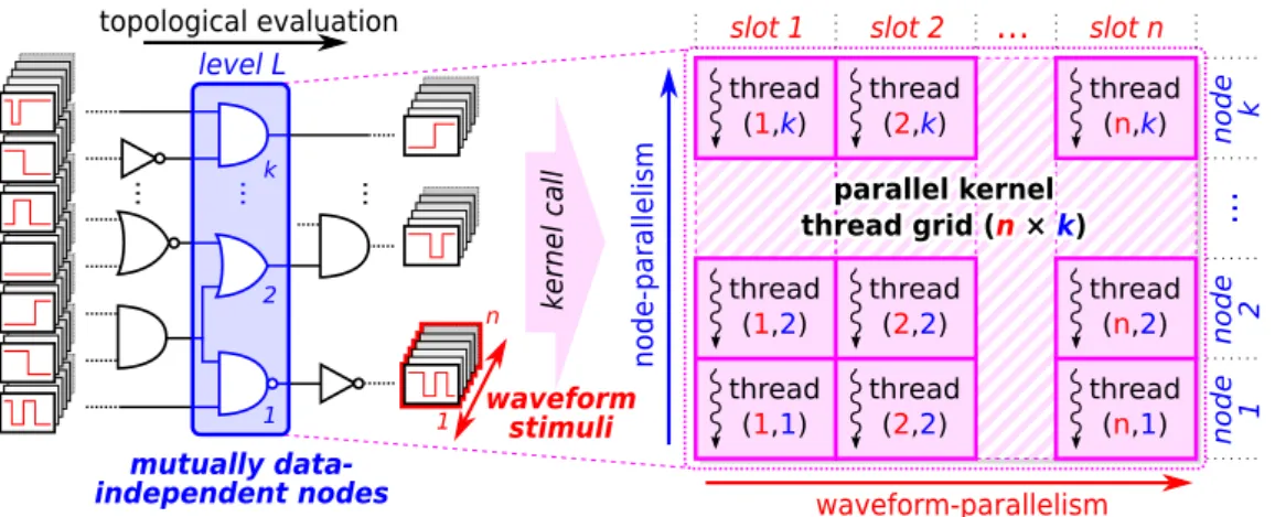
5.6 Structural and Data-Parallelism . . . 75
5.7 Thread Organization for Structural Parallelism . . . 76
5.8 Two-dimensional Thread Organization . . . 77
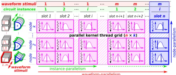
5.9 Multi-dimensional Thread Organization with Instance Parallelism . . . 78
5.12 Memory Reduction . . . 84
5.13 Overall Simulation Flow . . . 87
5.14 Parallel Pattern-to-Waveform Conversion . . . 90
5.15 Parallel Waveform-to-Pattern Conversion . . . 91
6.1 Pattern-dependent Delays due to Multiple-Input Switching . . . 94
6.2 Extraction of Channel-Connected Components . . . 96
6.3 Resistor-Resistor-Capacitor (RRC-) Cell Model . . . 97
6.4 Curve-Fitting of Transient Responses . . . 102
6.5 Switch Level Event Representation and Visualization . . . 102
6.6 Switch Level Waveforms of a two-input NOR-Cell . . . 106
6.7 Time-continuous Simulation State of the NOR-Cell Example . . . 110
7.1 Fault Simulation Flow . . . 116
7.2 Mapping of Small Delay Faults at Outputs to Input-descriptions . . . 118
7.3 Greedy Fault Grouping Heuristic . . . 130
7.4 Fault Grouping Example . . . 132
7.5 Parallel Syndrome Calculation . . . 133
8.1 State Transitions in ternary Logic Waveforms . . . 140
8.2 Ternary Logic Waveform Example . . . 140
8.3 Multi-Level Simulation Flow . . . 141
8.4 Multi-Level Waveform Transformation: Logic-to-Switch Level . . . 146
8.5 Multi-Level Waveform Transformation: Switch-to-Logic Level . . . 148
8.6 Generic Multi-Level Node Description . . . 148
8.7 Node Expansion and Collapsing . . . 151
8.8 Generic Waveform Structure . . . 151
8.9 Transparent Parallelization of the Multi-Level Simulation . . . 152
10.1 Logic Level Simulation Performance Trend . . . 165
10.2 Logic Level Simulation GPU-Device Exploration . . . 165
10.4 Switch Level Simulation GPU-Device Exploration . . . 169
10.5 Multiple Input Switching in a NAND3_X1 Cell . . . 170
10.6 Pattern-dependent Delay Test Circuit . . . 171
10.7 Waveforms of Electrical, Logic and Switch Level Simulation in Comparison . 172 11.1 Resistive Open-Transistor Fault Simulation Results . . . 182
11.2 Resistive Open-Transistor Fault Behavior . . . 184
11.3 Capacitive Fault Simulation Results . . . 185
11.4 Capacitive Fault Behavior . . . 186
12.1 Switching Activity Characterization at Logic Level . . . 189
12.2 Weighted Switching Activity Comparison . . . 190
12.3 Distribution of Switching Activity in Time-Slices . . . 190
12.4 Clock-Skew in the Clock Tree . . . 192
12.5 Correlation of Skew Estimates for Circuit b14 . . . 193
12.6 Correlation of Skew Estimates for Circuit b18 . . . 194
13.1 Multi-Level Simulation Performance . . . 196
13.2 Multi-Level Simulation Speedup . . . 198
13.3 Runtime Savings of Mixed-Abstraction Simulation . . . 199
List of Tables
6.1 Switch Level Event Table Example . . . 108
6.2 Switch Level Device Table Example . . . 108
9.1 Specifications of the used GPU Devices . . . 156
9.2 Number Symbols and represented Order of Magnitude . . . 158
10.1 Logic Level Simulation Performance . . . 163
10.2 Switch Level Simulation Performance . . . 168
11.1 Fault Collapsing and Fault Grouping Statistics . . . 177
11.2 Fault Detection of Transition and Small Delay Faults . . . 178
11.3 Random Process Variation Impact on Small Delay Fault Detection . . . 181
A.1 Benchmark Circuits and Test Set Statistics . . . 228
B.1 Characterization of Switching Activity at Logic Level . . . 230
B.2 Weighted Switching Activity of timed and untimed Simulation . . . 231
B.3 Resisitive Open-Transistor Fault Simulation Results . . . 232
B.4 Capacitive Fault Simulation Results . . . 233
List of Abbreviations
ATPG Automatic test pattern generation
CAT Cell-aware test
CCC Channel-connected component
CLF conditional line flip
CMOS Complementary metal-oxide semiconductor
CUDA Computer unified device architecture
DSPF Detailed parasitics file format
EDA Electronic design automation
ELF Early-life failures
EM Electro-migration
FAST Faster-than-at-speed test
FinFET Fin-type field-effect-transistor
FLOP Floating-point operation
GND Ground voltage potential
GPU Graphics processing unit
HCI Hot-carrier injection
IFA Inductive fault analysis
MEPS Million (node) evaluations per second
MIS Multiple-input switching
NBTI Negative-bias temperature instability
PPSFP Parallel-pattern single fault propagation (fault simulation)
ROI Region of interest
RTL Register-transfer level
SDF Standard delay format
SM Streaming multi-processor
SPICE Simulation program with integrated circuit emphasis
STA Static timing analysis
STF slow-to-fall
STR slow-to-rise
TDDB Time-dependent dielectric breakdown
Chapter 1
Introduction
In modern semi-conductor development cycles of nanometer CMOS integrated circuits, the simulation of circuits is one of the most important and complex tasks for design and test validation. Circuit simulation is used for design validation to analyze developed de-signs with respect to validation targets to indicate the compliance with their specification or customer requirements. In test validation on the other hand, fault simulation is utilized to evaluate the defect coverage of test sets and new test strategies, as well as to assess the quality of the tested products. For this, electronic design automation(EDA) tools for design and test validation have to rely on repeated, compute-intensive circuit simulations with extensive runtimes, which can pose a bottleneck, especially for designs with billions of transistors [ITR15].
Simulation itself is best described as"performing experiments on a model"of the real (phys-ical) world [Cel91, CK06]. The models for simulation typically provide a set of properties and rules, that represents and explains parts of the complex real world behavior in an abstract manner. Once an algorithm has been derived from the model, a simulation pro-gram(simulator) can be efficiently utilized to perform and observe experiments repeatedly on the model for any given input parameters. The output of the simulation then provides data that can help to make predictions regarding the real world behavior. This way, knowl-edge can be obtained to validate real world hypotheses without the need of costly (and often destructive) experiments in the real world.
For example, in circuit simulation abstract models of the real physical silicon chips are provided, that allow to run experiments to predict and observe the behavior of prototype
designsand compare it to its specification. The designer can then draw conclusions from the results to assess the provided functionality of the prototype design, the correctness as well as other non-functional aspects (i.e., timing reliability, power) [WH11, Wun91]. Fault simulation is an extension of circuit simulation in which the behavior of arbitrary defects in a real physical chip are abstracted to faults. Each fault describes the altered chip behavior with respect to a given defect mechanism, which is reflected as abstract deterministic misbehavior in the underlying circuit simulation model.
The abstraction of a simulation model itself is crucial to avoid dealing with the overall complexity of the real physical world and to make an evaluation feasible at all. While a high accuracy of a simulation model is generally desirable, it can make simulations infeasible due to a high time- and space complexity of the evaluations. By constraining the model to certain aspects and by using simplified assumptions, the costs of the simulations can be lowered and evaluation can be focused on certain problems of interest. On the other hand, too much abstraction reduces the accuracy of the models and also the viability of the simulation and its results.
Challenges
With the continuing advancements in semiconductor manufacturing processes and shrink-ing technologies of digital integrated CMOS circuits, traditional circuit and fault simula-tion models have become insufficient. Nowadays, thorough design and test validasimula-tion as well as diagnosis require more and moreaccurate simulations and have thus become complex and runtime-intensive tasks, since several aspects have lead to an increase in the overall modeling and simulation effort:
Complexity of Circuit Size
Over the past decades, semiconductor manufacturing technologies and processes made continuous advancements that still allow for an ongoing growth in complexity and higher integration of modern integrated circuits [ITR15]. Although Moore’s Law [Moo65, Moo75] was already predicted to end [RS11], newer process technologies, such as thefin-type field effect transistor (FinFET), enable a scaling of structure sizes down to a few nanometers
only and the production with higher transistor density [Kin05, Hu11]. For example, in 2017 NVIDIA announced a new generation of parallel GPU accelerators: The NVIDIAR
VoltaTM architecture. The GV100 GPU chip of the family is manufactured in a 12nm
FinFET technology and comprises 21.1 billion transistors on a die of 815 mm2 in size [NVI17d]. To validate such massive designs, scalable parallel simulation algorithms are required that are able to cope with the increasing design complexity and its millions or billions of transistors.
Complexity of Circuit Behavior
While technology scaling causes the circuits to grow in size and functionality, the be-havior of standard cells and circuit structures is becoming more and more complex as well [ITR15]. With the increasing demand for high-performance and low-power em-bedded designs, chips are running today at their operational limit [SBJ+03, DWB+10,
KET16, GKET16]. Furthermore, the circuit structures become more and more prone to process- [ZHHO04, QS10] and parameter variations (e.g., voltage and temperature [BPSB00, BKN+03, TKD+07]), which can impact the reliability of the circuit and
effec-tiveness of tests if neglegted [PBH+11, HBH+10, CIJ+12]. Therefore, accurate simulation
models are required that deliver sufficiently high precision and detail to capture both functional as well as non-functional aspects of the circuit with as little abstraction as pos-sible. The circuit models must provide support for accurate representation of the temporal behavior to reflect hazards and glitches, signal slopes and parametric and parasitic depen-dencies. Also, pattern-dependent delays and multiple-input switching effects should be considered as they can significantly alter the circuit delay [MRD92, SDC94, CS96]. How-ever, such timing-accurate evaluations involve the vast processing of many real numbers through complex arithmetic operations, which is several times more expensive in term of computing complexity compared to untimed logic simulation [SJN94] and also much harder to parallelize [BMC96].
Complexity of Defect Modeling
The complexity of a simulation quickly rises further as soon as the behavior of defects in a circuit needs to be investigated in fault simulation. While classical fault models and
simulation approaches have been extensively studied and optimized in the past [Wun10, Wun91, WLRI87], modern semiconductor manufacturing processes have to deal with several new fine-grained types of defects [LX12, RAH+14, HRG+14, ITR15]. Small
de-lay defects (SDD) [TPC11, RMdGV02], marginal devices [RAH+14, KCK+10, KKK+10]
andwear-out-related effects due to circuitaging [LGS09, APZM07, BM09, GSR+14]
im-pact the timing behavior of the circuit and require timing- and glitch-accurate evaluation [Kon00, YS04, HS14], especially when considering process variations on top [PBH+11,
HBH+10, CIJ+12]. While certain validation tasks can utilize formal verification
meth-ods [DG05], the modeling and evaluation of low-level faults and parameters in explicit simulation is much more intuitive and straight-forward [Lam05], especially when a vali-dated formal model does not exist.
Moreover, the faulty behavior of many realistic defects often cannot be represented at higher abstraction levels as their behavior strongly depends on the physical layout as well as the low-level topology and technology of the standard cells [SMF85, FS88]. For this, cell-aware test(CAT) approaches have been recently developed [HRG+14] that
ex-tensively rely on expensive low-level analog fault simulations withuser-defined fault mod-els (UDFM). Thus, it is important to efficiently simulate faults with little abstraction as accurately and efficiently as possible [CCCW16].
Parallelism as a Remedy
Assume that a circuit ofN nodes with a setFof faults needs to be simulated for a pattern setT under different operating parametersP. In a naïve flow, a total ofN× |F | × |T | × |P| individualsimulation problems have to be solved, each of which corresponds to complex arithmetic evaluations of the timing behavior at a node. Thus, with growing design size, the number ofsimulation problemsquickly rises since the number of nodes, faults and test patterns also increase.
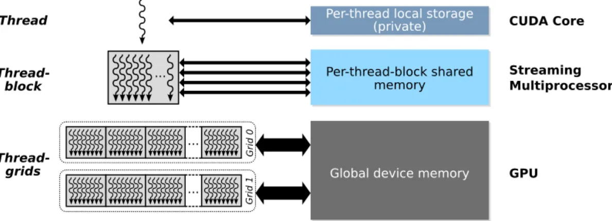
Although circuit- and fault simulation are inherently parallelizable [IT88, BBC94, BMC96], the parallelization has risen to a whole new level with the introduction of general purpose computing ongraphics processing unit(GPU) accelerators [OHL+08]. In contrast to
GPU-architectures provide thousands of compute cores on a single device for running millions of threads concurrently [NVI17d]. With this amount of compute cores, the GPU-based sys-tems attain unprecedented arithmetic computing throughput in the order of petaFLOPS1
on a single compute node, which has established well in high-performance computing for speeding up many applications [NVI18c].
Many approaches that parallelize logic level simulation on GPUs for acceleration were published [GK08, Den10, KSWZ10, CKG13, WLHW14, LTL18] that isolate and partition the simulation problems for independent parallel execution by individual threads, but only very few are able to consider actual timing. Analog simulation with GPU-support [GCKS09, CRWY15, CUS19] and full GPU-accelerated SPICE implementations [HZF13, HF16, vSAH18] have been proposed as well. However, existing parallel approaches for either logic level or analog simulation are mainly optimized for speeding up single simu-lation instances only. Since the number of simusimu-lation problems is continuing to rise, it is of utmost importance that the approaches are not only efficiently parallelizable, but also scalableby providing high-simulation throughput to make an evaluation of large designs for more complex algorithms feasible.
Timing Modeling at Logic Level
For the calculation of the full signal switching histories in a circuit, traditionalunit delay models [Wun91] have become insufficient. Instead, timing-accurate simulation models are required that are able to process real-valued gate delays for individual gate pins and signal switches [IEE01a]. Since the execution of bare arithmetic floating-point instructions has much higher latency compared to bit-wise logic operations of traditional untimed logic simulation, timing-accurate simulation of a million-gate circuit for a test pattern set can take hours or even days to complete [SHK+15].
On GPUs, long-latency processes and arithmetic operations can be hiddenby the massive computing throughput provided by the parallel computing cores [OHL+08]. For this,
massive parallelization needs to be exploited to effectively speed up extensive logic level simulations with timing-accurate and variation-aware delay models for large designs and test sets.
Switch Level Modeling and Algorithms
Timing-accurate and lower-level models are desirable for accurate simulation of digital integrated CMOS circuits. While simulation at logic level lacks accuracy, SPICE simulation lacks scalability even when accelerated by parallelization. As a trade-off, switch level simulation was introduced [Bry87, Hay87, BBH+88, MV91] which drastically reduces the
complexity of the evaluation compared to full analog simulation. While not being as accurate, switch level modeling reflects many properties of CMOS circuits and standard cells that cannot be modeled at logic level. This has recently drawn attention incell-aware test(CAT) generation to reduce the analog fault simulation overhead [CCCW16, CWC17]. Yet, the simulation at switch level is still an order of magnitude slower compared to logic simulation [SJN94] and therefore poses a strong bottleneck in validation tasks, which makes it a prime-example for the acceleration on GPUs. However, to the best of the author’s knowledge no algorithms to accelerate switch level simulations on GPUs exist.
Defect Modeling and Fault Simulation
Many defects types exhibit a varying faulty behavior based on thesizeor magnitude of the defect parameter. The behavior of such a parametric defect can range from a hard func-tional failure of the circuit, to aweakimpact on the non-functional timing behavior that only affects the circuit performance [RMdGV02, FGRC17]. With the continuously shrink-ing circuit structures, the probability of such defects as well as their severity with respect to the circuit reliability rises [ITR15], while at the same time the faults are becoming harder to detect [LX12, TTC+15]. Thus, thorough test validation requires a fine-grained
model-ing of the defect parameters to capture deviations in both functional and non-functional aspects of the circuit (e.g., small delays [YS04, LKW17, KKL+18]).
To reflect the behavior of more realistic defects found in CMOS cells, faults must be modeled at the lower levels without introducing too much abstraction [FS88, CCCW16, CWC17]. This vastly increases the computational overhead, as the defect mechanisms not only get more complex, but also many simulations of different individual faults are necessary (e.g., for fault coverage estimation). Thus, the need for parallelization of fault simulation is unavoidable [IT88, Wun91]. With their large amount of parallel arithmetic
compute cores, GPUs provide high arithmetic computing throughput that is promising to simulate even large designs for many faults and test patterns with full timing-accuracy.
Multi-Level Simulation
The modeling and simulation at higher abstraction is fast, but the approaches are limited in accuracy such that often timing and defects cannot be reflected properly [RAH+14].
On the other hand, lower level approaches can provide sufficient accuracy, but exhibit significant runtime complexity and resource requirements, such that the approaches can-not be used solely for a system-wide application (i.e., system-level test validation [Che18, JRW14]). However, advantages from both higher- and lower-level abstractions can still be taken into account at the same time by usingmulti-leveltechniques.
Amulti-levelsimulation provides a combined simulation across multiple different levels of abstractions [GMS88, MC95, RK08, KZB+10, HBPW14]. Accurate and compute-intensive
evaluations are typically restricted to a particular region of the circuit [HBPW14, KZB+10],
or single cells [CCCW16], whereas the remainder is processed using faster higher-level simulations. Intermediate simulation data is usually exchanged at abstraction boundaries by data aggregation and mapping to the respective higher- or lower-level inputs [JAC+13,
HBPW14, CCCW16]. Thus, compared to full simulations at the lowest abstraction, multi-level simulations can provide a trade-off in terms of speed and accuracy and make certain simulation scenarios even feasible at all [JAC+13, HKBG+09, CCCW16].
Applications
High-throughput timing-accurate circuit- and fault simulation is helpful to accelerate ap-plications in a variety of areas, which heavily rely on extensive simulations.
Process variability and timing variation: With the increasing sensitivity of circuits to-wards process- and parameter variation, the need for statistical evaluations for perfor-mance and reliability assessment rises. Under variation, the circuit timing is severely altered [BCSS08, GK09] which tampers with the effectiveness of tests [PBH+11]. By
in-cluding parameter dependencies in the delay processing, such as supply voltage and am-bient temperature [DJA+08, SAKF08], or process variations [ABZ03, ZHHO04], statistical
timing analyses [WW13] and statistical fault coverage analysis [SHM+05, CIJ+12] can be
realized by large-scale Monte-Carlo evaluations in highly parallel timing simulation.
Non-functional properties: The timing-accurate switching histories from the simula-tion can be utilized to analyze non-functional properties in a design. Both, thermal de-sign power [HGV+06] and IR-drop from switching activity hotspots [SBJ+03, MSB+15,
DED17a] impact the reliability of designs and tests [WYM+05, ZWH+18] and thus need
to be evaluated. Moreover, vulnerabilities with respect to single-event upsets [BKK+93]
and aging effects, such asbias temperature instability(BTI) [GSR+14] orhot-carrier
injec-tion(HCI) [LGS09, ZKS+15], can be investigated using timing-accurate signal histories.
Power estimation: The static and dynamic power-consumption of a design can be es-timated from the circuit signals and switching activity [GNW10]. Power consumption tampers with the functionality of the design not only during functional operation, but also during the application of tests [WYM+05, AWH+15]. While previous approaches
relied on untimed logic simulation due to complexity reasons, the power of GPUs en-able timing-accurate power estimation for many patterns in parallel. This way more-accurate power-aware test schemes and test pattern selection can be developed [HSW+16,
HSK+17, ZWH+18].
Scan test: Timing-accurate simulation is necessary to validate delay tests for small delay defects and marginalities, i.e.,faster than at-speed test(FAST) [HIK+14, KKL+18].
How-ever, in scan test each test pattern undergoes a long session of consecutive shift cycles before the test can actually be applied and evaluation [GNW10]. During the shift-phase, IR-drop-induced shift-errors from delayed signals [YWK+11] as well as skewed clocks
[Sho86] can cause errors during shift-in and shift-out phases of the test pattern applica-tion. Again, with the high-throughput computing capabilities of GPUs, parallelization can be utilized to accurately evaluate full test sets with millions of shift cycles concurrently.
Goal of this Thesis and Organization
The document at hand presents highly parallel simulation models and simulation algo-rithms for fast and scalable timing simulation of nano-electronic digital integrated CMOS circuits ongraphics processing units(GPUs).
The main contributions of this thesis are summarized in Fig. 1.1. Compact functional as well as timing-accurate temporal modeling are combined with highly parallelized simula-tion algorithms designed to run on GPU-architectures to exploit their massive computing throughput. These building blocks provide the foundation for developing high-throughput simulation algorithms for timing-accurate logic level and switch level simulation with par-allel execution on the GPUs.
high-throughput parallelization compact
functional modeling
efficient high-throughput parallel timing & fault simulation of nano-electronic digital circuits
massively parallel graphics processing units (GPU) efficient simulation algorithms timing-accurate temporal abstraction [HSW12] [HIW15] [SHWW14]
small delay fault simulation [SHK+15]
[SKH+17] [SW16][SW19a]
multi-level timing & fault simulation [SW19b]
transistor level fault simulation logic level
timing simulation timing simulationswitch level [SKW18]
Figure 1.1: Contributions of this work.
The presented simulation models and algorithms are further extended for fault simula-tion of small delay faults at logic- as well as low-level parametric and parasitic faults at switch level. These allow to fully exploit the massive parallelism found in circuit and fault simulation on the GPU-architectures.
Finally, on top of these the extended simulation models and algorithms are ultimately combined to form an efficient multi-level fault simulation flow that enables additional sim-ulation throughput and simsim-ulation efficiency for the lower level fault simsim-ulation through the use of mixed abstractions during simulation.
By simultaneously exploiting different dimensions of simulation parallelism, the presented parallel simulation techniques achieve unprecedented simulation throughput on GPUs
thereby enabling scalable timing and fault simulation of multi-million gate designs, which effectively reduces simulation time from several hours or even days to minutes only. The structure of this document is organized into three parts:
The first part (Chapter 2–4) introduces background on circuit- and fault modeling as well as simulation. Furthermore, the part briefly summarizes the key aspects of data-parallel many-core computing architecture ofgraphics processing units(GPU) and their program-ming paradigm, along with an overview of state-of-the-art GPU-accelerated simulation techniques.
The second part of this document handles the high-throughput time- and fault simulation, which is the main contribution of the thesis and is composed of the following chapters:
Chapter 5 (”Parallel Logic Level Time Simulation on GPUs”) – presents the first timing-accurate and variation-aware logic level time simulation on GPUs and outlines the underlying algorithms, kernels and general data structures for multi-dimensional parallelization with high simulation throughput.
Chapter 6 (”Parallel Switch Level Time Simulation on GPUs”) – introduces the first parallel switch level time simulation for GPUs which utilizes first-order electrical parameters found in CMOS circuits for a more accurate modeling of the functional and timing behavior of CMOS standard cells.
Chapter 7 (”Waveform-Accurate Fault Simulation on GPUs”) – describes the extension of the logic- and switch level simulation algorithm for fault modeling, syndrome com-putation and parallelization for first-time detailed and comprehensive parallel sim-ulation of timing-related faults.
Chapter 8 (”Multi-Level Simulation on GPUs”) – addresses a combination of the presented parallel logic- and switch level algorithms in the first GPU-accelerated multi-level simulator that effectively enhances the performance and efficiency of the lower-level timing and fault simulation.
The third and last part (Chapter 9–13) discusses the evaluation of the aforementioned presented simulation methodologies as well as example applications in five chapters. Finally, the last chapter provides a summary of all the contributions of this thesis and outlines directions for future work and possible extensions.
Part I
Background
Chapter 2
Fundamental Background
This chapter summarizes the necessary background and fundamentals of circuit- and fault modeling as well as simulation of digital integrated CMOS circuits as found in basic litera-ture [Wun91, BA04, WWX06, WH11]. First, background on standard CMOS technology is provided, followed by circuit- and delay fault modeling on different levels of abstraction. Finally, simulation algorithms and multi-level simulation methods are briefly discussed.
2.1
CMOS Digital Circuits
Today’s semiconductor manufacturing processes of digital integrated circuits mainly rely on complementary metal-oxide semiconductor (CMOS) technology. CMOS uses two types of metal-oxide-semiconductor field-effect transistor(MOSFET) devices, namely NMOS and PMOS transistors, that can basically be considered as voltage-controlled switches. NMOS and PMOS transistors are utilized to formstandard cellsinstandard cell libraries[Nan10, Syn11] which are the foundation of contemporary semiconductor design. For more details on the structure and mechanics of transistors as well as the manufacturing processes and design of standard cells, the reader is referred to [WH11].
In modern semiconductor process technology nodes, conventional planar MOSFETs are being replaced by the recentfin-type field-effect transistor(FinFET) technology [HLK+00,
Kin05, BC13]. The FinFET devices allow for scalable manufacturing of feature sizes be-yond 20nm, since they have a more compact layout with a faster switching behavior com-pared to traditional transistors [YMO15]. This enables the production of more complex
designs with higher transistor density that can be further run at higher clock frequencies to achieve even higher device performance. Although the physical structure of planar MOS-FET and FinMOS-FET is different, their basic working principles and design flows are similar.
2.1.1 CMOS Switching and Time Behavior
In today’s nanometer regime, it is often of utmost importance that the designs meet a certain performance requirement that is given by a minimum system clock frequency. The highest frequency a design can reliably run with is usually determined by the length of the critical path. The critical path accumulates all the propagation delays of standard cells and interconnects on the longest sensitizable path from a primary or pseudo-primary input to a primary or pseudo-primary output in the design.
In general, the delays of a standard cell are distinguished bypropagation delaysand rise/-fall timesas shown in Fig. 2.1, which depicts the typical input and output waveform of a inverter cell in a small circuit (15nm FinFET technology [Nan14, BD15] powered with a supply voltage of 0.8V). The maximum signal amplitude on the left axis has been normal-ized. As shown, the signal switching processes do not occur instantly, but occur merely as a function of the voltage over time as a result of parametric and parasitic electrical elements in the circuit. The change of the voltage of a signal is typically modeled by differential equations that describe electrical charging and discharging processes of capacitances in the circuit [WH11]. 0 0.5 1 0 10 20 30 40 50 Signal [V] (normalized) time [ps] input output dr df dlh dhl 80% 20%
Figure 2.1: Rising/falling propagation delay (dr,df) and rise/fall timesor slopes(dlh,dhl)
of an INV_X1 CMOS inverter cell [Nan14, BD15]. (Adapted from [WH11])
Thepropagation delayis defined forrising(low-to-high) andfalling(high-to-low) output transition polarities (dr anddf) and describes the time it takes for a signal transition at
a cell input to propagate to the cell output. It is measured from the time point where the input signal reaches the 50% mark of the maximum signal amplitude (i.e.,0.5·VDD
2.1 CMOS Digital Circuits
as halfway between VDD and GND potential) to the point where the output crosses 50% of the maximum signal amplitude in response [WH11]. Moreover, as shown in Fig. 2.1, signal transitions are not instantaneous, but follow a certain continuoustransition rampor slopethat are given by therise-timedlh forrisingand thefall-timedhlforfallingtransitions
as well. The rise-time (and fall time) of a signal transition is defined as the time it takes to transition from 20% to 80% of the maximum signal amplitude (and vice versa), though these thresholds can vary throughout the literature (e.g., 10%–90%) [WH11].
With the shrinking manufacturing process technologies and increasing complexity, it is important to accurately estimate the possible timing of contemporary and future designs. Thus, suitable models are required to reflect and consider CMOS-related timing effects as early and as accurately as possible during the design phase.
One approach to estimate the delay of a circuit is the RC delay model [WH11], which approximates the non-linear characteristics of transistors considering average resistances and capacitances of the circuit nodes. In the RC delay model, the circuit netlist is trans-formed into an electrical equivalent RC-circuit where all transistors and interconnects are replaced by simple resistors and the interconnect- and gate capacitances in the fanouts are replaced by (in the simplest case) lumped capacitances. A switching transistor causes a change in the state of the RC-model elements by changing the corresponding resistance. This triggers a transient at the output that is typically computed using the first-order or second-order step response [Elm48, WH11]. Hence, in case of the rising transient of Fig. 2.1 the step response vrise beginning at some time t0 can be modeled for the time
t > t0 after as
vrise(t) := (GND−VDD)·e −(t−t0)
τ +VDD, (2.1)
whereτ is thetime constantcomputed asτ :=R·C, withRbeing the effective resistance of the driving PMOS transistor andC being the load capacitance. The propagation delay
dr is then derived from the output signal vrise at the time it crosses 0.5·VDD, which is computed asdr :=τ·log 2[WH11]. Similarly, the falling transientvfall beginning at some timet1is calculated fort > t1 as
vfall(t) := (VDD−GND)·e −(t−t1)
in which case the resistanceRfor the time constantτ :=R·Ccorresponds to the effective resistance of the conducting NMOS transistor, resulting in an estimated falling propagation delay ofdf :=τ·log 2. Both of the modeled rising and falling transients expressed byvrise andvfall are illustrated in Fig. 2.2. The axes have been normalized byτ for the time and by VDD for the voltage, respectively. For the sake of simplicity, it was assumed that the internal resistances of NMOS and PMOS were equal.
0 1 0 1 2 3 4 5 Output [V] (normalized) time [τ] τ log 2 0.5 vvrise fall 80% 20%
Figure 2.2: First-order step response for rising and falling transient modeling the continu-ous charging/discharging process of an output load capacitance. (Adapted from [WH11].)
2.1.2 Circuit Performance and Reliability Issues
With the shrinking feature sizes in newer technologies, the semiconductor manufactur-ing processes get more complex and increasmanufactur-ingly prone to process variations and defects [SSB05, PBH+11]. Since the structures, such as fins of FinFET transistors, have a size
of only a few nanometers, spot-defects by particles or statistical processes in the different manufacturing steps, such as dopant fluctuations, are getting more and more frequent and influential. These problems can severely alter the physical layout of the circuit structures and lead to improper connections in the design. Moreover, transistor-related parameters, such as the threshold voltage and electron mobility, can shift due to improper manufactur-ing. The resulting defects, such as open and shorts in either fins or gates [LX12], as well as variation artifacts [HTZ15] primarily impact the timing of the circuit [TTC+15, FGRC17]
and ultimately affect the device performance and reliability by introducing delay faults. Certain parameter shifts in circuit structures exhibit small delays that sometimes indicate circuit agingor the presence of a marginal device [KCK+10]. For example, when a design is
put under stress (i.e., high switching activity or mechanical stress) after deployment, struc-tures in the circuit can fail due to device degradation and transistoraging[BM09]. These wear-out mechanisms appear gradually as a result of continuing static and dynamic stress
2.2 Circuit Modeling
in the circuit, i.e., by certain stimuli or circuit activity, as well as environmental conditions, such as temperature. Typical degradation mechanisms are Negative-Bias Temperature In-stability (NBTI) [LGS09, GBRC09], Hot-Carrier Injection (HCI) [EFB81, GSR+14],
Time-Dependent Dielectric Breakdown (TDDB) [DGB+98] and electromigration (EM) [Cle01].
The effects of the degradation range from changes in electrical properties of the transistor devices and interconnects [LQB08] that result in delay faults [BM09] up to hard fail-ures, such as voids or bridges due to transported metal atoms from EM. Imminent wear-out failures can be predicted using specialized hardware (e.g., aging monitors[APZM07, LSK+18]), once the circuit has sufficiently aged or degraded. Wear-out can also be
de-layed or mitigated by reducing the stress patterns in the circuit to prolong the system lifetime [ZBK+13].
Failures in the early-life phase of a design are related to infant mortality among circuits, where marginal devices have passed the conventional manufacturing test, but soon break after initial deployment. These failures are called early-life failures(ELFs). Marginal de-vices are usually tested using so-called Burn-In tests [VH99], that strongly exercise the circuit under extreme stress conditions to expose the ELF. The indicators of ELFs can be located deep inside the circuitry which can be barely noticeable as small delay devia-tions that are much smaller than the clock period and not testable under at-speed condi-tions [KCK+10]. This lead to the recent development of Faster-than-At-Speed Test(FAST)
[HIK+14, KKS+15] to explicitly test for these hidden delay faults (HDF) to identify the
marginal devices.
Therefore, to assess and validate the timing of today’s designs as well as to thoroughly test for timing-related defects, designers and testers have to rely on timing-accurate models of the circuits and simulation algorithms for test and diagnosis [TPC11].
2.2
Circuit Modeling
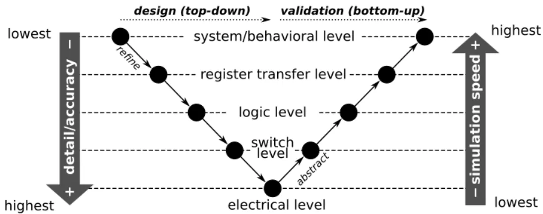
Today’s multi-billion transistor circuit designs are typically not manufactured starting from scratch using transistors, but rather starting from high-level specifications that describe its behavior in an abstract manner [Wun91]. As shown in Fig. 2.3, the circuit design undergoes different representations at various levels following a V-shaped model. During
the top-down design phase, abstract high-level descriptions are refined step by step by synthesis tools that systematically add more and more implementation details by mapping to lower level structures [ABF90, BA04, WWX06]. For example, at the highest level of abstraction, only the desired function is specified and the actual design itself is treated as a black box since no physical implementation details are present. At this level, modeling and simulation is fast and simple, but the accuracy is the lowest. When moving down towards the lower abstraction levels, the required gates to realize the specified function or even the layout of complete transistor netlists with physical and electrical properties are determined. This drastically increases the modeling complexity and, of course, the simulation effort, but ultimately leads to more accurate models and evaluations.
system/behavioral level register transfer level
logic level switch level electrical level design (top-down) re fine abstra ct validation (bottom-up) simu lat ion sp eed + − highest lowest detai l/ac cur acy + − lowest highest
Figure 2.3: Overview of abstraction levels of a circuit in the design and validation.
2.2.1 Electrical Level
The electrical level provides the highest accuracy among the commonly used simulation models as it reflects the physical properties and behavior based on layout. The circuit is modeled using netlists of electrical components and devices, such as transistor mod-els, resistors, capacitors, inductors and voltage sources. Corresponding simulators usually consider geometric information of the physical layout to reflect spatial dependencies of power-grid structures and capacitances between neighboring interconnection lines. Inter-nal node voltages and currents are typically calculated through compute-intensive nodal analyses and differential equations using numerical integration methods. This way, highly waveform-accurate transient analyses by electrical simulations can be provided which also allow to predict the signal integrity as well as the power consumption in a circuit [WH11].
2.2 Circuit Modeling
Modeling and simulation at the electrical level is typically performed using SPICE [NP73], which has established as industry golden standard. Common standard cell libraries [Nan10, Syn11] already provide SPICE models of the implemented standard cells, which utilize transistor device model cards that can include hundreds of parameters [DPA+17, Nan17].
However, the high detail and accuracy of the electrical level modeling comes at the cost of vast runtime complexity and memory requirements.
2.2.2 Switch Level
Switch level modeling abstracts the electrical level behavior of the circuit by simplification and linearization of the transistor switching behavior [Bry84, Bry87, Hay87, Kao92]. The circuit is represented as an interconnected network of transistors and first-order electrical components, i.e., resistors and capacitors, as shown in Fig. 2.4. Transistors are treated as simple three-terminal devices that form discrete ideal switches, where the input at the gate terminal controls the connection between drain and current terminal of the device. The resistors in the model reflect the static functional behavior, and the capacitors (sometimes referred to as wells) model the temporal behavior [Hay87]. Most switch level models distinguish between signal strengths and consider bi-directional signal flows as well as modeling of charges inside of the networks.
At switch level, signal values are typically represented as pairshs, viofsignal strengths∈
N andsignal valuev. The signal values are typically expressed internary (three-valued)
logic over the setE3 ={0,1, X}[Hay86, BAS97] to distinguish betweenlow(0),high(1)
and undefined(X) signals. Thesignal strength reflects the driving strength of the signal source, which is used to resolve multiple drivers at a node or consider bidirectional signal
A ZN VDD GND A ZN ⟨0,1⟩=VDD R C VA=GND vA=⟨0,0⟩ v1=⟨0,1⟩ v2=⟨0,0⟩ v3=⟨1,1⟩ ⟨0,0⟩=GND v4=⟨∞,0⟩ v5=⟨1,1⟩ vZN=⟨3,1⟩≈VDD VZN≈VDD A ZN vA=0 vZN=1 φNOT:ZN:=(¬A) "ON" "OFF" ∅
Figure 2.4: Inverter cell with CMOS implementation and switch level representation, where signal values are encoded as pairshsi, viiof strengthsiand logic valuevi[Hay87].
flows as well as stored charges in the network. Signals of strengths= 0are the strongest signals and typically correspond to VDD or GND sources, whereas higher values ofs indi-cate weaker signals. Stronger signal values always override weaker ones. Signals of the same strength, but with different values, result in anundefinedvalue.
For the purpose of efficient switch level simulation of digital designs, a common practice is to partition the transistor netlist of circuits and CMOS cells into smaller sub-networks composed ofidealPMOS and NMOS transistor meshes, forming achannel-connected com-ponent(CCC) [Bry87, DOR87, HVC97, BBH+88, BAS97, CCCW16]. The transistors within
a CCC are interconnected via their drain and source terminals to each other and connect power supplyVDD andgroundGND sources and allow for a bidirectional signal flow within the network. The outputs of a CCC are linked to an output domain that can lead to gate terminals of transistors in succeeding CCCs. However, it is assumed that no current can flow over the gate from one CCC into another.
Switch level evaluation algorithms are mainly based on nodal analyses and dependen-cies that are formulated using linear equations. These equations are solved using relax-ation techniques with sparse matrix vector products (SMVP) to first find a steady state solution of the node voltages and the node charges inside of the network after each in-put switch [Bry87]. In combination with timing analysis, node voltages are more ac-curately represented as a function of time, usually modeled by piece-wise approxima-tions [CGK75, Ter83, Kao92]. In general, switch level models are less accurate than elec-trical level models, but they are able to reflect many important properties of CMOS tech-nology which are not reflected in classical models based on two-valued Boolean or ternary pseudo-Boolean logic. Due to the higher speed of switch level simulation, it has replaced analog SPICE simulation in recent cell-aware test generation [CCCW16].
2.2.3 Logic Level
The logic level is the most dominant abstraction used in design and test validation of nano-electronic digital circuits [WWX06, BA04]. At logic level the circuit behavior is described asnetlistof interconnected Boolean gates. The netlist of a circuit is typically modeled as a directed graph G := (V, E). Each vertex v ∈ V corresponds to a node in the netlist, which corresponds to a Boolean gate, flip-flop, or circuit input or output, and basically
2.2 Circuit Modeling
represents a functional abstraction of a physical standard cell that determines the logical behavior. The edges (v, v0) ∈ E ⊆V ×V represent ideal interconnections from a source nodev∈V to a sink nodev0∈V in the netlist and allow for signal flows. Incoming edges at a node refer to input pins at the corresponding gate, while outgoing edges indicate the information transport from the node output pin to its successors.
Each edgee∈Eis associated with a signal value that reflects the logical interpretation of thevoltage levelof the corresponding signal, which are typically defined over two-valued Boolean logicB2 ={0,1}[Hay86]. The logic values in B2 correspond to discrete signal
states, where the logic symbol ’0’ corresponds tolowvoltage (i.e., ground voltage potential GND) and the symbol ’1’ corresponds to ahighvoltage (i.e., power supply voltage potential VDD). Multi-valued logic, such as ternary, four-valued, or even higher-order logic can be utilized to reflect additional states (e.g., unknowndue to uncertainties) and dynamic behavior (e.g., transitions) of signals [Hay86]. The functional behavior of a node withk
incoming edges is modeled by a Boolean function φ :B2k → B2 that maps the values of
the edges to an output value according to the function.
At logic level, various delay models can be considered to describe the temporal behavior of a gate output signal with respect to input changes. Apart from zero-delay modeling, which reflects the untimed simulation case, where input changes at time t can cause a simultaneous change at the output, timing-aware delay models evolve around unit-and multiple-delay representations to reflect propagation delays for gates (sometimes referred to as transport delays) [ABF90]. Fig. 2.5 provides an overview of the timing-aware delay models on the example of a small inverter gate [Wun91].
In unit delay it is assumed that all gates have a constant propagation delay d := 1 that corresponds to one time unit. For input transitions at time t ∈ N, this can cause output transitions to occur at timet0:= (t+d) = (t+1)in response. However, different gate types typically have different delays. Moreover, gates usually have different delays for rising and falling output transitions as well. Multiple-delaymodels reflect different transport delays
drforrisinganddf forfallingoutput transitions, which are applied accordingly.
Some delay models are able to consider propagation delays that are bounded by a min-max interval [dmin, dmax] ⊂ R [Wun91, BGA07]. In interval-based delay modeling, the
A ZN 1 2 3 4 5 6 0 time 0 1 0 1 ZN01 input signal unit delay (d=1) rise time dr=2, fall time df=1 ZN01 intervald min=1, dmax=2 7 8
ZN01 unit delay withinertial delay Δd<2 ZN01 unit delay withinertial delay Δd>2
A ZN
inverter gate
Figure 2.5: Overview of common (timing-aware) delay models in logic level simulation. (Adapted from [Wun91])
[dmin, dmax]. This way, process variations and uncertainties that impact gate delays can
be reflected. However, during simulation with such a model the uncertainty of different gates can quickly accumulate and lead to pessimistic simulation results [ABF90].
When the value at a gate output switches, the load capacitance associated with the stan-dard cell implementation at the electrical level is (dis-) charged, which requires some time until the transition is finished. In case a pulse at a gate input is too short, the output does not have sufficient time to charge to the targeted potential, which can prevent the propa-gation of the pulse, such that the output value is sustained. A so-calledinertial delaycan describe theminimum pulse width ∆d∈Rrequired to perform a full (dis-) charge of the output. For example, in Fig. 2.5, signal A has two consecutive pulses at timest1 := 1and
t2 := 3, which would lead to transitions at timest01 := 2andt02 := 3under unit delay. In
the last case, the required minimum pulse width is∆d >2, therefore the pulse is filtered out since the pulse width given by(t02−t01) = 2does not meet the requirement.
Individual delays for each input pin of a gate can be considered in combination with rising and falling distinction. So-calledpin-to-pindelay models keep a delay value di for each input piniof a gate. An input transition at pin iat timetthen propagates to the output at timet0 := (t+di)with the corresponding delay associated to the pin.
The logic level timing information is usually provided asstandard delay format(SDF) files [IEE01a] which are obtained during the synthesis of the design. Each SDF file typically contain absolute and incremental delay specifications describing, specific delays for indi-vidual ports (PORT), the propagation delay from an input to an output pin (IOPATH) as
2.3 Delay Faults
well as wire delays (INTERCONNECT) between gate instances. In addition to the
propaga-tion delays, inertial delays can be specified (via PULSEPATH) that describe the minimum allowed pulse-widths at outputs for the application of pulse filtering [IEE01a, IEE01b].
2.2.4 Register-Transfer Level
At theregister-transfer-level(RTL) the circuit module descriptions are mapped to a coarser structural description composed of small interconnected components [Wun91]. The com-ponents can be registers or memory to store data and operands, and combinational net-works to perform operations. Interconnections and buses define the data-flow between the individual components. The data exchange between memory elements is controlled in a synchronized fashion by clock signals. RTL-descriptions are typically expressed as data-flow in hardware-description languages, such as Verilog [IEE01b] or VHDL [IEE09]. While timing can be expressed in cycle granularity, fine-grained propagation delays are not considered at this level, since no implementation details are available.
2.2.5 System-/Behavioral Level
Atsystem level the circuits are modeled with the highest abstraction. Abstract functional descriptions of circuit modules are typically expressed as algorithms and functions in higher level programming languages, such as SystemC [IEE12], which are compiled and run as separate processes. Since no details or requirements with respect to the actual im-plementation of the design is implied, a reasoning about accurate timing is not possible.
2.3
Delay Faults
In test validation and diagnosis,fault modelsare used which abstract the effect of classes of physical defects in a chip for representation and processing on a higher abstraction level [Wun91]. As opposed to classical static fault models, such as stuck-at and bridging faults, a circuit cannot be tested for delay faults by using a single test pattern only [WLRI87]. Instead, delay tests with a minimum of two patterns composed of an initialization and propagation test vectorare required. These patterns are applied in consecutive clock cycles to launch signal transitions at (pseudo-)primary inputs. The output responses are then
captured after the clock period has passed, which might reveal output signals that are not yet stabilized.
A generalized way to model arbitrary faults in logic simulation is the so-calledconditional line flip (CLF) calculus [Wun10]. Each CLF has an activation condition cond, which is an arbitrary user-defined Boolean formula to determine the activation of the fault at a signalv. Once a CLF is active (conditioncond istrue), it flips (inverts) the value ofv to
v0 :=v⊕[cond]. As a simple example: A stuck-at-0 fault is represented in the CLF calculus asv⊕[v]and a stuck-at-1 fault is represented asv⊕[v].
Transition Faults
Thetransition fault model [WLRI87] assumes a lumped defect at a gate input or output pin that causes a delay at the associated signal line by an amount of time larger than the test clock period (usually infinite), thereby omitting a transition. Transition faults can be distinguished as slow-to-rise (STR) or slow-to-fall (STF) faults that affect rising and fallingtransition polarities, respectively. They are usually considered as conditional stuck-atfaults, which can be efficiently implemented and simulated using parallel-pattern stuck-at fault simulation by activating the fault upon signal changes of subsequent patterns [Wun10, WLRI87]. Therefore, regarding the modeling and simulation, transition faults are independent of the actual circuit timing and gate delays.
For example, letvi ∈B2 be the value at a signal line after application of the initialization
vector, and letvi+1 ∈B2 be the value after the subsequent propagation vector. The fault
activation at a signal line transitioning fromvi tovi+1 upon the clock cycle is determined
byactive ⇔(vi⊕vi+1)·ρ, where the term(vi⊕vi+1)indicates a change in the signal value
andρdetermines the activation of a STR (ρ:=vi+1) or STF (ρ:=vi+1) fault, respectively.
Note that transition faults always affect all sensitized paths in the output cone of the fault site regardless of the actual timing. Therefore, the fault model fails to accurately represent delay faults of smaller quantities, e.g., small resistive open defects.
Path-Delay Faults
Thepath-delay faultmodel [Smi85] was proposed to model distributed delay effects in the circuit and assumes the accumulation of smaller lumped delays during signal propagation.
![Figure 5.4: Logic level waveforms (B 2 ) of signals A and B before and after passing through NAND and XOR nodes with a delay of 1 time unit [HSW12].](https://thumb-us.123doks.com/thumbv2/123dok_us/10222976.2926177/91.892.168.681.105.433/figure-logic-level-waveforms-signals-passing-nand-nodes.webp)
![Figure 5.6: Two-dimensional evaluation by utilizing structural parallelism from nodes and data-parallelism from waveforms [HSW12, HIW15].](https://thumb-us.123doks.com/thumbv2/123dok_us/10222976.2926177/97.892.207.645.106.289/figure-dimensional-evaluation-utilizing-structural-parallelism-parallelism-waveforms.webp)