Iranian Journal of Electrical and Electronic Engineering, Vol. 15, No. 4, December 2019 502
Electrical μ-Lens Synthesis Using Dual-Junction
Single-Photon Avalanche Diode
S. Ejdehakosh* and M. A. Karami*(C.A.)
Abstract: This work presents a dual-junction, single-photon avalanche diode (SPAD) with electrical μ-lens designed and simulated in 90 nm standard complementary metal oxide semiconductor (CMOS) technology. The evaluated structure can collect the photons impinging beneath the pixel guard ring, as well as the pixel active area. The fill factor of the SPAD increases from 12.5% to 42% in comparison with similar works on the same technology, according to new charge collections. Although the designed SPAD suffers from high dark count rate (DCR of 300kHz at 0.17V excess bias at room temperature) due to high amount of tunneling which was predicted in previous similar works, it still can be used in different applications such as random number generators and charged particle positioning pixels.
Keywords: SPAD, μ-Lens, CMOS, Fill Factor, PDP, DCR.
1 Introduction1
INGLE photon avalanche diode (SPAD) is a semiconductor p-n junction based, solid-state single photon detector, biased above the breakdown voltage (Geiger mode) to generate an avalanche by photon absorption. In the Geiger mode of operation, the electric field strength in the depletion region should be above 3×10⁵ V/cm in Silicon[1]. Therefore, a
photo-generated carrier leads to a self-sustaining impact ionization and causes an electric current pulse in the output electrode of the diode. Hence, each pulse at the output electrode represents single photon detection. SPAD is widely used in range finding [2], fluorescence correlation spectroscopy (FSC) [3], fluorescence lifetime measurements [4], one[5] and two photon [6] fluorescence lifetime imaging microscopy (FLIM), 3D imaging [7], random number generation [8] and high speed imaging [9] . The main advantages of using SPADs are low power consumption, low bias voltage and compatibility with standard integrated circuits [10].
Iranian Journal of Electrical and Electronic Engineering, 2019. Paper first received 10 September 2018, revised 07 June 2019, and accepted 11 June 2019.
* The authors are with the School of Electrical Engineering, Iran University of Science and Technology (IUST), Tehran 1684613114, Iran.
E-mails: [email protected].
Corresponding Author: M. A. Karami.
The higher semiconductor impurity doping profiles which are used in deep submicron complementary metal oxide semiconductor (CMOS) technologies causes the reduction of the depletion region width and results in a decrease in the photon detection probability (PDP) [1]. The PDP is defined as the number of detected photons to the total number of impinging photons on the SPAD surface. On the other hand, considering thinner depletion region, band to band tunneling (BTBT) increases and leads to an increase in dark count rate (DCR) [11]. DCR is defined as the number of spurious detected pulses in the output without light illumination on SPAD surface [1]. SPADs are characterized by fill factor (FF), PDP and DCR. The fill factor is the ratio of photo-sensitive area to the whole pixel area [1].
While, optical μ- lenses are used conventionally to focus the light on the photo-sensitive active area of the pixel [12], fabrication of optical μ- lenses with low F-number (ratio of lens focal length to aperture) needs considerable technological efforts [13]. By expanding the photo-sensitive active area of the image sensor pixel, photons can be focused by the usage of high F-number optical μ-lens. This work presents the usage of electrical μ-lens as a replacement for low F-number optical μ-lens, where the pixel guard ring area is used for the light collection in SPAD. Conventionally the guard ring region is designed to engineer the electric field and the photons which are absorbed there cannot
S
Iranian Journal of Electrical and Electronic Engineering, Vol. 15, No. 4, December 2019 503 cause avalanche. For the same reason SPAD FF is
reduced in comparison with the other image sensors. The electrical μ-lens is working based on lateral avalanche propagation (LAP) [12]. In contrast to the optical lens which focuses the photons, in electrical μ-lens the electrons are the subject to be focused. In the SPAD presented in this work, the amount of electric field beneath the guard ring is high enough for SPAD to operate in Geiger mode, while the amount of electric field is simultaneously lower than the amount of electric field inside the active region. Hence an injected carrier beneath the guard ring depletion region leads to impact ionization and consequently, the electrons originated from the avalanche are guided to the SPAD center by LAP mechanism and can be collected at the output electrode. Therefore, the photons impinging beneath the guard ring can be counted deliberately. Furthermore, high F-number optical μ- lens itself can also be used to focus the photons.
This work presents a SPAD with electrical μ-lens designed in 90nm standard CMOS technology. A commercially available device simulator [14] is used to verify the simulations with the experimental results of [15].
Section 2 describes SPAD structure proposed in this paper. Section 3 describes the simulation results. Finally, the conclusions are given in Section 4.
2 SPAD Structure
A SPAD photosensitive region consists of two main parts of active region and guard ring, which the latter is used to prevent premature edge breakdown (PEB) formation. Various types of guard ring for PEB prevention in SPAD are used, such as: mesa isolation [16] field-limiting ring [17], diffused guard ring [18] and Shallow Trench Isolation (STI) [15]. STI is introduced in submicron CMOS technologies for crosstalk reduction, latch-up and punch-through prevention [1]. In this work simulation setup is formed based on the SPAD in [15], where the simulation was performed according to characteristics of 180 nm standard CMOS technology.
Fig. 1 shows the cross-section of SPAD presented in [15] where the p+/n-well interface is the
photo-sensitive active area and the STI is used as the guard ring.
The SPAD PDP in [15] is compared with the following analytical expression [15] in Fig. 2.
(1 ) A [1 exp( a)],
PDP RP F w (1)
In (1), R is the light reflectivity (ignored in [15]), ξ is the ratio of electron-hole pairs which does not recombine at the surface (surface recombination can drastically be reduced with using a surface passivation layer [19] ), PA is the probability that an electron-hole
pair lead to avalanche (which is simulated using model of [20] ), F is the fill factor, α is the absorption coefficient, and Wa is the multiplication region width
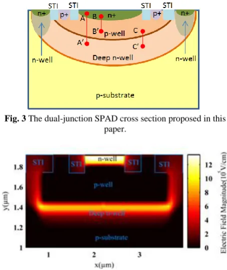
(obtained from the device simulator simulations). Fig. 3 shows the dual-junction SPAD cross-section
proposed in this paper. The proposed SPAD is composed of two separate junctions of n+/well and p-well/deep n-well.
Upon the SPAD biasing above the both junction's breakdown voltages, the electric field in the depletion region of both junctions are engineered to be similarly uniform as shown in Fig. 4. On the other hand, the maximum electric fields in the depletion regions of both junctions are higher than the critical electric field in Silicon. Therefore, when a photon is absorbed beneath
Fig. 1 The p+/n-well SPAD cross-section presented in [15].
Fig. 2 PDP comparison of this work simulation setup and [15].
Fig. 3 The dual-junction SPAD cross section proposed in this paper.
Fig. 4 Dimensional electric field profile of the dual-junction SPAD in 0.17V excess bias.
Iranian Journal of Electrical and Electronic Engineering, Vol. 15, No. 4, December 2019 504 the guard ring, it can also cause impact ionization and
consequently causes avalanche while the carrier diffuses to the active region with the lateral avalanche propagation [21]. Hence, an avalanche pulse in the output terminal is generated according to the absorbed photon.
In conclusion, there is no need to focus photons colliding at the guard ring area of SPAD by the means of an optical μ-lens.
To evaluate the performance of the proposed SPAD, various parameters which are introduced in the previous section are calculated using the simulation setup.
3 Simulation Results
Different physics based models including Shockley Read Hall (SRH) recombination [22, 23], carrier mobility, Auger recombination [24], impact ionization and band to band tunneling [25] are considered in the simulation setup. Tash’s model[26] is used for the mobility modelling , since in the proposed SPAD the electric field strength is relatively high, Klassen’s model [27] is used for SRH modeling since a concentration dependent model is needed. The impact ionization phenomena, is modeled using Selberherr’s model [28].
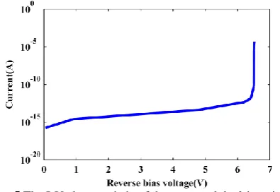
The I-V characteristic of the proposed SPAD is shown in Fig. 5. The breakdown voltage of the proposed SPAD compared with [1] (10.4V implemented in 90 nm CMOS technology) is relatively low since the current SPAD uses n+/p-well active region, though [1] uses n+/p-sub junction active region and the doping impurity in the former case is higher. The proposed SPAD is characterized in Ve = 0.17V (0.17V above the
breakdown voltage). For avalanche probability calculation of SPAD of [15], a similar approach to [20] is maintained.In [29] the history dependent modelfor avalanche probability calculation is used where the history of carriers which cause impact ionization is taken into account. In other words, in history dependent model, the avalanche probability at each point x is not only dependent on the electric field of the corresponding point, but also dependent on the electric field strength of the point at which carrier was created x', as well as dependent on the electric field profile between x and x'. In this model α(x'|x) and β(x'|x) are the history dependent electron and hole ionization coefficients, respectively. pe(x'|x) and ph(x'|x) are electron and hole
ionization probability density at x with electron and hole generated at the x' [29].
( | ) ( | ) exp( ( | ) )
( | ) ( | ) exp( ( | ) )
x e x x h x
p x x x x x x dx dx
p x x x x x x dx dx
(2)In local model the ionization coefficients are expressed as (3) [29]:
( ) exp( / )
( ) exp( / )
h e
h h
E b E
E b E
(3)
Fig. 5 The I-V characteristic of the proposed dual-junction SPAD in reverse bias.
Here be and bh are constants given in [30] and αhand βh
are ionization coefficients of hot carriers [30]. In the history dependent model which is used in this paper, effective electric field is applied instead of E (electric field at point x), which depends on history of carriers. For a constant field E the effective field is [29]:
, , ( ) ( | ) ( ) ( | ) effe e e effe h h x x
E x x E erf
x x
E x x E erf
(4)
Here erf is the error function and:
1 1 log(2) log(2) e e e e h h h h d b erf b E d b erf b E (5)
Here, de and dh are the dead spaces of electron and hole,
which are defined as the minimum distance that a carrier should travel to gain sufficient energy to cause an impact ionization [31]. Dead space for a carrier generated at 0 ≤ x ≤ W can be calculated by [31]:
( ) ( ) ( ) ( ) ie e ih h E d x qE x E d x qE x (6)
Here Ei is the threshold energy for ionization [32] and E
is the electric field .where, q is the unit charge of an electron.
Using (3) the ionization coefficients at position x for a carrier generated at position x', (α(x'|x), β(x'|x)) can be calculated.
According to Fig. 6, if an electron is generated at position x1, it cannot move to x2, due to electric field
repulsion. Hence, the probability of electron generated at x1 causing impact ionization at x2 is negligible. Based
on the similar reason, the probability of a hole generated at x3 causing impact ionization at x2 is negligible, too. In
Iranian Journal of Electrical and Electronic Engineering, Vol. 15, No. 4, December 2019 505 conclusion, the ionization coefficients are modified as
follows:
,
exp( / ( | )),
( | )
0,
h be Eeff e x x x x
x x
x x
(7)
,h
exp( / ( | )),
( | )
0,
h bh Eeff x x x x
x x
x x
(8)
Fig. 7 shows the avalanche probability in the depletion region of both junctions, which is obtained using history dependent model.
The n+/well junction’s depletion region and the p-well/deep n-well junction’s depletion region are shown in Fig. 3. The photons wavelength photons are absorbed close to the surface and the large wavelength photons are absorbed deep inside the bulk.
Equation (1) is used for PDP calculation of the new structure [15]. P is the avalanche probability at position y (Fig. 7). Moreover in order to calculate the fill factor of proposed SPAD, pixel area is calculated using similar peripheral circuit in [33] and considering 90nm technology parameters. Since the active region area in proposed SPAD is 7.06μm2 and the total area of pixel is
16.83μm2, the fill factor of the proposed device is equal
to 42%. Since PDP of the two separate junctions do not overlap in any depth, the PDP of proposed SPAD is the summation of the PDP of two junctions, as shown in Fig. 8.
PDP peak of first junction is 3% at 400nm wavelength and the peak of second junction is 1.5% at 480nm wavelength.
The proposed SPAD should also be characterized in the DCR metric. It should be noted that, the main sources of DCR are direct thermal generation, trap assisted generation and trap assisted tunneling and band to band tunneling generation [34].
The main drawback of the proposed SPAD is the high DCR due to band to band tunneling. Since the doping profiles of 90nm CMOS technology are highly populated to decrease the parasitic resistances, the depletion widths are squeezed which causes higher probability of band to band tunneling. As shown in Fig. 9 the distance of the bands at the first junction is 7nm (BB') and at the second junction is 10nm (CC'). The DCR due to band to band tunneling is calculated according to (9) [33]:
0
( ) ( )
w
BTBT BTBT
DCR S G
y P y dy (9)Here S is the active region area of SPAD and GBTBTis
the band to band tunneling generation rate(which is obtained using the model proposed in [25]), P is the
avalanche probability (shown in Fig. 7) and w is the depletion region width. Since, there are two separate junctions the total DCR is summation of the DCR of each of the two junctions.
In this case, band to band tunneling DCR is calculated as 300kHz at the 0.17V excess bias. It should be noted that high band to band tunneling originated DCR
Fig. 6 A p-n junction depletion cross section and the direction of electric field at the depletion region and three different
locations at the depletion region.
Fig. 7 The probability of avalanche by an electron (Pe) and by a hole (Ph) and by both (P) along the line AA' at the Fig. 3.
Fig. 8 PDP of the dual junction SPAD proposed in this paper and PDP of the SPAD implemented in similar technology [1].
Fig. 9 The band diagram of proposed SPAD along AA' at the Fig. 3.
Table 1 Summary of SPAD main characteristics.
Characteristic Area DCR PDP
0.18μm CMOS [36, 37]
2μm×2μm 200 kHz 11% at 450 nm
130nm CMOS [38] 8μm (active area diameter)
20Hz 20%–25% at 440–570nm 130nm CMOS[39] 10μm (active
area diameter)
100 kHz 34% at 450 nm
90nm CMOS [1] 8μm (diameter) 8.1kHz 16% at 420 nm This work
(90nm CMOS)
2.9μm(active area diameter)
300kHz 16% at 420 nm
Iranian Journal of Electrical and Electronic Engineering, Vol. 15, No. 4, December 2019 506 SPADs can still be utilized in some applications (such
as random number generator). Moreover the DCR can be reduced by correlation evaluation between the two junctions, similar to [35] which is demonstrated to be useful in charged particle positioning applications. In conclusion, the main characteristics of dual-junction SPAD are compared with other similar SPADs in Table 1.
4 Conclusion
Electrical μ-lens is utilized in a STI guard ring based SPAD designed in 90nm standard CMOS technology. The guard ring area itself is used as a photo-sensitive region to collect the impinging carriers generated by the photons. The simulation results show the fill factor can increase to 42% in the proposed SPAD due to carrier collection benth guard ring, utilizing two separate junctions. The PDP of 3% at wavelength between of 400nm is obtained at Ve = 0.17V. Although, the 300kHz DCR of band to band tunneling is present at the Ve = 0.17V.
References
[1] M. A. Karami, “Deep-submicron CMOS single photon detectors and quantum effects,” Ph.D. dissertation, Delft University of Technology, 2011.
[2] C. L. Niclass, A. Rochas, P. A. Besse, and E. Charbon, “A CMOS single photon avalanche diode array for 3D imaging,” in IEEE International Solid-State Circuits Conference (IEEE Cat. No. 04CH37519), pp. 120–517, 2004.
[3] M. Gösch, A. Serov, A. Rochas, H. Blom, T. Anhut, P. A. Besse, R. Popovic, T. Lasser, and R. Rigler, “Parallel single molecule detection with fully integrated single photon 2×2 CMOS detector array,” Journal of Biomedical Optics, Vol. 9, No. 5, pp. 913–922, 2004.
[4] D. Mosconi, D. Stoppa, M. Malfatti, M. Perenzoni, M. Scandiuzzo, and L. Gonzo, “A CMOS sensor based on single photon avalanche diode for fluorescence lifetime measurements,” in IEEE Instrumentation and Measurement Technology Conference Proceedings, pp. 416–419, 2006.
[5] S. Cova, A. Longoni, A. Andreoni, and R. Cubeddu, “A semiconductor detector for measuring ultraweak fluorescence decays with 70 ps FWHM resolution,” IEEE Journal of Quantum Electronics, Vol. 19, No. 4, pp. 630–634, Apr. 1983.
[6] M. Gersbach et al., “Time-correlated fluorescence microscopy using a room temperature solid state single photon sensor,” in International Conference of Near-Field Optics, Nanophotonics, Sep. 2006.
[7] C. L. Niclass, A. Rochas, P. A. Besse, and E. Charbon, “A CMOS single photon avalanche diode array for 3D imaging,” in IEEE International Solid-State Circuits Conference (IEEE Cat. No. 04CH37519), pp. 120–517, 2004.
[8] S. K. Tawfeeq, “A random number generator based on single-photon avalanche photodiode dark counts,” Journal of Lightwave Technology, Vol. 27, No. 24, pp. 5665–5667, 2009.
[9] C. Niclass, A. Rochas, P. A. Besse, R. Popovic, and E. Charbon, “A 4 μs integration time imager based on CMOS single photon avalanche diode technology,” Sensors and Actuators A: Physical, Vol. A130–1, pp. 273–281, Aug. 2006.
[10]F. Zappa, S. Tisa, A. Tosi, and S. Cova, “Principles and features of single-photon avalanche diode arrays,” Sensors and Actuators A: Physical, Vol. 140, No. 1, pp. 103–112, Oct. 2007.
[11]E. A. Webster, and R. K. Henderson. “A TCAD and spectroscopy study of dark count mechanisms in single-photon avalanche diodes,” IEEE Transactions on Electron Devices, Vol. 60, No. 12, pp. 4014– 4019, 2013.
[12]C. Veerappan, Y. Maruyama, and E. Charbon, “Silicon integrated electrical micro-lens for CMOS SPADs based on avalanche propagation phenomenon,” in International Image Sensor Workshop, 2013.
[13]P. Li, J. Pei, L. F. Pan, and H. Zappe, “Fabrication method of low f-number microlens arrays by using surface coating and epoxy dispensing technology,” Journal of Micro/Nanolithography, MEMS, and MOEMS, Vol. 13, No. 2, pp. 023004–023004, 2014.
[14]I. Silvaco, “ATLAS User’s Manual,” Silvaco International Software, Santa Clara, CA, USA, Ver. 5, 2016.
[15]H. Finkelstein, “Shallow-trench-isolation bounded single-photon avalanche diodes in commercial deep submicron CMOS technologies,” Ph.D. dissertation, University of California, San Diego, 2007.
[16]J. P. Donnelly, K. A. McIntosh, D. C. Oakley, A. Napoleone, S. H. Groves, S. Vernon, L. J. Mahoney, K. Molvar, J. Mahan, J. C. Aversa, E. K. Duerr,Z. L. Liau, B. F. Aull, and D. C. Shaver, “1 um Geiger-mode detector development,” in Proceedings of the SPIE, Vol. 5791, pp. 286–292, 2005.
[17]H. Yilmaz, “Optimization and surface-charge sensitivity of high-voltage blocking structures with shallow junctions,” IEEE Transactions on Electron Devices, Vol. 38, No. 7, pp. 1666–1675, 1991.
[18]R. H. Haitz, A. Goetzberger, R. M. Scarlett, and W. Shockley, “Avalanche effects in silicon p-n junctions .I. localized photomultiplication studies on microplasmas,” Journal of Applied Physics, Vol. 34, No. 6, pp. 1581–1589, 1963.
Iranian Journal of Electrical and Electronic Engineering, Vol. 15, No. 4, December 2019 507 [19]N. E. Grant and K. R. McIntosh. “Low surface
recombination velocities achieved by silicon dioxide grown electrochemically in nitric acid,” in 37th IEEE
Photovoltaic Specialists Conference (PVSC), 2011 37th IEEE. IEEE, 2011.
[20]R. J. McIntyre, “On the avalanche initiation probability of avalanche diodes above the breakdown voltage,” IEEE Transactions on Electron Devices, Vol. 20, No. 7, pp. 637–641, 1973.
[21]A. Spinelli and A. L. Lacaita. “Physics and numerical simulation of single photon avalanche diodes,” IEEE Transactions on Electron Devices, Vol. 44, No. 11, pp. 1931–1943, 1997.
[22]W. T. R. W. Shockley and W. T. Read Jr, “Statistics of the recombinations of holes and electrons,” Physical Review, Vol. 87, No. 5, p. 835, 1952.
[23]R. N. Hall, “Electron-hole recombination in germanium,” Physical Review, Vol. 87, No. 2, p. 387, 1952.
[24]J. Dziewior and W. Schmid, “Auger coefficients for highly doped and highly excited silicon,” Applied Physics Letters, Vol. 31, No. 5, pp. 346–348, 1977.
[25]A. Schenk, “Rigorous theory and simplified model of the band-to-band tunneling in silicon,” Solid-State Electronics, Vol. 36, No. 1, pp. 19–34, 1993.
[26]H. Shin, G. M. Yeric, A. F. Tasch, and C. M. Maziar, “Physically-based models for effective mobility and local-field mobility of electrons in MOS inversion layers,” Solid-State Electronics, Vol. 34, No. 6, pp. 545–552, 1991.
[27]D. B. M. Klaassen, “A unified mobility model for device simulation—II. Temperature dependence of carrier mobility and lifetime,” Solid-State Electronics, Vol. 35, No.7, pp. 961–967, 1992.
[28]S. Selberherr, Analysis and simulation of semiconductor devices. Springer Science & Business Media, 2012.
[29]R. J. McIntyre, “A new look at impact ionization-Part I: A theory of gain, noise, breakdown probability, and frequency response,” IEEE Transactions on Electron Devices, Vol. 46, No. 8, pp. 1623–1631, 1999.
[30]R. Van Overstraeten and H. De Man, “Measurement of the ionization rates in diffused silicon pn junctions,” Solid-State Electronics, Vol. 13, No. 5, pp. 583–608, 1970.
[31]M. M. Hayat, W. L. Sargeant, and B. E. Saleh, “Effect of dead space on gain and noise in Si and GaAs avalanche photodiodes,” IEEE Journal of Quantum Electronics, Vol. 28, No. 5, pp. 1360– 1365, 1992.
[32]A. Spinelli, A. Pacelli, and A. L. Lacaita, “Dead space approximation for impact ionization in silicon,” Applied Physics Letters, Vol. 69, No. 24, pp. 3707–3709, 1996.
[33]I. Vornicu, R. Carmona‐Galán, B. Pérez‐Verdú, and Á. Rodríguez‐Vázquez, “Compact CMOS active quenching/recharge circuit for SPAD arrays,” International Journal of Circuit Theory and Applications, Vol. 44, No. 4, pp. 917–928, 2015.
[34]Y. Xu, P. Xiang, and X. Xie, “Comprehensive understanding of dark count mechanisms of single-photon avalanche diodes fabricated in deep sub-micron CMOS technologies,” Solid-State Electronics, Vol. 129, pp. 168–174, 2016.
[35]L. Pancheri, A. Ficorella, P. Brogi, G. Collazuol, G. F. Dalla Betta, P. S. Marrocchesi, F. Morsani, L. Ratti, A. Savoy-Navarro, and A. Sulaj, “First demonstration of a two-tier pixelated avalanche sensor for charged particle detection,” IEEE Journal of the Electron Devices Society, Vol. 5, No. 5, pp.404–410, 2017.
[36]H. Finkelstein, M. J. Hsu, S. Zlatanovic, and S. Esener, “Performance trade-offs in single-photon avalanche diode miniaturization,” Review of Scientific Instruments, Vol. 78, No. 10, p. 103103, 2007.
[37]M. J. Hsu, H. Finkelstein, and S. C. Esener, “A CMOS STI-bound single-photon avalanche diode with 27-ps timing resolution and a reduced diffusion tail,” IEEE Electron Device Letters; Vol. 30, No. 6, pp. 641-963, Jun. 2009.
[38]J. A. Richardson, L. A. Grant, and R. K. Henderson, “Low dark count single-photon avalanche diode structure compatible with standard nanometer scale CMOS technology,” IEEE Photonics Technology Letters, Vol. 21, No. 14, pp. 1020–1022, 2009.
[39]M. Gersbach, Y. Maruyama, E. Labonne, J. Richardson, R. Walker, L. Grant, R. Henderson, F. Borghetti, D. Stoppa, and E. Charbon, “A parallel 32×32 time-to-digital converter array fabricated in a 130 nm imaging CMOS technology,” in IEEE Proceedings of ESSCIRC, pp. 196–199, Sep. 2009.
S. Ejdehakosh born in Shiraz, Iran. She received her bachelor’s degree in Electrical Engineering from Shiraz University of Technology. She was a master student in Electrical Engineering (Electronics) in School of Electrical Engineering in Iran University of Science and Technology (IUST), in which she graduated in 2018.
Iranian Journal of Electrical and Electronic Engineering, Vol. 15, No. 4, December 2019 508
M. A. Karami born in Tehran, Iran in 1983. He got B.Sc. from Shahid Beheshti University in 2005, M.Sc. from University of Tehran in 2007, and Ph.D. degree from Tu Delft in 2011, all in Electronic Engineering. He is currently an Associate Professor in School of Electrical Engineering in Iran University of Science and Technology. His area of expertise is in semiconductor devices and image sensors.
© 2019 by the authors. Licensee IUST, Tehran, Iran. This article is an open access article distributed under the terms and conditions of the Creative Commons Attribution-NonCommercial 4.0 International (CC BY-NC 4.0) license (https://creativecommons.org/licenses/by-nc/4.0/).