Adv. Radio Sci., 8, 161–166, 2010 www.adv-radio-sci.net/8/161/2010/ doi:10.5194/ars-8-161-2010
© Author(s) 2010. CC Attribution 3.0 License.
Advances in
Radio Science
Non-linear behaviour of charge-pump phase-locked loops
C. Wiegand1,2, C. Hedayat1, and U. Hilleringmann1,2
1Fraunhofer ENAS, Department Advanced System Engineering (ASE), Warburger Str. 100, 33098 Paderborn, Germany 2University of Paderborn, Department of Sensor Technology Warburger Str. 100, 33098 Paderborn, Germany
Abstract. The analysis of the mixed analogue and digital structure of charge-pump phase-locked loops (CP-PLL) is a challenge in modelling and simulation. In most cases the system is designed and characterized using its continuous linear model or its discrete linear model neglecting its non-linear switching behaviour. I.e., the time-varying model is approximated by a time-invariant representation using its av-erage dynamics. Depending on what kind of phase detector is used, the scopes of validity of these approximations are different. Here, a preeminent characterization and simula-tion technique based on the systems event-driven feature is presented, merging the logical and analogue inherent char-acteristics of the system. In particular, the high-grade non-linear locking process and the dead-zone are analyzed.
1 Introduction
Phase-locked loops (PLL) are widely used and can be uti-lized to synchronize an oscillator in phase and frequency. If the PLL is absolutely synchronized, the phase error between the input signal and the oscillator signal is minimal. As soon as a phase error occurs, the oscillator will be readjusted un-til the phase error is again minimal (Gardner, 1980, 1966; Best, 1993; Shu and Sanchez-Sinencio, 2005). Depending on what kind of phase detector (PD) is used, the lock mar-gin sensitively varies (Best, 1993; Wolaver, 1991). If the PLL is stable and the loop bandwidth is wide enough, the locked system has a dynamic, which can be described by an averaged/linearized model. By using a tri state phase and frequency detector (PFD), the PLL is locked if the absolute phase error remains smaller than 2π (Best, 1993; Wolaver, 1991; Den Dulk, 1988). Generally, there are two operating
Correspondence to: C. Wiegand ([email protected])
ranges in CP-PLL systems: the linear operating range and the non-linear operating range. The linear operating range is de-fined by the linear model of the PLL and can be assigned as that range where the PLL is locked. Even if the PLL is locked and all non-idealities (dead-zone, non-linear characteristic of the VCO etc.) are neglected, the PLL possesses a weak non-linear behaviour caused by the logical switching of the PFD. Furthermore, while the PLL is out-of-lock, the system shows a high-grade non-linear behaviour. The non-linear operat-ing range is also called the pull-in range. For this purpose, the PLL is characterized by considering the switching of the PFD. In addition a new lock detection circuitry delivering re-liable information about the status of the output clock signal is presented. This is a direct consequence of the character-ization of the switching behaviour. The proposed method monitors and detects when the phase error between the ref-erence and the synthesized output clock leaves (out-of lock) or enters (locked) the phase and frequency detector’s linear range (ϕe∈ [−2π,2π]). For this, the digital information of the PFD monitoring the closed loop is scanned along the tran-sient progress of the system. We will focus here on the case of a tri state PFD. A methodology is presented, which allows to identify and to characterize a CP-PLL by means of its in-herent non-linear switching behaviour.
Beside the switching of the PLL, another non-linearity is considered and characterized. The dead-zone due to the PFD and the charge-pump, mostly considered as a static non-linearity embedded into the linear continuous approximation, represents a dynamic non-ideality caused by the delays of the PFD’s logic and the charge-pump’s slew-rate (Hedayat et al., 1999). An advanced PFD model for accurate simulations of CP-PLL systems is presented.
162 C. Wiegand et al.: Non-linear behaviour of charge-pump phase-locked loops
havioural non-linear model of the dead-zone is introduced.
In section 2 a direct implication (application) of section 1.3
is presented.
1
Modelling
The PLL offers various models and various non-linearities.
In the following, the main focus is pointed upon the
non-linear behaviour of the PFD. For this, the switching
prop-erties and the linear model are compared. Additionally, an
advanced PFD model is introduced.
1.1
Architecture
For simplicity, an integer-N PLL frequency synthesizer
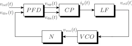
ar-chitecture is considered (see fig. 1). The PLL consists of five
functional blocks.
𝑣ref(𝑡)
𝑣div(𝑡)
𝑣up(𝑡)
𝑣dn(𝑡)
𝑖p(𝑡) 𝑣ctl(𝑡)
𝑣vco(𝑡)
𝑃 𝐹 𝐷 𝐶𝑃 𝐿𝐹
𝑉 𝐶𝑂 𝑁
Fig. 1. Schematic representation of a charge-pump phase-locked loop.
– PFD: The phase and frequency detector is a purely
digi-tal device having two output signals (
𝑣
up(𝑡)
and
𝑣
dn(𝑡)
)
and is driven by the falling (or rising) edges of its input
signals (reference signal
𝑣
ref(𝑡)
and VCO signal
𝑣
vco(𝑡)
[if no divider is used] respectively the divider output
sig-nal
𝑣
div(𝑡)
) estimating the phase error between
𝑣
ref(𝑡)
and
𝑣
vco,div(𝑡)
.
– CP: The charge-pump delivers a current
𝑖
p(𝑡)
, driven
by the PFD outputs
𝑣
up(𝑡)
and
𝑣
dn(𝑡)
.
– LF: The loop filter is a low-pass filter, which converts
the current
𝑖
pinto a voltage
𝑣
ctl(𝑡)
filtering the
alternat-ing current component.
– VCO: The oscillating output
𝑣
vco(𝑡)
of the VCO is
con-trolled by the loop filter’s output voltage
𝑣
ctl(𝑡)
.
– N: The divider is a periodic or a modulo N counter,
al-lowing frequency multiplication (
𝑓
vco⋅
𝑁
=
𝑓
div).
1.2
Linearized Continuous Model
It is assumed, that the system is stable. This is mainly
as-sured when the denominator of the following phase transfer
function (second order PLL) is hurwitzian and the reference
frequency
𝑓
refis notably higher than the loop natural
fre-quency
𝑓
n=
𝜔
n/(2𝜋)
(Gardner, 1980). In general, it can be
said, that if a second order CP-PLL is locked (the absolute
phase error
∣
𝜑
e∣remains smaller than
2𝜋
), the linear
con-tinuous approximation can be used to describe the average
dynamic behaviour. It holds
𝐻(𝑠) =
2𝜁𝜔
n𝑠
+
𝜔
2 n
𝑠
2+ 2𝜁𝜔
n
𝑠
+
𝜔
n2,
(1)
where
𝜁
=
𝑅
1𝐶
12
𝜔
n(2)
denotes the damping factor and
𝜔
n=
√
𝐾/𝐶
1represents the
natural frequency, where
𝐾
=
𝐾
v𝐼
pis called the loop gain.
Obviously, the linear model can not describe the non-linear
pull-in process.
1.3
Non-linear Model and Characterization
𝑣ref ↓
𝑣ref ↓
𝑣ref ↓
𝑣vco,div↓ 𝑣vco,div↓
𝑣vco,div↓ −1 0 +1
Fig. 2. Finite state machine of the phase and frequency detector driven by the falling edges of the reference signal 𝑣ref(𝑡) and the VCO or the divider output signal𝑣vco(𝑡)respectively𝑣div(𝑡).
In the following, the non-linear signature of the switched
differential equation system caused by the finite state
ma-chine is characterized. For this, the VCO is considered as
an ideal integrator. Non-idealities like dead-zone and
non-linear characteristic of the VCO are neglected. With this
assumption, the only non-linearity of the loop is related to
the switching behaviour of the digital PFD. The traditional
PFD (tri state PFD) is a sequential circuit, driven by the
falling or rising edges of its input signals (reference signal
𝑣
refand VCO respectively divider signal
𝑣
vco,div, where the
subscripts ”vco” or ”div” denote a PLL without divider
re-spectively with divider). In a more abstract view, the PFD
can be represented by a finite state machine consisting of
three states. Fig. 2 shows the state graph of the PFD, driven
by a given type of edges (falling edges or rising edges of
𝑣
refand
𝑣
vco,div). The states of the PFD are represented by the
logical output signals
𝑣
upand
𝑣
dnand can be defined with
{
𝑣
up= 0;
𝑣
dn= 1
}
=
ˆ
𝒮
−1,
{
𝑣
up= 0;
𝑣
dn= 0
}
=
ˆ
𝒮0
and
{
𝑣
up= 1;
𝑣
dn= 0
}
=
ˆ
𝒮+1
. It is obvious, that the
charge-pump is controlled by these states, i. e. by the PFD output
signals
𝑣
upand
𝑣
dn. The interrelation between the states of
the PFD and the solution of the differential equation of the
switching system is presented in equations (3) and (5).
𝒙
n+1=
Φ
(𝑡
n−
𝑡
n+1)
𝒙
n+
∫
𝑡n+1𝑡n
Φ
(𝑡
n−
𝜏
)
𝒃
𝑖
p(
𝒮
(𝜏
)) d𝜏
(3)
Fig. 1. Schematic representation of a charge-pump phase-locked
loop.
PFD state sequences are considered. The last subsection of Sect. 2 is dedicated to a particular non-linearity. A be-havioural non-linear model of the dead-zone is introduced. In Sect. 3 a direct implication (application) of Sect. 2.3 is presented.
2 Modelling
The PLL offers various models and various non-linearities. In the following, the main focus is pointed upon the non-linear behaviour of the PFD. For this, the switching prop-erties and the linear model are compared. Additionally, an advanced PFD model is introduced.
2.1 Architecture
For simplicity, an integer-N PLL frequency synthesizer ar-chitecture is considered (see Fig. 1). The PLL consists of five functional blocks.
– PFD: The phase and frequency detector is a purely dig-ital device having two output signals (vup(t )andvdn(t )) and is driven by the falling (or rising) edges of its input signals (reference signalvref(t )and VCO signalvvco(t ) [if no divider is used] respectively the divider output sig-nalvdiv(t )) estimating the phase error between vref(t ) andvvco,div(t ).
– CP: The charge-pump delivers a currentip(t ), driven by the PFD outputsvup(t )andvdn(t ).
– LF: The loop filter is a low-pass filter, which converts the currentipinto a voltagevctl(t )filtering the alternat-ing current component.
– VCO: The oscillating outputvvco(t )of the VCO is con-trolled by the loop filter’s output voltagevctl(t ). – N: The divider is a periodic or a modulo N counter,
al-lowing frequency multiplicationfvco=fdiv·N. 2.2 Linearized continuous model
It is assumed, that the system is stable. This is mainly assured when the denominator of the following phase transfer
func-havioural non-linear model of the dead-zone is introduced.
In section 2 a direct implication (application) of section 1.3
is presented.
1
Modelling
The PLL offers various models and various non-linearities.
In the following, the main focus is pointed upon the
non-linear behaviour of the PFD. For this, the switching
prop-erties and the linear model are compared. Additionally, an
advanced PFD model is introduced.
1.1
Architecture
For simplicity, an integer-N PLL frequency synthesizer
ar-chitecture is considered (see fig. 1). The PLL consists of five
functional blocks.
𝑣ref(𝑡)
𝑣div(𝑡)
𝑣up(𝑡)
𝑣dn(𝑡)
𝑖p(𝑡) 𝑣ctl(𝑡)
𝑣vco(𝑡)
𝑃 𝐹 𝐷 𝐶𝑃 𝐿𝐹
𝑉 𝐶𝑂 𝑁
Fig. 1. Schematic representation of a charge-pump phase-locked loop.
– PFD: The phase and frequency detector is a purely
digi-tal device having two output signals (
𝑣
up(
𝑡
)
and
𝑣
dn(
𝑡
)
)
and is driven by the falling (or rising) edges of its input
signals (reference signal
𝑣
ref(
𝑡
)
and VCO signal
𝑣
vco(
𝑡
)
[if no divider is used] respectively the divider output
sig-nal
𝑣
div(
𝑡
)
) estimating the phase error between
𝑣
ref(
𝑡
)
and
𝑣
vco,div(
𝑡
)
.
– CP: The charge-pump delivers a current
𝑖
p(
𝑡
)
, driven
by the PFD outputs
𝑣
up(
𝑡
)
and
𝑣
dn(
𝑡
)
.
– LF: The loop filter is a low-pass filter, which converts
the current
𝑖
pinto a voltage
𝑣
ctl(
𝑡
)
filtering the
alternat-ing current component.
– VCO: The oscillating output
𝑣
vco(
𝑡
)
of the VCO is
con-trolled by the loop filter’s output voltage
𝑣
ctl(
𝑡
)
.
– N: The divider is a periodic or a modulo N counter,
al-lowing frequency multiplication (
𝑓
vco⋅
𝑁
=
𝑓
div).
1.2
Linearized Continuous Model
It is assumed, that the system is stable. This is mainly
as-sured when the denominator of the following phase transfer
function (second order PLL) is hurwitzian and the reference
frequency
𝑓
refis notably higher than the loop natural
fre-quency
𝑓
n=
𝜔
n/
(2
𝜋
)
(Gardner, 1980). In general, it can be
said, that if a second order CP-PLL is locked (the absolute
phase error
∣
𝜑
e∣
remains smaller than
2
𝜋
), the linear
con-tinuous approximation can be used to describe the average
dynamic behaviour. It holds
𝐻
(
𝑠
) =
2
𝜁𝜔
n𝑠
+
𝜔
2 n
𝑠
2+ 2
𝜁𝜔
n
𝑠
+
𝜔
n2,
(1)
where
𝜁
=
𝑅
1𝐶
12
𝜔
n(2)
denotes the damping factor and
𝜔
n=
√
𝐾/𝐶
1represents the
natural frequency, where
𝐾
=
𝐾
v𝐼
pis called the loop gain.
Obviously, the linear model can not describe the non-linear
pull-in process.
1.3
Non-linear Model and Characterization
𝑣ref ↓
𝑣ref ↓
𝑣ref ↓
𝑣vco,div↓ 𝑣vco,div↓
𝑣vco,div ↓ −1 0 +1
Fig. 2. Finite state machine of the phase and frequency detector driven by the falling edges of the reference signal𝑣ref(𝑡)and the VCO or the divider output signal𝑣vco(𝑡)respectively𝑣div(𝑡).
In the following, the non-linear signature of the switched
differential equation system caused by the finite state
ma-chine is characterized. For this, the VCO is considered as
an ideal integrator. Non-idealities like dead-zone and
non-linear characteristic of the VCO are neglected. With this
assumption, the only non-linearity of the loop is related to
the switching behaviour of the digital PFD. The traditional
PFD (tri state PFD) is a sequential circuit, driven by the
falling or rising edges of its input signals (reference signal
𝑣
refand VCO respectively divider signal
𝑣
vco,div, where the
subscripts ”vco” or ”div” denote a PLL without divider
re-spectively with divider). In a more abstract view, the PFD
can be represented by a finite state machine consisting of
three states. Fig. 2 shows the state graph of the PFD, driven
by a given type of edges (falling edges or rising edges of
𝑣
refand
𝑣
vco,div). The states of the PFD are represented by the
logical output signals
𝑣
upand
𝑣
dnand can be defined with
{
𝑣
up= 0;
𝑣
dn= 1
}
=
ˆ
𝒮
−1,
{
𝑣
up= 0;
𝑣
dn= 0
}
=
ˆ
𝒮
0and
{
𝑣
up= 1;
𝑣
dn= 0
}
=
ˆ
𝒮
+1. It is obvious, that the
charge-pump is controlled by these states, i. e. by the PFD output
signals
𝑣
upand
𝑣
dn. The interrelation between the states of
the PFD and the solution of the differential equation of the
switching system is presented in equations (3) and (5).
𝒙
n+1=
Φ
(
𝑡
n−
𝑡
n+1)
𝒙
n+
∫
𝑡n+1𝑡n
Φ
(
𝑡
n−
𝜏
)
𝒃
𝑖
p(
𝒮
(
𝜏
)) d
𝜏
(3)
Fig. 2. Finite state machine of the phase and frequency detector
driven by the falling edges of the reference signalvref(t )and the VCO or the divider output signalvvco(t )respectivelyvdiv(t ). tion (second order PLL) is hurwitzian and the reference fre-quencyfrefis notably higher than the loop natural frequency fn=ωn/(2π )(Gardner, 1980). In general, it can be said, that if a second order CP-PLL is locked (the absolute phase error |ϕe| remains smaller than 2π), the linear continuous approximation can be used to describe the average dynamic behaviour. It holds
H (s)= 2ζ ωns+ω 2 n s2+2ζ ω
ns+ωn2
, (1)
where
ζ=R1C1
2 ωn (2)
denotes the damping factor andωn= √
K/C1represents the natural frequency, whereK=KvIp is called the loop gain. Obviously, the linear model can not describe the non-linear pull-in process.
2.3 Non-linear model and characterization
In the following, the non-linear signature of the switched dif-ferential equation system caused by the finite state machine is characterized. For this, the VCO is considered as an ideal integrator. Non-idealities like dead-zone and non-linear char-acteristic of the VCO are neglected. With this assumption, the only non-linearity of the loop is related to the switching behaviour of the digital PFD. The traditional PFD (tri state PFD) is a sequential circuit, driven by the falling or rising edges of its input signals (reference signalvrefand VCO re-spectively divider signalvvco,div, where the subscripts “vco” or “div” denote a PLL without divider respectively with di-vider). In a more abstract view, the PFD can be represented by a finite state machine consisting of three states. Figure 2 shows the state graph of the PFD, driven by a given type of edges (falling edges or rising edges ofvrefandvvco,div). The states of the PFD are represented by the logical output signals
vupandvdnand can be defined with{vup=0;vdn=1} ˆ=S−1, {vup=0;vdn=0} ˆ=S0and{vup=1;vdn=0} ˆ=S+1. It is ob-vious, that the charge-pump is controlled by these states, i. e. by the PFD output signalsvupandvdn. The interrelation be-tween the states of the PFD and the solution of the differential equation of the switching system is presented in Eqs. (3) and (5).
xn+1=8(tn−tn+1)xn+
C. Wiegand et al.: Non-linear behaviour of charge-pump phase-locked loops 163
C. Wiegand et al.: Non-linear behaviour of Charge-Pump Phase-Locked Loops
3
Φ
(
⋅
)
represents the state-transition matrix,
𝒃
is the control
matrix, the vector
𝒙
is denoted as the vector of state
vari-ables and
𝑖
p(
𝒮
(𝜏
))
is the charge-pump current controlled by
the states
𝒮
(
⋅
)
of the PFD, where
𝒮
(
⋅
)
∈
[
𝒮+1
,
𝒮0
,
𝒮
−1]
and
is controlled by the reference signal
𝑣
ref(𝑡)
and the output
signal
𝑣
vco,div. Therefore,
𝒮
(𝜏)
is a function of
𝑣
ref(𝜏
)
and
𝑣
vco,div(𝜏)
:
𝒮
(𝜏
) =
𝒮
(𝑣
ref(𝜏
), 𝑣
vco,div(𝜏
))
(4)
Obviously, there are three states modulating the charge-pump
current into three constant values.
It holds
𝑖
p(
𝒮
(𝜏
))
∈
[+𝐼
p,
0,
−
𝐼
p]
. Thus, equation (5) results:
𝒙
n+1=
Φ
(𝑡
n−
𝑡
n+1)
𝒙
n+
⎧
⎨
⎩
+𝐼
p∫
𝑡n+1𝑡n
Φ
(𝑡
n−
𝜏
)
𝒃
d𝜏 ,
𝒮+1
0
,
𝒮0
−
𝐼
p∫
𝑡n+1𝑡n
Φ
(𝑡
n−
𝜏
)
𝒃
d𝜏 ,
𝒮
−1(5)
By using a first order passive
𝑅
−
𝐶
loop filter (Gardner,
1980; Hedayat et al., 1997; Daniels and Farrell, 2008), a
sec-ond order loop results.
Time𝑡[𝜇s]
Fr eq u en cy 𝑓 [H z] Nonlinear Linear
0 0.5 1 1.5 2
𝑓0
Fig. 3. While the second order PLL delivers a phase error between
−2𝜋 < 𝜑e < 2𝜋the PLL is called locked and the linear
approxi-mation provides a good average conformity.
As it can be observed on fig. 3, when the loop is locked (i. e.
the absolute phase error
∣
𝜑
e∣remains smaller than
2𝜋
) and
stable with a reference frequency
𝑓
refnotably higher than the
loop natural frequency, the linearized continuous-time model
represents a good approximation of the average behaviour. In
addition to the damped sinusoidal dynamics, the non-linear
model possesses a comp-shaped behaviour (illustrated in fig.
3). This comb-shaped structure indicates the state
𝒮
(𝑡)
of
the PFD. The heights of the peaks is correlated to the
prod-uct of the loop filters resistor
𝑅
1and the charge-pump
cur-rent
𝑖
p(
𝒮
(𝜏
))
. All the peaks of the comb-shaped structure
directed upwards are associated to the logical state
𝒮+1
. The
peaks directed downwards are related to the PFD state
𝒮
−1.
When the linear model matches with the non-linear one, the
PFD is at the state
𝒮0
. Considering fig. 3 two state sequences
can be identified. The PFD sequence corresponding to a
dig-ital overshoot is defined as
𝒮
↑=
{𝒮+1
,
𝒮0
,
𝒮
−1},
(6)
where the subscripted down arrow emphasizes the direction
and the state sequence of a digital undershoot is defined as
𝒮
↓=
{𝒮
−1,
𝒮0
,
𝒮+1}
.
(7)
Generally an overshoot or an undershoot occurs if the
damp-ing
𝜁
is less than
1.2
. In the case of a third order or a high
order PLL system (the second order filter consists of the first
order passive loop filter with a parallel smoothing
capaci-tor [see (Shu and Sanchez-Sinencio, 2005; Hedayat et al.,
1999)]), the state sequences
𝒮
↓and
𝒮
↑do not identify the
real frequency
𝑓
vco(voltage
𝑣
ctl) overshoot or undershoot.
Only zero crossings of the phase error
𝜑
eare detected by
these state sequences, because the phase and frequency
de-tector operates on the phase of the reference (
𝑣
ref) and
di-vider (resp. VCO) output signal (
𝑣
vco,div). For this reason,
the logical signature can be used for characterizing the
dy-namic behaviour of the PLL. While the PLL is out-of-lock
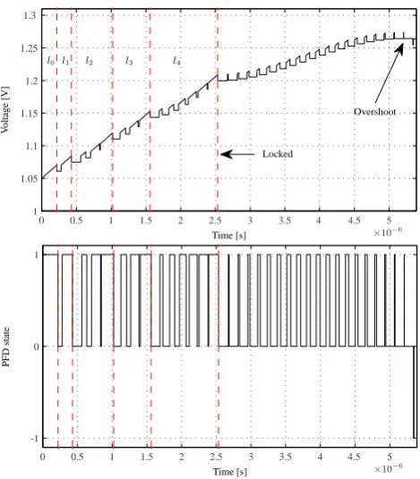
𝑙0 𝑙1 𝑙2 𝑙3 𝑙4
Time [s] V o lta g e [V ] Time [s] PFD sta te Overshoot Locked
0 0.5 1 1.5 2 2.5 3 3.5 4 4.5 5
×10−6
0 0.5 1 1.5 2 2.5 3 3.5 4 4.5 5
×10−6
-1 0 1 1 1.05 1.1 1.15 1.2 1.25 1.3
Fig. 4. The pull-in process is divided into five ranges 𝑟𝑖 (𝑖 ∈
[0,1,2,3,4]) and the course of events of the PFD’s states𝒮.
(phase error
∣
𝜑
e∣>
2𝜋
), the linear model is no more valid.
Therefore the pull-in process has to be analyzed by means
of the non-linear pulse width modulated (PWM) model (see
Fig. 3. While the second order PLL delivers a phase error between
−2π < ϕe<2πthe PLL is called locked and the linear
approxima-tion provides a good average conformity.
Z tn+1 tn
8(tn−τ )bip(S(τ ))dτ (3) 8(·) represents the matrix exponential of the state matrix, b is the control vector, the vector x is denoted as the vector of state variables and ip(S(τ )) is the charge-pump current controlled by the states S(·) of the PFD, where
S(·)∈ {S+1,S0,S−1}and is controlled by the reference sig-nalvref(t )and the output signalvvco,div. Therefore,S(τ )is a function ofvref(τ )andvvco,div(τ ):
S(τ )=S(vref(τ ), vvco,div(τ )) (4) Obviously, there are three states modulating the charge-pump current into three constant values. It holdsip(S(τ ))∈ +
Ip,0,−Ip . Thus, Eq. (5) results:
xn+1=8(tn−tn+1)xn+
+Ip Z tn+1
tn
8(tn−τ )bdτ ,S+1
0 ,S0
−Ip Z tn+1
tn
8(tn−τ )bdτ ,S−1 (5)
By using a first order passive R−C loop filter (Gardner, 1980; Hedayat et al., 1997; Daniels and Farrell, 2008), a sec-ond order loop results.
As it can be observed on Fig. 3, when the loop is locked (i.e. the absolute phase error|ϕe|remains smaller than 2π) and stable with a reference frequency fref notably higher than the loop natural frequency, the linearized continuous-time model represents a good approximation of the average behaviour. In addition to the damped sinusoidal dynamics, the non-linear model possesses a comp-shaped behaviour (il-lustrated in Fig. 3). This comb-shaped structure indicates the stateS(t )of the PFD. The heights of the peaks is cor-related to the product of the loop filters resistorR1and the charge-pump currentip(S(τ )). All the peaks of the comb-shaped structure directed upwards are associated to the log-ical stateS+1. The peaks directed downwards are related to
C. Wiegand et al.: Non-linear behaviour of Charge-Pump Phase-Locked Loops 3
Φ(⋅) represents the state-transition matrix, 𝒃 is the control
matrix, the vector 𝒙 is denoted as the vector of state
vari-ables and𝑖p(𝒮(𝜏))is the charge-pump current controlled by
the states𝒮(⋅)of the PFD, where𝒮(⋅)∈[𝒮+1,𝒮0,𝒮−1]and
is controlled by the reference signal 𝑣ref(𝑡) and the output
signal𝑣vco,div. Therefore,𝒮(𝜏)is a function of𝑣ref(𝜏)and 𝑣vco,div(𝜏):
𝒮(𝜏) =𝒮(𝑣ref(𝜏), 𝑣vco,div(𝜏)) (4)
Obviously, there are three states modulating the charge-pump current into three constant values. It holds 𝑖p(𝒮(𝜏)) ∈
[+𝐼p,0,−𝐼p]. Thus, equation (5) results:
𝒙n+1=Φ(𝑡n−𝑡n+1)𝒙n+
⎧ ⎨ ⎩
+𝐼p
∫ 𝑡n+1
𝑡n
Φ(𝑡n−𝜏)𝒃d𝜏 ,𝒮+1
0 ,𝒮0
−𝐼p
∫ 𝑡n+1
𝑡n
Φ(𝑡n−𝜏)𝒃d𝜏 ,𝒮−1
(5)
By using a first order passive 𝑅−𝐶 loop filter (Gardner, 1980; Hedayat et al., 1997; Daniels and Farrell, 2008), a sec-ond order loop results.
Time𝑡[𝜇s]
Fr eq u en cy 𝑓 [H z] Nonlinear Linear
0 0.5 1 1.5 2
𝑓0
Fig. 3. While the second order PLL delivers a phase error between
−2𝜋 < 𝜑e <2𝜋the PLL is called locked and the linear
approxi-mation provides a good average conformity.
As it can be observed on fig. 3, when the loop is locked (i. e. the absolute phase error∣𝜑e∣ remains smaller than 2𝜋) and
stable with a reference frequency𝑓ref notably higher than the
loop natural frequency, the linearized continuous-time model represents a good approximation of the average behaviour. In addition to the damped sinusoidal dynamics, the non-linear model possesses a comp-shaped behaviour (illustrated in fig. 3). This comb-shaped structure indicates the state 𝒮(𝑡)of the PFD. The heights of the peaks is correlated to the prod-uct of the loop filters resistor𝑅1 and the charge-pump
cur-rent𝑖p(𝒮(𝜏)). All the peaks of the comb-shaped structure
directed upwards are associated to the logical state𝒮+1. The
peaks directed downwards are related to the PFD state𝒮−1.
When the linear model matches with the non-linear one, the PFD is at the state𝒮0. Considering fig. 3 two state sequences
can be identified. The PFD sequence corresponding to a dig-ital overshoot is defined as
𝒮↑ ={𝒮+1, 𝒮0,𝒮−1}, (6)
where the subscripted down arrow emphasizes the direction and the state sequence of a digital undershoot is defined as
𝒮↓ ={𝒮−1,𝒮0, 𝒮+1}. (7)
Generally an overshoot or an undershoot occurs if the damp-ing𝜁 is less than1.2. In the case of a third order or a high order PLL system (the second order filter consists of the first order passive loop filter with a parallel smoothing capaci-tor [see (Shu and Sanchez-Sinencio, 2005; Hedayat et al., 1999)]), the state sequences 𝒮↓ and 𝒮↑ do not identify the
real frequency 𝑓vco (voltage 𝑣ctl) overshoot or undershoot.
Only zero crossings of the phase error 𝜑e are detected by
these state sequences, because the phase and frequency de-tector operates on the phase of the reference (𝑣ref) and
di-vider (resp. VCO) output signal (𝑣vco,div). For this reason,
the logical signature can be used for characterizing the dy-namic behaviour of the PLL. While the PLL is out-of-lock
𝑙0 𝑙1 𝑙2 𝑙3 𝑙4
Time [s] V o lta g e [V ] Time [s] PFD sta te Overshoot Locked
0 0.5 1 1.5 2 2.5 3 3.5 4 4.5 5
×10−6
0 0.5 1 1.5 2 2.5 3 3.5 4 4.5 5
×10−6
-1 0 1 1 1.05 1.1 1.15 1.2 1.25 1.3
Fig. 4. The pull-in process is divided into five ranges 𝑟𝑖 (𝑖 ∈
[0,1,2,3,4]) and the course of events of the PFD’s states𝒮.
(phase error∣𝜑e∣ > 2𝜋), the linear model is no more valid.
Therefore the pull-in process has to be analyzed by means of the non-linear pulse width modulated (PWM) model (see
C. Wiegand et al.: Non-linear behaviour of Charge-Pump Phase-Locked Loops 3
Φ(⋅) represents the state-transition matrix, 𝒃 is the control
matrix, the vector 𝒙 is denoted as the vector of state
vari-ables and𝑖p(𝒮(𝜏))is the charge-pump current controlled by
the states𝒮(⋅)of the PFD, where𝒮(⋅)∈ [𝒮+1,𝒮0,𝒮−1]and
is controlled by the reference signal 𝑣ref(𝑡) and the output
signal𝑣vco,div. Therefore,𝒮(𝜏)is a function of𝑣ref(𝜏)and 𝑣vco,div(𝜏):
𝒮(𝜏) =𝒮(𝑣ref(𝜏), 𝑣vco,div(𝜏)) (4)
Obviously, there are three states modulating the charge-pump current into three constant values. It holds 𝑖p(𝒮(𝜏)) ∈
[+𝐼p,0,−𝐼p]. Thus, equation (5) results:
𝒙n+1=Φ(𝑡n−𝑡n+1)𝒙n+
⎧ ⎨ ⎩
+𝐼p
∫ 𝑡n+1
𝑡n
Φ(𝑡n−𝜏)𝒃d𝜏 ,𝒮+1
0 ,𝒮0
−𝐼p
∫ 𝑡n+1
𝑡n
Φ(𝑡n−𝜏)𝒃d𝜏 ,𝒮−1
(5)
By using a first order passive𝑅− 𝐶 loop filter (Gardner, 1980; Hedayat et al., 1997; Daniels and Farrell, 2008), a sec-ond order loop results.
Time𝑡[𝜇s]
Fr eq u en cy 𝑓 [H z] Nonlinear Linear
0 0.5 1 1.5 2
𝑓0
Fig. 3. While the second order PLL delivers a phase error between
−2𝜋 < 𝜑e < 2𝜋the PLL is called locked and the linear
approxi-mation provides a good average conformity.
As it can be observed on fig. 3, when the loop is locked (i. e. the absolute phase error ∣𝜑e∣remains smaller than 2𝜋) and
stable with a reference frequency𝑓ref notably higher than the
loop natural frequency, the linearized continuous-time model represents a good approximation of the average behaviour. In addition to the damped sinusoidal dynamics, the non-linear model possesses a comp-shaped behaviour (illustrated in fig. 3). This comb-shaped structure indicates the state𝒮(𝑡) of the PFD. The heights of the peaks is correlated to the prod-uct of the loop filters resistor𝑅1 and the charge-pump
cur-rent 𝑖p(𝒮(𝜏)). All the peaks of the comb-shaped structure
directed upwards are associated to the logical state𝒮+1. The
peaks directed downwards are related to the PFD state𝒮−1.
When the linear model matches with the non-linear one, the PFD is at the state𝒮0. Considering fig. 3 two state sequences
can be identified. The PFD sequence corresponding to a dig-ital overshoot is defined as
𝒮↑={𝒮+1, 𝒮0, 𝒮−1}, (6)
where the subscripted down arrow emphasizes the direction and the state sequence of a digital undershoot is defined as
𝒮↓={𝒮−1, 𝒮0,𝒮+1}. (7)
Generally an overshoot or an undershoot occurs if the damp-ing𝜁 is less than1.2. In the case of a third order or a high order PLL system (the second order filter consists of the first order passive loop filter with a parallel smoothing capaci-tor [see (Shu and Sanchez-Sinencio, 2005; Hedayat et al., 1999)]), the state sequences𝒮↓ and𝒮↑ do not identify the
real frequency 𝑓vco (voltage 𝑣ctl) overshoot or undershoot.
Only zero crossings of the phase error 𝜑e are detected by
these state sequences, because the phase and frequency de-tector operates on the phase of the reference (𝑣ref) and
di-vider (resp. VCO) output signal (𝑣vco,div). For this reason,
the logical signature can be used for characterizing the dy-namic behaviour of the PLL. While the PLL is out-of-lock
𝑙0 𝑙1 𝑙2 𝑙3 𝑙4
Time [s] V o lta g e [V ] Time [s] PFD sta te Overshoot Locked
0 0.5 1 1.5 2 2.5 3 3.5 4 4.5 5
×10−6
0 0.5 1 1.5 2 2.5 3 3.5 4 4.5 5
×10−6
-1 0 1 1 1.05 1.1 1.15 1.2 1.25 1.3
Fig. 4. The pull-in process is divided into five ranges 𝑟𝑖 (𝑖 ∈
[0,1,2,3,4]) and the course of events of the PFD’s states𝒮.
(phase error∣𝜑e∣ > 2𝜋), the linear model is no more valid.
Therefore the pull-in process has to be analyzed by means of the non-linear pulse width modulated (PWM) model (see
Fig. 4. The pull-in process is divided into five ranges li (i∈
{0,1,2,3,4}) and the course of events of the PFD’s statesS.
the PFD stateS−1. When the linear model matches with the non-linear one, the PFD is at the stateS0. Considering Fig. 3 two state sequences can be identified. The PFD sequence corresponding to a digital overshoot is defined as
S↑= {S+1,S0,S−1}, (6) where the subscripted down arrow emphasizes the direction and the state sequence of a digital undershoot is defined as
S↓= {S−1,S0,S+1}. (7) Generally an overshoot or an undershoot occurs if the damp-ingζ is less than 1.2. In the case of a third order or a high order PLL system (the second order filter consists of the first order passive loop filter with a parallel smoothing capacitor, see Shu and Sanchez-Sinencio, 2005; Hedayat et al., 1999), the state sequencesS↓ andS↑ do not identify the real fre-quency fvco (voltage vctl) overshoot or undershoot. Only zero crossings of the phase error ϕe are detected by these state sequences, because the phase and frequency detector operates on the phase of the reference (vref) and divider (resp. VCO) output signal (vvco,div). For this reason, the logical sig-nature can be used for characterizing the dynamic behaviour of the PLL.
164 C. Wiegand et al.: Non-linear behaviour of charge-pump phase-locked loops Manuscript prepared for J. Name
with version 2.3 of the LATEX class copernicus.cls. Date: 29 September 2010
Non-linear behaviour of Charge-Pump Phase-Locked Loops
C. Wiegand1,2, C. Hedayat1, and U. Hilleringmann1,2
1Fraunhofer ENAS, Department Advanced System Engineering (ASE), Warburger Str. 100, 33098 Paderborn, Germany 2University of Paderborn, Department of Sensor Technology Warburger Str. 100, 33098 Paderborn, Germany
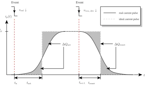
1 Korrektur von Fig. 5
𝐼p
𝑖p(𝑡)
𝑣ref↓ 𝑣vco,div↓
𝑡n 𝑡n+1
𝑡
𝑡set 𝑡reset
Δ𝑄set Δ𝑄reset
Event Event
ideal current pulse real current pulse
Fig. 1. Charge-pump current with slew-rate and delay propagation
from the inputs of the PFD to the output of the charge-pump.
Correspondence to: C. Wiegand
Fig. 5. Charge-pump current with slew-rate and delay propagation
from the inputs of the PFD to the output of the charge-pump.
state signalS(t )is a PWM signal (see Fig. 4). The wider the pulse width is, the bigger is the absolute phase error|ϕe| (de-tected by the PFD). The detectable phase error is limited by the PFD, even if any frequency can be theoretically reached. Thus, a phase error of|ϕe| =2π is equivalent to the occur-rence of two successive falling edges of the refeoccur-rence signal
vref, respectively the output or divider signalvvco,div. Hence, two important state sequences can be identified, where
S6↓= {S−,S−} (8)
and
S6↑= {S+,S+} (9)
are denoted as cycle slips of the down branch (S6↓) respec-tively of the up branch (S6↑). The pull-in process is shown in Fig. 4, where five ranges are emphasized and labeled with
li (i∈ {0,1,2,3,4}). Evidently, if the last cycle slip occurs, the PLL is locked and the absolute phase error remains less than 2π. By considering the logical outputs of the PLL, the transient behaviour can be monitored, without observing the analogue outputs. Assuming that a cycle slip is identified and an overshoot (undershoot) appears subsequently, the PLL is locked. However, the occurrence of an overshoot or an un-dershoot does not imply, that the PLL is locked. If there is no knowledge in terms of a detected cycle slip, an overshoot and an undershoot must be identified. To ensure that the PLL is locked, one of the following state sequences must be de-tected:
S◦= {S↓,S↑} ∨ {S↑,S↓} ∨ {S6↓,S↓} ∨ {S6↑,S↑}. (10) 2.4 Dead-zone
Ideally, the PFD can be modelled as a finite state machine (see Fig. 2), consisting of three states and operating on the triggering edges (falling or rising edges) of the input signal
vref and the divider output signal vdiv (or the VCO output signalvvco when the feedback comprises no divider). Ev-ery state machine can be realized by using flip-flop circuits. equation (5)). It is obvious, that the state signal𝒮(𝑡)is a PWM signal (see. fig 4). The wider the pulse width is, the bigger is the absolute phase error∣𝜑e∣(detected by the PFD). The detectable phase error is limited by the PFD, even if any frequency can be theoretically reached. Thus, a phase error of∣𝜑e∣= 2𝜋is equivalent to the occurrence of two succes-sive falling edges of the reference signal𝑣ref, respectively the output or divider signal𝑣vco,div. Hence, two important state sequences can be identified, where
𝒮∕← ={𝒮−,𝒮−} (8)
and
𝒮∕→ ={𝒮+,𝒮+} (9)
are denoted as cycle slips of the down branch (𝒮
∕←)
respec-tively of the up branch (𝒮
∕→). The pull-in process is shown
in fig. 4, where five ranges are emphasized and labeled with
𝑟𝑖(𝑖∈[0,1,2,3,4]). Evidently, if the last cycle slip occurs,
the PLL is locked and the absolute phase error remains less than2𝜋. By considering the logical outputs of the PLL, the transient behaviour can be monitored, without observing the analogue outputs. Assuming that a cycle slip is identified and an overshoot (undershoot) appears subsequently, the PLL is locked. However, the occurrence of an overshoot or an un-dershoot does not imply, that the PLL is locked. If there is no knowledge in terms of a detected cycle slip, an overshoot and an undershoot must be identified. To ensure that the PLL is locked, one of the following state sequences must be de-tected:
𝒮∘={𝒮↓,𝒮↑} ∨ {𝒮↑,𝒮↓} ∨ {𝒮∕←,𝒮↓} ∨ {𝒮∕→,𝒮↑}. (10)
1.4 Dead-Zone
𝐼p
𝑖p(𝑡)
𝑣ref↓ 𝑣vco,div↓
𝑡n 𝑡n+1
𝑡
𝑡set 𝑡reset
Δ𝑄set Δ𝑄reset
Event Event
ideal current pulse
real current pulse
Fig. 5. Charge-pump current with slew-rate and delay propagation
from the inputs of the PFD to the output of the charge-pump
Ideally, the PFD can be modelled as a finite state machine (see fig. 2), consisting of three states and operating on the triggering edges (falling or rising edges) of the input signal
𝑣ref and the divider output signal𝑣div (or the VCO output signal𝑣vco when the feedback comprises no divider). Ev-ery state machine can be realized by using flip-flop circuits.
Thus, the PFD operates by setting and resetting the flip-flops with the incoming signals𝑣ref and𝑣div(𝑣vco). While a trig-gering edge is identified, the PFD is not able to change the state (the current) instantaneously. Thus, the flip-flop is set by the triggering edge. But, when the phase error is small, the second triggering edge will reset the flip-flop before the signal has been propagated to the output. Correspondingly, the phase error between the incoming signals will not arise at the PFD output (respectively the charge-pump output). Be-side the presented delay propagation from the inputs to out-puts of the PFD, the waveform cannot offer edges with an infinite slope. Thus, a different charge is injected to the loop filters capacitance compared to the ideal charge injection. A schematic waveform is viewed in fig. 5, describing the delay propagation and the charge injection. The aspect of the delay propagation can be modelled introducing virtual states within the state machine. If the charges Δ𝑄set and Δ𝑄reset are equal to zero, the new state machine (see fig. 6) can be used for accurate simulations. IfΔ𝑄set∕= 0andΔ𝑄reset∕= 0, the discrepancy of the charge injection to the loop filter’s capaci-tance can be interpreted as the decrease or the increase of the current pulse integration and therefore this can be modelled as a time delay.
𝜏dn
set 𝜏
up set
𝜏dn
reset 𝜏
up reset
𝑣ref↓
𝑣ref↓ 𝑣ref↓
𝑣ref↓
𝑣ref↓
𝑣vco,div↓
𝑣vco,div↓
𝑣vco,div↓
𝑣vco,div↓
𝑣vco,div↓
Virtual States Virtual States
0 +1
-1
Fig. 6. Modified PFD model describing delay propagation from the
inputs to the output.
The modified PFD model described in fig. 6 represents a sim-ple possibility to include the non-linear characteristic of the dead-zone into the simulation model of equation (3) or into the event-driven modelling techniques (see (Hedayat et al., 1997, 1999; Van Paemel, 1994)).
2 Application and Simulation
Conventional digital lock detection techniques are based on counting methods. These methods are heuristic procedures based on the maximum lock time and the maximum settling time. Because of this, for every application a new counter has to be designed. Additionally, the locking point and set-tling point in time is increasing if the frequency step applied to the system is increasing. Using an identification algorithm of the presented state sequences (see equation (10)), a sim-ple purely digital lock and settling detection circuitry can be
Fig. 6. Modified PFD model describing delay propagation from the
inputs to the output.
Thus, the PFD operates by setting and resetting the flip-flops with the incoming signalsvrefandvdiv (vvco). While a trig-gering edge is identified, the PFD is not able to change the state (the current) instantaneously. Thus, the flip-flop is set by the triggering edge. But, when the phase error is small, the second triggering edge will reset the flip-flop before the signal has been propagated to the output. Correspondingly, the phase error between the incoming signals will not arise at the PFD output (respectively the charge-pump output). Be-side the presented delay propagation from the inputs to out-puts of the PFD, the waveform cannot offer edges with an infinite slope. Thus, a different charge is injected to the loop filters capacitance compared to the ideal charge injection. A schematic waveform is viewed in Fig. 5, describing the de-lay propagation and the charge injection. The aspect of the delay propagation can be modelled introducing virtual states within the state machine. If the charges1Qsetand1Qreset are equal to zero, the new state machine (see Fig. 6) can be used for accurate simulations of the non-linear behaviour. If
1Qset6=0 and 1Qreset6=0, the discrepancy of the charge injection to the loop filter’s capacitance can be interpreted as the decrease or the increase of the current pulse integration and therefore this can be modelled as a time delay.
The modified PFD model described in Fig. 6 represents a simple possibility to include the non-linear characteristic of the dead-zone into the simulation model of Eq. (3) or into the event-driven modelling techniques (see Hedayat et al., 1997, 1999; Van Paemel, 1994).
3 Application and simulation
Conventional digital lock detection techniques are based on counting methods. These methods are heuristic procedures based on the maximum lock time and the maximum settling time. Because of this, for every application a new counter has to be designed. Additionally, the locking point and set-tling point in time is increasing if the frequency step applied to the system is increasing. Using an identification algorithm of the presented state sequences (see Eq. 10), a simple purely digital lock and settling detection circuitry can be developed. The circuit is divided into three subcircuits, identifying the
C. Wiegand et al.: Non-linear behaviour of charge-pump phase-locked loops 165
C. Wiegand et al.: Non-linear behaviour of Charge-Pump Phase-Locked Loops
5
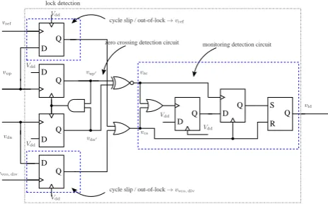
Q R S D Q D Q D D Q D Q Q D Q 𝑉dd 𝑉dd 𝑉dd 𝑉dd 𝑉dd 𝑉dd 𝑣ref
𝑣vco,div
𝑣cs 𝑣zc
cycle slip / out-of-lock→𝑣ref
cycle slip / out-of-lock→𝑣vco,div
𝑣ld 𝑣up
𝑣dn
𝑣up′
𝑣dn′
zero crossing detection circuit monitoring detection circuit lock detection
Fig. 7. Schematic representation of the monitoring circuit based on
the state sequence identification
developed. The circuit is divided into three subcircuits,
iden-tifying the state sequences of equation (3). The cycle slip
(out-of-lock) detection circuit consists of two D-flip-flops
and an OR gate (see fig. 7). Assuming that the UP signal
𝑣
up(resp. the DN signal
𝑣
dn) is true, the occurence of a
ref-erence (resp. output) triggering edge makes the
𝑣
up′(resp.
𝑣
dn′) to be set to one. This situation
{
𝑣
up= 1, 𝑣
up′= 1
}
(resp.
{
𝑣
dn= 1, 𝑣
dn′= 1
}) corresponds to a phase error
larger than
2𝜋
and the PLL is considered as out-of-lock. The
zero crossing detection circuit is depicted in fig. 7. This
cir-cuit is like a conventional tri state PFD, where its outputs are
combined through an exclusive OR gate. It appears that
𝑣
up′(resp.
𝑣
dn′) can be understood as the envelope of
𝑣
up(resp.
𝑣
dn). More precisely, these envelopes are used as inputs of
the exclusive OR gate and thereby make it possible to detect a
digital overshoot or undershoot (zero crossing of the phase).
The lock detection monitoring circuit (see fig. 7) is driven
𝑣ct
l [V ] 𝑣z c [V ] 𝑣c s [V ] 𝑣ld [V ]
Time𝑡[𝜇s]
25 30 35 40 45 50 55 60 65 70 75 0 1 0 1 0 1 0.3 0.35 0.4 0.45 0.5
Fig. 8. Course of events of the important lock detection signals and
the VCO control voltage
𝑣
ctlof a third order CP-PLL.
by the outputs of the cycle slip (out-of-lock) detection circuit
and the zero crossing detection circuit. This monitoring
cir-cuit consists of two D flip-flops, an RS flip-flop and an OR
gate and verifies equation (3). In fig. 8 a Cadence/Spectre
Simulation with
90
nm technology of ST-Microelectronics of
a third order CP-PLL is presented. By means of the proposed
ple possibility to track the transient behaviour of the VCO
control voltage
𝑣
ctl(resp. the output frequency
𝑓
vco) and the
dynamics of the system. The control voltage and the
impor-tant logical outputs of the detection circuitry are depicted in
fig. 8. The lock detection circuit delivers three important
sig-nals: phase zero crossing detection
𝑣
zc, cycle slip detection
𝑣
csand lock detection
𝑣
ld.
3
Conclusions
In this work the non-linear behaviour of a charge-pump
phase-locked loop was characterized and modelled. The
fo-cus was pointed upon the digital phase and frequency
detec-tor, i. e. the switching signature, the dead-zone of the PFD
and the charge-pump. An accurate model of the non-linear
PFD was presented for efficient simulations of mixed signal
systems within event-driven modelling techniques. In
addi-tion, a simple and robust lock detection circuit based on
mon-itoring overshoot/undershoot events and cycle slip
identifica-tion was presented, by using only the digital informaidentifica-tion of
the system (i. e. the input and output signals of the phase and
frequency detector).
Furthermore, the detection circuit can be used to implement
fast locking phase-locked loops with course and fine tuning
elements. Further work will focus on the optimization and an
the further developement of the event-driven and non-linear
modelling and simulation techniques for accurate and
effi-cient design methodologies.
References
Best, R.: Theorie und Anwendungen des Phase-locked Loops,
vde-Verl.; Aarau/Schweiz: ATVerl., 1993.
Daniels, B. and Farrell, R.: Nonlinear Analysis of the 2nd Order
Digital Phase Locked loop, ISSC, Galway, 2008.
Den Dulk, R.: Digital PLL Lock-Detection Circuit, Electronics
Let-ters, 24, 880–882, 1988.
Gardner, F. M.: Phaselock Techniques, John Wiley & Sins, Inc.,
1966.
Gardner, F. M.: Charge-Pump Phase-Lock Loops,
Communica-tions, IEEE Transactions on, 28, 1849–1858, 1980.
Hedayat, C. D., Hachem, A., Leduc, Y., and Benbassat, G.:
High-Level Modeling Applied to the Second-Order Charge-Pump PLL
Circuit, Texas Instruments Technical Journal, 14, 1997.
Hedayat, C. D., Hachem, A., Leduc, Y., and Benbassat, G.:
Model-ing and Characterization of the Third Order Charge-Pump PLL:
A Fully Event-Driven Approach, Analog Integrated Circuits and
Signal Processing, 19, 24–45, 1999.
Shu, K. and Sanchez-Sinencio, E.: CMOS PLL Synthesizers:
Anal-ysis and Design, Springer, 2005.
Van Paemel, M.: Analysis of a Charge-Pump PLL: A New Model,
Communications, IEEE Transactions on, 42, 2490–2498, doi:10.
1109/26.297861, 1994.
Wolaver, D. H.: Phase-Locked Loop Circuit Design, Advanced
Ref-erence Series & Biophysics and Bioengineering Series,
Engle-Fig. 7. Schematic representation of the monitoring circuit based on
the state sequence identification.
state sequences of Eq. (3). The cycle slip (out-of-lock) de-tection circuit consists of two D-flip-flops and an OR gate (see Fig. 7). Assuming that the UP signalvup(resp. the DN signalvdn) is true, the occurence of a reference (resp. output) triggering edge makes thevup0 (resp.vdn0) to be set to one.
This situation
vup=1,vup0=1 (resp. {vdn=1,vdn0=1})
corresponds to a phase error larger than 2π and the PLL is considered as out-of-lock. The zero crossing detection cir-cuit is depicted in Fig. 7. This circir-cuit is like a conventional tri state PFD, where its outputs are combined through an ex-clusive OR gate. It appears thatvup0 (resp.vdn0) can be
un-derstood as the envelope ofvup(resp.vdn). More precisely, these envelopes are used as inputs of the exclusive OR gate and thereby make it possible to detect zero crossing of the phase error (digital overshoot or undershoot).
The lock detection monitoring circuit (see Fig. 7) is driven by the outputs of the cycle slip (out-of-lock) detection circuit and the zero crossing detection circuit. This monitoring cir-cuit consists of two D flip-flops, an RS flip-flop and an OR gate and verifies Eq. (3). In Fig. 8 a Cadence/Spectre Sim-ulation with 90nm technology of ST-Microelectronics of a third order CP-PLL is presented. By means of the proposed lock detection circuit, the digital information delivers a sim-ple possibility to track the transient behaviour of the VCO control voltagevctl(resp. the output frequencyfvco) and the dynamics of the system. The control voltage and the impor-tant logical outputs of the detection circuitry are depicted in Fig. 8. The lock detection circuit delivers three important sig-nals: phase zero crossing detectionvzc, cycle slip detection vcsand lock detectionvld.
4 Conclusions
In this work the non-linear behaviour of a charge-pump phase-locked loop was characterized and modelled. The fo-cus was pointed upon the digital phase and frequency detec-tor, i.e. the switching signature, the dead-zone of the PFD and
C. Wiegand et al.: Non-linear behaviour of Charge-Pump Phase-Locked Loops
5
Q R S D Q D Q D D Q D Q Q D Q 𝑉dd 𝑉dd 𝑉dd 𝑉dd 𝑉dd 𝑉dd 𝑣ref
𝑣vco,div
𝑣cs 𝑣zc
cycle slip / out-of-lock→𝑣ref
cycle slip / out-of-lock→𝑣vco,div
𝑣ld 𝑣up
𝑣dn
𝑣up′
𝑣dn′
zero crossing detection circuit monitoring detection circuit lock detection
Fig. 7. Schematic representation of the monitoring circuit based on the state sequence identification
developed. The circuit is divided into three subcircuits,
iden-tifying the state sequences of equation (3). The cycle slip
(out-of-lock) detection circuit consists of two D-flip-flops
and an OR gate (see fig. 7). Assuming that the UP signal
𝑣
up(resp. the DN signal
𝑣
dn) is true, the occurence of a
ref-erence (resp. output) triggering edge makes the
𝑣
up′(resp.
𝑣
dn′) to be set to one. This situation
{
𝑣
up= 1, 𝑣
up′= 1
}
(resp.
{
𝑣
dn= 1, 𝑣
dn′= 1
}
) corresponds to a phase error
larger than
2𝜋
and the PLL is considered as out-of-lock. The
zero crossing detection circuit is depicted in fig. 7. This
cir-cuit is like a conventional tri state PFD, where its outputs are
combined through an exclusive OR gate. It appears that
𝑣
up′(resp.
𝑣
dn′) can be understood as the envelope of
𝑣
up(resp.
𝑣
dn). More precisely, these envelopes are used as inputs of
the exclusive OR gate and thereby make it possible to detect a
digital overshoot or undershoot (zero crossing of the phase).
The lock detection monitoring circuit (see fig. 7) is driven
𝑣ctl
[V
]
𝑣zc
[V
]
𝑣cs
[V
]
𝑣ld
[V
]
Time𝑡[𝜇s]
25 30 35 40 45 50 55 60 65 70 75
0 1 0 1 0 1 0.3 0.35 0.4 0.45 0.5
Fig. 8. Course of events of the important lock detection signals and the VCO control voltage𝑣ctlof a third order CP-PLL.
by the outputs of the cycle slip (out-of-lock) detection circuit
and the zero crossing detection circuit. This monitoring
cir-cuit consists of two D flip-flops, an RS flip-flop and an OR
gate and verifies equation (3). In fig. 8 a Cadence/Spectre
Simulation with
90
nm technology of ST-Microelectronics of
a third order CP-PLL is presented. By means of the proposed
lock detection circuit, the digital information delivers a
sim-ple possibility to track the transient behaviour of the VCO
control voltage
𝑣
ctl(resp. the output frequency
𝑓
vco) and the
dynamics of the system. The control voltage and the
impor-tant logical outputs of the detection circuitry are depicted in
fig. 8. The lock detection circuit delivers three important
sig-nals: phase zero crossing detection
𝑣
zc, cycle slip detection
𝑣
csand lock detection
𝑣
ld.
3
Conclusions
In this work the non-linear behaviour of a charge-pump
phase-locked loop was characterized and modelled. The
fo-cus was pointed upon the digital phase and frequency
detec-tor, i. e. the switching signature, the dead-zone of the PFD
and the charge-pump. An accurate model of the non-linear
PFD was presented for efficient simulations of mixed signal
systems within event-driven modelling techniques. In
addi-tion, a simple and robust lock detection circuit based on
mon-itoring overshoot/undershoot events and cycle slip
identifica-tion was presented, by using only the digital informaidentifica-tion of
the system (i. e. the input and output signals of the phase and
frequency detector).
Furthermore, the detection circuit can be used to implement
fast locking phase-locked loops with course and fine tuning
elements. Further work will focus on the optimization and an
the further developement of the event-driven and non-linear
modelling and simulation techniques for accurate and
effi-cient design methodologies.
References
Best, R.: Theorie und Anwendungen des Phase-locked Loops, vde-Verl.; Aarau/Schweiz: ATVerl., 1993.
Daniels, B. and Farrell, R.: Nonlinear Analysis of the 2nd Order Digital Phase Locked loop, ISSC, Galway, 2008.
Den Dulk, R.: Digital PLL Lock-Detection Circuit, Electronics Let-ters, 24, 880–882, 1988.
Gardner, F. M.: Phaselock Techniques, John Wiley & Sins, Inc., 1966.
Gardner, F. M.: Charge-Pump Phase-Lock Loops, Communica-tions, IEEE Transactions on, 28, 1849–1858, 1980.
Hedayat, C. D., Hachem, A., Leduc, Y., and Benbassat, G.: High-Level Modeling Applied to the Second-Order Charge-Pump PLL Circuit, Texas Instruments Technical Journal, 14, 1997.
Hedayat, C. D., Hachem, A., Leduc, Y., and Benbassat, G.: Model-ing and Characterization of the Third Order Charge-Pump PLL: A Fully Event-Driven Approach, Analog Integrated Circuits and Signal Processing, 19, 24–45, 1999.
Shu, K. and Sanchez-Sinencio, E.: CMOS PLL Synthesizers: Anal-ysis and Design, Springer, 2005.
Van Paemel, M.: Analysis of a Charge-Pump PLL: A New Model, Communications, IEEE Transactions on, 42, 2490–2498, doi:10. 1109/26.297861, 1994.
Wolaver, D. H.: Phase-Locked Loop Circuit Design, Advanced Ref-erence Series & Biophysics and Bioengineering Series, Engle-wood Cliffs, New Jersey 07632: Prentice Hall,, 1991.
Fig. 8. Course of events of the important lock detection signals and
the VCO control voltagevctlof a third order CP-PLL.
the charge-pump. An accurate model of the non-linear PFD was presented for efficient simulations of mixed signal sys-tems within event-driven modelling techniques. In addition, a simple and robust lock detection circuit based on moni-toring zero crossing (overshoot/undershoot) events and cycle slip identification was presented, by using only the digital in-formation of the system (i.e. the input and output signals of the phase and frequency detector).
Furthermore, the detection circuit can be used to imple-ment fast locking phase-locked loops with course and fine tuning elements. Further work will focus in the optimization and an the further developement of the event-driven and non-linear modelling and simulation techniques for accurate and efficient design methodologies.
References
Best, R.: Theorie und Anwendungen des Phase-locked Loops, vde-Verl.; Aarau/Schweiz: ATVerl., 1993.
Daniels, B. and Farrell, R.: Nonlinear Analysis of the 2nd Order Digital Phase Locked loop, ISSC, Galway, 2008.
Den Dulk, R.: Digital PLL Lock-Detection Circuit, Electronics Let-ters, 24, 880–882, 1988.
Gardner, F. M.: Phaselock Techniques, John Wiley & Sins, Inc., 1966.
Gardner, F. M.: Charge-Pump Phase-Lock Loops, Communica-tions, IEEE Transactions on, 28, 1849–1858, 1980.
Hedayat, C. D., Hachem, A., Leduc, Y., and Benbassat, G.: High-Level Modeling Applied to the Second-Order Charge-Pump PLL Circuit, Texas Instruments Technical Journal, 14, 1997. Hedayat, C. D., Hachem, A., Leduc, Y., and Benbassat, G.:
Model-ing and Characterization of the Third Order Charge-Pump PLL: A Fully Event-Driven Approach, Analog Integrated Circuits and Signal Processing, 19, 24–45, 1999.
Shu, K. and Sanchez-Sinencio, E.: CMOS PLL Synthesizers: Anal-ysis and Design, Springer, 2005.
Van Paemel, M.: Analysis of a Charge-Pump PLL: A New Model, Communications, IEEE Transactions on, 42, 2490–2498, doi:10. 1109/26.297861, 1994.
Wolaver, D. H.: Phase-Locked Loop Circuit Design, Advanced Ref-erence Series & Biophysics and Bioengineering Series, Engle-wood Cliffs, New Jersey 07632: Prentice Hall, 1991.