Fuzzy Logic Controller based Interleaved PFC Power Factor
Correction with Output Voltage
B.Himabindu
&
M.Purushothm
1
PG Scholar, SHREE Institute of Technical Education, Tirupati, Andhra Pradesh, India.
2Associate.Prof & HOD, SHREE Institute of Technical Education, Tirupati, Andhra Pradesh, India.
Abstract: A power factor Correction (PFC) usually serves as the first stage of active two-stage AC/DC converters in a variety of applications including inductive heating systems, wireless charging systems, and onboard chargers for plug-in electric vehicles (PEVs). Conventionally, boost-type PFCs are utilized to regulate the DC-link voltage at a fixed voltage; however, a variable DC-link voltage can enhance the overall efficiency of the converters. In this paper, Fuzzy Logic Control based interleaved PFC converter with coupled inductors is proposed as the PFC stage for two-stage AC/DC converters. The converter is designed to operate in discontinuous conduction mode (DCM) in order to achieve soft switching for switches and diodes. The directly coupled inductors are utilized to reduce the number of magnetic components and decrease the input current ripple. A 500W FLC Based interleaved PFC Converter is designed to verify the benefits of this converter. The MATLAB/SIMULINK results show that the converter can maintain high efficiency over a wide range of DC-link voltage and input power factor maintaining approximately at unity.
Keywords—Power factor Correction (PFC), single ended
primary inductor converter (PFC), discontinuous
conduction mode (DCM), coupled inductors, interleaved converter, Fuzzy Logic Control (FLC).
I. INTRODUCTION
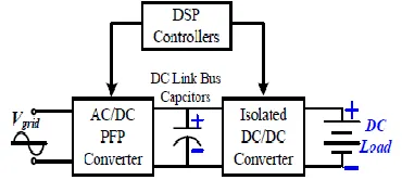
To improve the power quality of the gird, high power factor (PF) and low total harmonics distortion (THD) are required for the grid-connected AC/DC converters. Nowadays, two-stage active AC/DC converters have been widely used in a variety of applications such as onboard chargers for plug-in electric vehicles (PEVs), inductive heating systems, and wireless charging systems [1]-[3]. The two-stage AC/DC converters are typically composed of a PFP stage followed by an isolated DC/DC stage, as shown in Fig. 1 [1]. A DC/DC resonant converter is usually selected as the second stage due to its attractive features such as soft switching, galvanic isolation, and high efficiency near resonant frequency. AC/DC PFP Converter Vgrid Isolated DC/DC Converter DC Load DC Link Bus Capcitors DSP Controllers
Fig. 1. Typical structure of two-stage active AC/DC converters.
The objective of PFP stage is to improve power quality and reduce harmonic contamination. The topology for the PFP stage is a diode bridge followed by a boost-type converter [1]. Although the boost-type PFP converters can provide efficiencies over 98% [4]-[5], the overall efficiency of the two-stage converter is reduced significantly if the second-stage resonant converter cannot operate near the resonant frequency.
Fig. 2. Two-stage battery charger system. Additionally, the boost-type PFPs are not the most suitable topologies for inductive heating applications, where the high frequency AC magnetic field should be generated to deliver power over a distance by a subsequent resonant converter stage [3]. A wide output voltage variation is required in this application due to a need for variable power levels for heating. Similar to onboard charger application, a fixed DC-link voltage would result in lower overall efficiency particularly in light loads by using a resonant DC/DC converter stage controlled by pulse frequency modulation. For such applications, a PFP stage capable of providing a wide regulated DC-link voltage, such as a single-ended primary-inductor converter (PFC) PFP, can improve the overall efficiency of the systems to a great extent.
The PFC topology, shown in Fig. 3, has been investigated as the PFP in AC/DC converters in various applications including standalone photovoltaic systems and LED lighting systems [14]-[23]. In a PFC PFP, the output voltage can be either higher or lower than the input voltage. The voltage and current stresses of diodes and switches, in a traditional PFC converter, are much higher than a boost-type topology at the same power level. Thus, the traditional PFC topology is not widely used for high power applications [24]. The bridgeless PFC PFP converters have been investigated to reduce the conduction loss of the diode bridge in [15]-[18]. However, the voltage and current stresses of switches are not reduced, and the power level is usually limited to less than 150W, due to voltage and current limitations of switches in the orders of 300V and 10A, respectively. In addition, in the continuous conduction mode (CCM), the PFC converters have large hard-switching losses, especially in high frequency operation. Therefore, the efficiencies are low for a traditional PFC converter operated in CCM. In [3], the power level is increased by interleaving two PFC converters. However, this topology is constructed by directly paralleling two traditional PFC converters, and consequently the input current ripple is large in discontinuous conduction mode (DCM) operation.
Fig. 3. Traditional PFC PFP converter.
In this paper, a two-phase interleaved PFC AC/DC converter with coupled inductors is proposed to serve as the PFP stage with a wide range of output DC-link voltage. Its topology is shown in Fig. 4. The input power is shared evenly between two phases to reduce the current stresses of the switches and diodes; and consequently, the power level can be increased. Since the CCM operation causes large switching losses, the DCM operation is selected to enable soft switching. The ZVS can be realized for the MOSFET’s to reduce the switching losses, while the ZCS can be realized for diodes, D1 and D2, to eliminate reverse recovery losses [14]. In order to reduce the number of magnetic components, the corresponding inductors in two phases are directly coupled. The input current ripple could be significantly reduced through proper design of the coupled inductors.
Fig. 4. Proposed interleaved PFC PFP converter. This paper is organized as follows. The principle of operation is presented in Section II. The theoretical analyses are elaborated in Section III. Furthermore, experimental results of a 500W prototype are demonstrated in Section IV for validation of the analyses. Finally, Section V concludes the manuscript.
II OPERATION PRINCIPLE
In Fig. 4, the rectified voltage after the diode bridge can be modeled as an equivalent variable DC source
Vg. Assuming that the DC-link capacitor CDC and two middle capacitors C1, C2 are large enough and their voltage ripples are negligible compared with their steady-state voltages. The output capacitor can be modeled with an equivalent DC source Vo. Since the middle capacitors C1
modeled as the equivalent variable DC source Vg [24], as shown in Fig. 5.
The analyses are separated into the higher output voltage case and the lower output voltage case as the output voltage of a PFC converter can be either higher or lower than the input peak voltage. These two cases are analyzed in this section using the derived equivalent model.
Fig 5. Equivalent circuit of the proposed interleaved PFC converter.
A. Lower Output Voltage Case
The output voltage of PFP stage can be lower than the input peak voltage. In DCM operation, the duty cycle is less than 0.5, and it is also less than the duty cycle derived in CCM operation with the same output voltage [24].
Fig 6. Typical waveforms of the interleaved PFC converter in DCM.
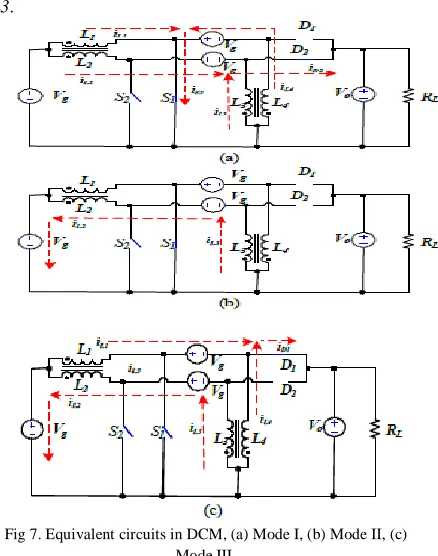
The typical waveforms of the converter in DCM are shown in Fig. 6, in which there are six modes in one switching cycle. There are three modes in each of the positive and the negative half cycle operations. Here, only three modes in positive half cycle are analyzed due to the symmetry of operation. The equivalent circuit for each mode is shown in Fig. 7.
In this two-phase interleaved topology, the corresponding inductors in two phases are coupled using the same cores with the same coupling coefficients. The inductor L1 is coupled with L2, while the inductor L3 is coupled with inductor L4. These four inductors have the same self-inductances and mutual inductances. In each operation mode, the voltages across inductors L1 and L4
are the same in each operation mode. Thus, the inductor
currents iL1 and iL4 have similar waveforms as shown in Fig. 6. Similar waveforms are valid for inductors L2 and
L3.
Fig 7. Equivalent circuits in DCM, (a) Mode I, (b) Mode II, (c) Mode III.
1) Mode I (t0-t1):
In this mode, as shown in Fig. 7(a), the switch S1 is on, while the switch S2 is off. The diode D1 is off, and diode
D2 is on. The voltages across both inductors L1 and L4 are
Vg. Therefore, the inductor currents iL1 and iL4 increase at the same rates. The current through S1, iS1, is the sum of the inductor currents iL1 and iL4. Meanwhile, voltages across both inductors L2 and L3 are −Vo. Thus, the inductor currents iL2 and iL3 decrease at the same rates, and the current through diode D2, iD2, is the sum of these two inductor currents.
As the inductors L1 and L2 are directly coupled, the core flux is affected by both inductor currents iL1 and iL2. The mutual inductance, M, is defined as,
𝑀 = √𝐿12. 𝐿21 … … (1)
where, L12 is the mutual inductance induced by the inductor current iL1 in inductor L2, and L21 is the mutual inductance induced by the inductor current iL2 in inductor
L1. Since the mutual inductance of inductors L1 and L2 are the same, the mutual inductance M has the same value as
L12 and L21. Additionally, the coupling coefficient, k, is defined as,
𝐾 = 𝑀
√𝐿1. 𝐿2
where, L1 and L2 are self-inductances of the first coil and the second coil.
The voltages and currents of the mutually coupled inductors can be expressed as,
…. (3)
…… (4) Eq. (3) and Eq. (4) can be rearranged as,
(5)
(6)
Seen from the Fig. 6, the inductor current iL2 decreases all the time and changes the flowing direction in this mode. The current through diode D2, iD2, keeps on decreasing. The variations of inductor currents, ΔiL1 and ΔiL2, can be expressed as
(7)
Where, T is the switching period, and D'T is the time interval between t0 and t1.
2) Mode II (t1-t2):
At t1, the current through diode D2, iD2, which is the sum of inductor currents iL2 and iL3, drops to zero. Then, the diode turns off with ZCS. Meantime, the inductor currents
iL3 and iL2 flow in a loop composed of the inductor L3, the capacitor C2, the inductor L2, and the equivalent voltage source Vg, as shown in Fig. 7(b).
The variations of inductor currents iL3 and iL2
are the same due to the same voltages across inductors L3
and L2. In addition, the average current of iL3 is higher than the average current of iL2 [17]. Thus, at t1, when the inductor currents iL3 and iL2 drop to minimum, the inductor current iL3 is higher than iL2 with iL3 as positive value and iL2 as negative value, as shown in Fig. 6. The current flows from inductor L3 to inductor L2 in the aforementioned loop containing inductors L3 and L2. Assuming that the resistances of inductors and capacitors in this loop are negligible, the loop current remains constant from t1 to t2, as expressed in Eq. (9).
(8)
The inductor current iL1 changes with a higher rate in comparison to Mode I as expressed in Eq. (10). The current of coupled inductor L2 is constant, and only sets the flux bias.
(9)
Consequently, the variation of inductor current, ΔiL1, can be expressed as,
(10)
Where, D is the duty cycle. Similar expressions are valid for the inductor L4.
3) Mode III (t2-t3):
As shown in Fig. 7(c), both switches are off in this mode. The diode D2 is off, while the diode D1 turns on. The constant current flows in the aforementioned loop consisting of inductors L2 and L3. The inductor currents
iL1 and iL4 decrease from maximum values, and the sum of them flows through the diode D1. The voltages across both inductors L1 and L4 are −Vo. The inductor current iL1
decreases at a rate expressed as,
(11)
Consequently, the variation of inductor current, ΔiL1, can be shown as,
(12) Similar expressions are applicable for the inductor L4.
B. Higher Output Voltage Case
The waveforms of higher output voltage case are similar to those of lower output voltage case. In DCM, the operation principles of higher output voltage case are similar to those of lower output voltage case. In a switching cycle, there are six modes, among which only three modes are analyzed due to the symmetry of operation.
1) Mode I:
The inductor currents iL1 and iL2 increase simultaneously at small rates. Similar to the lower output voltage case, the slew rate of inductor current iL1 and iL2 are expressed as,
(14)
Thus, the inductor current variations, ΔiL1 and ΔiL2, can be expressed as,
(15)
(16) Since the L3 and L4 have the same inductance values as L1
and L2, similar equations can be derived for the inductor currents iL3 and iL4.
2) Mode II:
(17)
(18)
Similar to the lower output voltage case, the slew rate of inductor current iL1 can iL2 are expressed as,
(19)
(19)
The inductor current iL3 decreases and changes the direction in this mode. The current through diode, D2, keeps on decreasing. 𝐷′𝑇 is the time interval between the diode D2 turn-on and turn-off. The variations of inductor currents, ΔiL1 and ΔiL2, can be expressed as,
(20)
(21)
3) Mode III (t2-t3):
At t2, the current through diode, D2, drops to zero. Then, the diode turns off with ZCS. Meanwhile, the currents of inductors L2 and L3 circulate in a loop composed of the inductor L3, the capacitor C2, the inductor L2, and the equivalent voltage source Vg. The constant current flows from inductor L2 to inductor L3. Thus, Eq. (22) can be obtained as,
The inductor current iL1 changes with a higher rate in comparison to Mode I as expressed in Eq. (23). The current of coupled inductor L2 is constant, and only sets the flux bias.
(22)
Therefore, the inductor current variations, ΔiL1, can be expressed as,
(23)
Similar expressions are valid for inductor L4. III. ANALYSIS OF THE PROPOSED PFP
TOPOLOGY
Based on the operation principles for higher output voltage and lower output voltage cases, the detailed analysis can be conducted to set the critical parameters of power components and to assess the circuit performance. Relevant expressions are derived in this section. The analyses are based on the assumption of unity power factor and a constant output voltage due to a large output filter capacitance.
A. Reduced Input Current Ripple by Coupled Inductors
In this section, the input current ripple is calculated in DCM operation. Although the two PFC converters work in DCM operation individually, the input current maintains CCM features with a small input current ripple.
As shown in Fig. 6, from t0 to t1, the current of
From t1 to t2, the current of L2 becomes constant, and the current of L1 increases at a different rate. The input current variation, Δi2, is expressed as,
The input current ripple is the sum of the two variations,
Δi1 and Δi2. Thus
where, a and b are the weighted coefficients
where, L = L1 = L2.
The coefficient a is much smaller than coefficient
b, and consequently the input current ripple is mostly determined by second term based on Eq. (27). Thus, the input current becomes larger as the converter works in deeper DCM operation. In order to reduce the input current ripple, the converter should operate under DCM in close proximity to boundary conduction mode (BCM). When D’ becomes equal to D, the converter works in BCM with minimum input current ripple. Compared with the input current ripples of traditional PFC and interleaved PFC with non-coupled inductors, the input current ripple is significantly reduced. The expressions for input current ripples are listed in Table I.
TABLE I
INPUT CURRENT RIPPLES OF THREE TOPOLOGIES
VI. FUZZY LOGIC CONTROL
L. A. Zadeh presented the first paper on fuzzy set theory in 1965. Since then, a new language was developed to describe the fuzzy properties of reality, which are very difficult and sometime even impossible to be described using conventional methods. Fuzzy set theory has been widely used in the control area with some application to power system [5]. A simple fuzzy logic control is built up by a group of rules based on the human knowledge of system behavior. Matlab/Simulink simulation model is built to study the dynamic behavior of converter. Furthermore, design of fuzzy logic controller can provide
desirable both small signal and large signal dynamic performance at same time, which is not possible with linear control technique. Thus, fuzzy logic controller has been potential ability to improve the robustness of compensator. The basic scheme of a fuzzy logic controller is shown in Fig.3 and consists of four principal components such as: a fuzzy fication interface, which converts input data into suitable linguistic values; a knowledge base, which consists of a data base with the necessary linguistic definitions and the control rule set; a decision-making logic which, simulating a human decision process, infer the fuzzy control action from the knowledge of the control rules and linguistic variable definitions; a de-fuzzification interface which yields non fuzzy control action from an inferred fuzzy control action [10].
Fig.8. Block diagram of the Fuzzy Logic Controller (FLC).
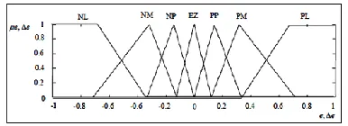
Fig.9 Membership functions for Input, Change in input, Output.
Rule Base: the elements of this rule base table are determined based on the theory that in the transient state, large errors need coarse control, which requires coarse in-put/output variables; in the steady state, small errors need fine control, which requires fine input/output variables. Based on this the elements of the rule table are obtained as shown in Table 1, with „Vdc‟ andVdc-ref as inputs. In this
section, a 500W interleaved PFC converter with coupled inductors is designed to validate the theoretical analysis. The experiments are conducted to validate the advantages of proposed topology.
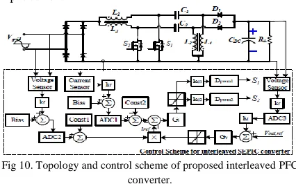
A. Control Scheme
carrier signals of switches S1 and S2 have 180o phase shift. The control is implemented in a DSP controller. In the voltage control loop, the voltage error between the output voltage and its reference voltage is fed to the voltage-loop PI controller, Gv, to generate the reference signal of the input current.
Fig 10. Topology and control scheme of proposed interleaved PFC converter.
Then, the current error between this generated current reference and input current is fed to current-loop PI controller, Gi, to adjust the duty ratio for switches S1 and
S2.
B. Design of Critical Components
1) Intermediate capacitor
In a PFC converter, the intermediate capacitor has two tasks: (i) to keep a constant voltage in a switching period; and (ii) to follow the variation of the input voltage [14]. Thus, the selection of this capacitor is constrained by the grid frequency, fl, and the switching frequency, fs. The resonant frequency of the intermediate capacitor and the input inductor has to be much larger than the line frequency to avoid the oscillation of the input current. On the other hand, this resonant frequency has to be much lower than the switching frequency to reduce the voltage ripple of the intermediate capacitor. The large voltage ripple causes large power loss on the intermediate capacitor, which reduces the efficiency and reduces the life of the intermediate capacitor.
(23)
In the experiment, the operation frequency of the PFP, 𝑓𝑠, is set as 150kHz, and the 𝑓𝑟 is set as 10kHz. Thus, the intermediate capacitor can be selected as 1μF.
2) Inductors and coupling coefficient
A proper coupling coefficient for the entire range of output DC-link voltage is critical for the performance of the circuit. A coupling coefficient much higher than the
minimum value, kmin, increases the input current ripple. On the other hand, a low coupling coefficient increases the size of the coupled inductor because a larger magnetic core would be needed without significantly increasing coil turns.
In order to select a proper coupling coefficient, the inductance of coupled inductors should be taken into consideration. On one hand, the inductance cannot be too small. As shown in Table II, the kminvalue of the higher output voltage case is much smaller than that of the lower output voltage case given a small inductance L2. However, the kmin should not be too much different for these two cases. Otherwise, the converter would enter deep DCM in higher output voltage case, resulting in significantly increased input current ripple in this case. On the other hand, the inductance L2 cannot be too large because the coil turns increase largely for higher inductance L2, resulting in much larger size of the coupled inductors. According to Table II, the inductance of 400uH with a minimum coupling coefficient of 0.8391 is selected for both coupled inductors. To ensure the DCM operation, the coupling coefficient is chosen as 0.85.
To implement the coupled inductor, the ETD44 core is selected, and Litz wire is adopted to build the coils due to the high switching frequency. Coils of both coupled-inductors have 24 turns. The air gap is tuned to be 0.3mm to set the coupling coefficient as 0.85. As the voltage stress between the two coupled-inductors is really high, a large air gap (5mm) is incorporated between the two coils. An image of the coupled inductor, designed for this application, is shown in Fig. 8.
The parameters of all the components in the two-phase interleaved PFC converter with coupled inductor s are listed in Table II.
TABLE IV
DESIGN PARAMETERS OF THE CONVERTER
IV MATLAB SIMULINK RESULTS
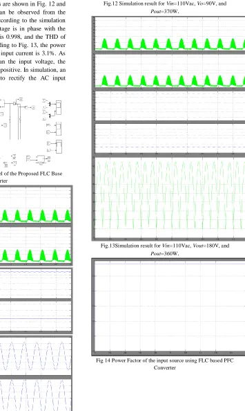
is 110Vac. The simulation results are shown in Fig. 12 and Fig. 13. The DCM operation can be observed from the inductors current waveforms. According to the simulation results in Fig. 12, the input voltage is in phase with the input current. The power factor is 0.998, and the THD of the input current is 3.5%. According to Fig. 13, the power factor is 0.996, and THD of the input current is 3.1%. As the output voltage is higher than the input voltage, the currents of L1 and L2 are mostly positive. In simulation, an ideal diode bridge is utilized to rectify the AC input voltage.
Fig 11 MATLAB SIMULINK Model of the Proposed FLC Base PFC Converter
Fig.12 Simulation result for Vin=110Vac, Vo=90V, and
Pout=370W.
Fig.13Simulation result for Vin=110Vac, Vout=180V, and
Pout=360W.
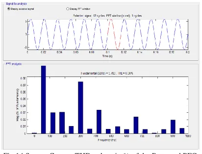
Fig 14 Source Current THD values in % of the Proposed PFC Converter with PI Controller
Fig 14 Source Current THD values in % of the Proposed PFC Converter with Fuzzy Logic Controller
V. CONCLUSION
This paper proposed a novel Fuzzy Logic Control based interleaved two phases PFC Converter with inductors directly coupled. The directly coupled inductors can reduce the number of magnetic components, decrease the input current ripple. The key circuit and design features are summarized as follows. The power level of PFC is improved by interleaving two AC/DC converters, the voltage and current stresses of the diodes and switches are largely reduced, improving the power level up to 500W. High efficiency, low harmonics is maintained over a wide range of DC-link voltage. The converter is designed to operate in DCM in order to achieve ZVS for switches and ZCS for diodes. The input current ripple is reduced by properly designing the coupled inductors. The inductance and coupling coefficient are carefully selected for the coupled inductors to ensure the DCM operation in close proximity to BCM operation over the wide range of DC-link voltage. A 500W prototype is built to validate the advantages of this proposed PFC. The MATLAB SIMULINK results show the proposed interleaved FLC based PFC Converter can provide a wide output DC-Link
voltage from 90V to 190V at 110Vac input voltage, and the efficiency is over 96% at 500W over a wide range of DC-link voltage with power factor over 0.95845.
REFERENCES
[1] Singh, Bhim, Brij N. Singh, Ambrish Chandra, Kamal Al-Haddad, AshishPandey, and Dwarka P. Kothari. "A review of single-phase improved power quality AC-DC converters", IEEE Trans. Ind. Electron., vol. 50, no. 5, pp. 962-981, 2003.
[2] Musavi, Fariborz, Wilson Eberle, and William G. Dunford, "A high-performance single-phase bridgeless interleaved PFC converter for plug-in hybrid electric vehicle battery chargers," IEEE Trans. Ind. Appl., vol.47, no.4, pp. 1833-1843, Apr. 2011.
[3] Chen, Rui, and Jih-Sheng Lai, "Analysis and design of DCM PFC PFC with adjustable output voltage," in Proc. IEEE APEC, 2015, pp. 477-484.
[4] Fei Zhang and JianpingXu, “A Novel PCCM Boost PFC Converter With Fast Dynamic Response”, IEEE Trans. Ind. Electron., vol. 58, no. 9, pp. 4207-216, Sept. 2011.
[5] A. Khaligh and S. Dusmez, "Comprehensive topological analysis of conductive and inductive charging solutions for plug-in electric vehicles," IEEE Trans. Veh.Technol., vol.61, no.8, pp. 3475-3489, Aug. 2012. [6] F. Musavi, M. Craciun, D.S. Gautam, W. Eberle, and W.G. Dunford, “An LLC resonant DC–DC converter for wide output voltage range battery charging applications,”
IEEE Trans. Power Electron., vol. 28, no. 12, pp. 5437-5445, 2013.
[7] S. Dusmez, , and A. Khaligh, "Generalized technique of compensating low-frequency component of load current with a parallel bidirectional DC/DC converter," IEEE Trans. Power Electron., vol. 29, no. 11, pp. 5892-5904, Nov. 2014.
[8] H. Wang, S. Dusmez, and A. Khaligh, "Maximum Efficiency Point Tracking Technique for LLC Based PEV Chargers through Variable DC Link Control," IEEE Trans. Ind. Electron., vol. 61, no. 11, pp. 6041-6049, Nov. 2014. [9] J. Deng, S. Li, S. Hu, C. C. Mi, and R. Ma, “Design Methodology of LLC Resonant Converters for Electric Vehicle Battery Chargers,” IEEE Trans. Veh. Technol., vol. 63, no. 4, pp. 1581–1592, Apr. 2014.
[10] W. Guo, H. K. Bai, G. Szatmari-voicu, A. Taylor, J. Patterson, and J. Kane, “A 10kW 97%-efficiency LLC Resonant DC/DC Converter with Wide Range of Output Voltage for the Battery Chargers in Plug-in Hybrid Electric Vehicles,” in Proc. IEEE ITEC, 2012, pp.1-4.
for wide battery voltage range," IEEE Trans. Veh. Technol.,
vol. 63, no. 4, pp. 1603-1613, Apr. 2014.
[12] S. Dusmez, and A. Khaligh, “A compact and integrated multifunctional power electronic interface for plug-in electric vehicles,” IEEE Trans. Power Electron.,
vol. 28, no. 12, pp.5690-5701, Dec. 2013.
[13] S. Dusmez, , and A. Khaligh, "A charge-nonlinear-carrier-controlled reduced-part single-stage integrated power electronics interface for automotive applications,"
IEEE Trans. Veh. Technol., vol. 63, no. 3, pp. 1091-1103, Mar. 2014.
[14] LyrioSimonetti, DomingosSavio, Javier Sebastian, and Javier Uceda, "The discontinuous conduction mode PFC and Cuk power factor preregulators: analysis and design,"
IEEE Trans. Ind. Electron., vol.44, no.5, pp. 630-637, May 1997.
[15] Mahdavi, Mohammad, and HoseinFarzanehfard. "Bridgeless PFC PFC rectifier with reduced components and conduction losses," IEEE Trans. Ind. Electron., vol.58, no.9, pp. 4153-4160, Sept.2011.
[16] Jae-Won Yang and Hyun-Lark Do, “Bridgeless PFC Converter With a Ripple-Free Input Current”, IEEE Trans. Power Electron., vol. 28, no. 7, pp. 3388–3394, Jul. 2013. [17] Ahmad J. Sabzali, Esam H. Ismail, Mustafa A. Al-Saffar and Abbas A. Fardoun, "New Bridgeless DCM PFC and Cuk PFC Rectifiers With Low Conduction and Switching Losses," IEEE Trans. Ind. Appl., vol.47, no.2, pp. 873-881, Mar. 2011.
Ms.B.Himabindu is pursuing her Master of Technology in Power Electronics, EEE Department, SHREE Institute of Technical Education, Tirupati, and Andhra Pradesh, India.