Available online:
http://edupediapublications.org/journals/index.php/IJR/
P a g e | 757Design and Simulation of PV Based Multi Level Inverter to Reduce
Leakage Current FED Induction Motor Drive
JAREENA M-tech Student Scholar Department of Electrical & Electronics
Engineering,
Sri Indu Institute of Engineering & T echnology; Hyderabad .T elangana, India.
K. MURALI Assistant Professor Department of Electrical & Electronics
Engineering,
Sri Indu Institute of Engineering & T echnology. Hyderabad, T elangana, India.
Dr. I. SAT YANARAYANA
PRINCIPAL
Sri Indu Institute of Engineering & T echnology. Hyderabad, T elangana, India.
Abstract: The proposed modulation technique attains reduced common mode voltage with simplicity in implementation of the modulation technique. This work presents the comparison of various multicarrier based Pulse Width Modulation (PWM) techniques for the chosen single phase CMLI (Cascaded Multi Level Inverter). Multilevel inverters are a source of high power, often used in industrial applications and can use either sine or modified sine waves. A multilevel inverter uses a series of semiconductor power converters (usually two to three) thus generating higher voltage. Reverse leakage current in a semiconductor device is the current from that semiconductor device when the device is reversing biased. In earlier method transformer is used for generating multilevel output and grid synchronization. Transformer increases the leakage current. Now transformer less method and sine modulation techniques are presented to reduce the leakage current. It has been illustrated that the proposed modulation technique has less leakage current as compared to the two and three -level inverters. The proposed concept can be implemented to PV based MLI to reduced leakage current fed IM dri ve using MATLAB/SIMULINK software.
Index Terms—Cascaded H-bridge multilevel inverter, hybrid multicarrier pulse width modulation (H-MCPWM), leakage current reduction, transformer less photovoltaic (PV) system.
I. INTRODUCTION
THE total power generation fro m the photovoltaic (PV) sys-tem is relatively small as compared to other common en-ergy resources due to its high installation cost. Reducing the PV system cost and increasing its efficiency have attained greater research interest. One of the solutions to reduce the cost of the PV po wer system is to remove transformer required in the output of the PV inverter [1]. Most of the national electricity regulatory authority made it co mpulsory to use trans -former above certain threshold power in the system because it ensures galvanic isolation. However, the use of transform-less increases weight, size, and cost of the PV system and radices the power conversion efficiency. Th is has motivated the research commun ity to work in the transformer less PV system. The advancement of power electronics technology has made the use of transformer less PV inverter popular in kilo watt (kW) range by imposing standards such as DIN VDE 0126-1-1 [4].
However removal of the transformer introduces harmful leakage current to flo w through the parasitic capacitance which exists between the PV module and the ground. This leakage current may increase the system losses, total harmonic d istortion in the grid current, electro magnetic inferences, and safety concerns [6]. The factors used to limit magnitude of the common mode voltage include nature of the output pulse width of the inverter, nu mber of commutation, and grounding of the PV system [10].
Available online:
http://edupediapublications.org/journals/index.php/IJR/
P a g e | 758voltage applied in the neutral clamped multilevel inverter, which in-creases the computational burden due to more number of carrier signals In, the authors have reported the effect of common mode voltage using bipolar and unipolar modulation schemes on the neutral point clamped multilevel inverter and cascaded H-bridge mu ltilevel inverter. As the level of cascaded H-bridge mu ltilevel inverter increases, it is expected to get reduction in leakage cu rrent, and further studies are required to know the relation
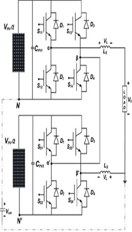
Fig. 1. PV-supported transformer less single-phase five-level cascaded multi-level inverter.
Between the modulation strategy and the leakage current. The cascaded H-bridge mu ltilevel inverter has the advantages of less leakage current as co mpared to the conventional single H-b ridge inverter due to reduced value of dc-lin k voltage per b ridge. The co mmon mu lticarrier modulation techniques used in the
transformer less cascaded H-bridge multilevel PV inverter topologies introduce common mode voltage.
This letter proposes a hybrid multicarrier pulse width modulation (H-M CPWM) technique to reduce leakage current in transformer less cascaded H-bridge mu ltilevel inverter for PV systems. When the common mode voltage changes in a large step value, it induces high leakage current in the PV system through the parasitic capacitance between the PV module and the ground. The reduced voltage transition in the co mmon mode voltage reduces the leakage current. It is easy to implement the proposed modulation technique without much complexity and require half the number of carriers as required in the conventional MCPWM techniques.
II. CASCADED MULTILEVEL INVERTER AND HYBRID MULTICARRIER MODULATION SCHEME FOR CONSTANT COMMON MODE
VOLTAGE
Fig. 1 shows the PV-supported single-phase five-level cascaded bridge inverter topology, where two H-bridges are connected in cascade and provides a common output. The configuration of two cascaded H-bridges adds the output voltage of the upper and lower bridges to generate five-level stepped output voltage at the ac side, i.e., VP V , VP V/2, 0, −VP V/2, and −VP V . It is assumed
that the grid does not contribute common mode voltage in the system [9]. The converter topology and modulation method have significant contribution in leakage current generation. Therefore, the transformer less cascaded mu ltilevel inverter shown in Fig. 1 is connected to a simp le resistive load for Evaluation of the proposed modulation technique. The leakage current is generated in the parasitic capacitance formed between the PV module and the ground, where common mode voltage is also induced at the same point as shown in Fig. 1. The common mode voltage of any electrical circu it is the mean value of voltage between the outputs and a common reference point.
The negative terminal of the dc bus, i.e., terminal N is called here as co mmon reference point fo r upper H-bridge inverter. Similarly, fo r lo wer H-bridge inverter, N_ is the
common reference point. The parasitic capacitance formed for the lo wer H-bridge and upper H-bridge is assumed to be the same, be-cause both the H-bridges are supplied fro m the similar rated PV modules [11]. The common mode voltage (CM V) and leakage current in the two H-bridges are also same; hence, the capaci-tive currents flow fro m point N to g round and N_ to ground is
considered equal. The co mmon mode voltage Vcm for the
Available online:
http://edupediapublications.org/journals/index.php/IJR/
P a g e | 759[3]:
Vcm=
Vα N +Vβ N
(1) 2
where Vα N and Vβ N are the voltages between the mid-point of the upper H-bridge inverter legs to the negative terminal o f the dc link, Vα_β_ is the voltage between the mid points of the two legs of the lower H-bridge inverter, and let Vo is the output voltage across the load. The leakage current mainly depends upon the magnitude of the inverter common mode voltage. In order to derive the expression of the common mode voltage in the cascaded mu ltilevel inverter, the fo llo wing equations can be written from Fig. 1:
Vcm+ Vα N − VL − VO = 0 (2)
Vcm+ Vβ N + VL − Vα _β _ = 0. (3)
The output voltage Vo has little effect on parasitic capacitance and hence it is neglected. It is assumed that the filter inductance Ls is considered the same in the two H-bridges for simp licity of the analysis and hence the voltage drop VL due to the inductance Ls in the two H-bridges is also assumed equal [3]. The expression of the common mode voltage can be obtained in (4) by adding (2) and (3) as follows:
2Vcm + Vβ N + Vα N −Vα_β_ = 0. (4)
Using (4), the common mode voltage can be expressed as follows:
Vcm =
Vα _β _ − Vα N − Vβ N
. (5)
2
Now considering convention that the leakage current will flow fro m PV module to ground or vice versa as per the standards IEEE 80 [22], the sign of co mmon mode voltage can be reversed as Vcm_ = −Vcm and abbreviated
now onward as CMV in this paper. Equation (5) is useful for determining the common mode voltage in various intervals of the reference period.
To minimize the leakage current flo w through the para-sitic capacitance, the co mmon mode voltage is required to be maintained minimu m during the switching instances. The minimu m step value of the common mode voltage is defined by VP V/(n − 1) in the M CPWM technique [18].
In phase
disposition mu lticarrier pulse width modulation (PD-MCPWM), the co mmon mode Vc m_ varies in the band
range of ±VP V /2. However, in this modulation method,
total (n−1) nu mber of carrier signals are used, where n is the inverter level. The proposed H-MCPWM is the modified version of the phase opposite disposition (POD) pulse width modulation technique, where the number of carriers required is half of that required in POD PWM and therefore computational burden is reduced. In this modulation method, the carrier signals used are in-phase with each other. The phase of all the carriers is shifted by 180° after each half-cycle. Tab le I shows the different switching in-stants and their corresponding magnitude of CM V. It has six switching instants, in which one instant has zero CM V, three in-stants have 2VP V /4, and two
instants have VP V/4, CM V. There is no voltage transition
in zero CM V. The CM V may take the values depending upon the inverter switch states selected since the voltage-source inverter cannot provide pure sinusoidal volt-ages and has discrete output voltage levels synthesized fro m the output voltage of the PV [10], [23]. The voltage transition depends upon the direction of the current in the inverter; hence, the proposed H-MCPWM modulation technique ensures the re-duced common mode voltage generation in the band limit of maximu m ±VP V /4. The
switching pattern of the proposed H-M CPWM technique for five-level cascaded multilevel inverter is illustrated in Fig. 2. The operation of the proposed H-MCPWM is divided into two modes of operation, i.e., mode-1 and mode-2, as explained next
A. Mode-1 (0 to T/2)
In this mode, all the carrier signals are in-phase with each other, the three-level voltages, i.e., 0, −VP V/2, and −VP V , are generated using following switching scheme:
Available online:
http://edupediapublications.org/journals/index.php/IJR/
P a g e | 760carrier signals Vc1 and Vc2 , then the switches S11 , S14 , S23 , and S22 are turned ON and the
complimentary switches, S13, S12, S21, and S24, are
turnedOFF. In this situation Vα N = VP V /2, Vβ N = 0,
and the output voltage is Vα β =+VP V/2.
2) When the reference signal Vref is greater the carrier
sig-nal Vc2 , and lesser than the carrier signal Vc1 ,
then the switches S14 , S12 , S23 , and S22 are turned
ON and the
complimentary switches S11 , S13 , S21 , and S24 are
turned OFF. In this situation Vα N = 0, Vβ N = 0, and the output voltage is Vα β = 0.
Fig. 2. Switching pattern of the proposed H-MCPWM technique for the fivelevel cascaded multilevel inverter.
3) When both the carrier signals, Vc 1 and Vc 2 , are
smaller than the reference signal Vref , then the
switches, S13 , S12, S23, and S22, are turnedONand
the complimentary
switches, S11 , S14 , S21 , and S24 , are turned OFF. In
this situation Vα N = 0, Vβ N=VP V/2, and the output
voltage is Vα β = −VP V/2.
In this mode, all the carrier signals are phase shifted by 180°, the three-level voltages, i.e., 0, +VP V/2, and +VP V ,
are generated using following switching scheme.
1) When the reference signal Vre f is s maller than the
carrier signals Vc1 and Vc2 , then the switches, S11 , S14 , S23 , and S22 , are turned ON and the
complimentary switches,
S13, S12, S21, and S24, are turnedOFF. In this
situation Vα _N _ = 0, Vβ _N _ = +VP V /2, and the
output voltage is
Vα _β _ = −VP V /2. When the reference signal Vref is
greater the carrier sig-nals Vc1 , and lesser than the
carrier signal Vc2 , then the switches, S11 , S14 , S21 ,
and S23 , are turned ON and the complimentary
switches, S13 , S12 , S22 , and S24, are turnedOFF. In
this situation Vα _N _ = +VP V /2, Vβ _N _ = +VP V /2,
and the output voltage is Vα _β _ = 0.
3) When both the carrier signals, Vc 1 and Vc 2 , are
smaller than the reference signal Vref , then the
switches, S11 , S14, S21, and S24, are turned ONand
the complimentaryswitches, S13 , S12 , S23 , and S22 ,
are turned OFF. In this situation Vα_N_ = VP V/2, Vβ_N_ = 0, and the output volt-
age is Vα_β_ = +VP V/2.
The summary of the switching instants employed in two modes of operation is presented in Table I. It is clearly visi-ble fro m the previous discussion that the proposed H-MCPWM technique is able to generate five-level inverter output voltage and attain reduced common mode voltage in the band of maxi-mu m ±VP V/4, which is
superior to the conventional MCPWM technique. III. INDUCTION MOTOR
Available online:
http://edupediapublications.org/journals/index.php/IJR/
P a g e | 761speed below base speed, then v/f ratio is to be kept constant so that flux remains constant. This retains the torque capability of the machine at the same value. But at lower frequencies, the torque capability decrease and this drop in torque has to be compensated for increasing the applied voltage. Any reduction in the supply frequency without a change in the terminal voltage causes an increase in the air gap flu x. Induction motors are designed to operate at the knee point of the magnetization characteristic to make full use of the magnetic material. Therefore the increase in flu x will saturate the motor. This will increase the magnetizing current, d istort the line current and voltage, increase the core loss and the stator copper loss, and produce a high pitch acoustic noise. While any increase in flu x beyond rated value is undesirable fro m the consideration of saturation effects, a decrease in flux is also avoided to retain the torque capability of the motor. Therefore, the variable frequency control below the rated frequency is generally carried out by reducing the machine phase voltage, V, along with the frequency in such a manner that the flu x is maintained constant. Above the rated frequency, the motor is operated at a constant voltage because of the limitation imposed by stator insulation or by supply voltage limitations.
IV MATLAB/SIMULATION RESULTS
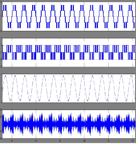
Fig 3 Matlab/simulation model of proposed converter with multi carrier modulation
Fig 4 Matlab/simulation wave form of proposed converter with in-phase deposition
Available online:
http://edupediapublications.org/journals/index.php/IJR/
P a g e | 762Fig 6 Matlab/simulation wave form of proposed converter with multi carrier deposition
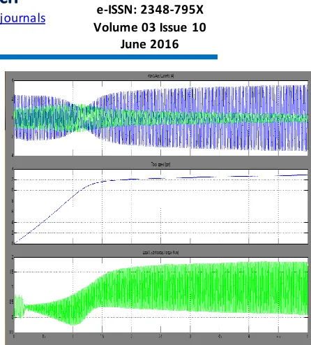
Fig 7 Matlab/simulation model of proposed converter with multi carrier modulation with Induction Motor drive
Fig.8 simulation waveforms of performance of induction motor
V CONCLUSION
In this project proposes H-MCPWM technique employed in transformer less cascaded multilevel inverter for the PV systems. The proposed modulation technique attains reduced common mode voltage with simplicity in implementation of the modulation technique. It has been illustrated that the proposed modulation technique has less leakage current as compared to the two-and three-level inverters. It is also observed that the proposed H-MCPWM offers less total harmonic distortion as compared to the conventional modulation methods. It uses only two carrier signals to generate the five-level inverter output which otherwise is four in other multicarrier modulation techniques , and to reduced ripple carrier current and also to study the Induction motor characteristics.
REFERENCES
[1] R. Gonzalez, J. Lopez, P. Sanchis, and L. Marroyo,
“Transformerless inverter for single-phase photovoltaic systems,”
IEEE Trans. Power Elec-tron., vol. 22, no. 2, pp. 693–697, Mar.
2007.
[2] Y. Wensong, L. Jih-Sheng, H. Qian, and C. Hutchens, “High -efficiency MOSFET inverter with H6-type configuration for photovoltaic nonisolated 1783
AC-module applications,” IEEE Trans. Power Electron., vol. 26, no. 4,1253–1260, Apr. 2011.
[3] Y. Zhou, W. Huang, P. Zhao, and J. Zhao, “A transformerless grid
-connected photovoltaic system based on the coupled inductor single-stage boost three-phase inverter,” IEEE Trans. Power Electron., vol. 29, no. 3,
pp. 1041–1046, Mar. 2014.
[4] L. Zhang, K. Sun, Y. Xing, and M. Xing, “H6 transformerless full
-bridge PV grid-tied inverters,” IEEE Trans. Power Electron., vol. 29, no. 3,
Available online:
http://edupediapublications.org/journals/index.php/IJR/
P a g e | 763[5] T. Kerekes, R. Teodorescu, P. Rodriguez, G. Vazquez, and E.
Aldabas, “A new high-efficiency single-phase transformerless PV
inverter topology,” IEEE Trans. Ind. Electron., vol. 58, no. 1, pp.
184–191, Jan. 2011.
[6] E. Koutroulis and F. Blaabjerg, “Design optimization of
transformerless grid-connected PV inverters including reliability,”
IEEE Trans. PowerElectron., vol. 28, no. 1, pp. 325–335, Jan. 2013.
[7] L. June-Seok and L. Kyo-Beum, “New modulation techniques for
a leak-age current reduction and a neutral-point voltage balance in transformer-less photovoltaic systems using a three-level inverter,”
IEEE Trans. PowerElectron., vol. 29, no. 4, pp. 1720–1732, Apr. 2014.
[8] Z. Li, S. Kai Sun, F. Lanlan, W. Hongfei, and X. Yan, “A family
of neutral point clamped full-bridge topologies for transformerless photovoltaic grid-tied inverters,” IEEE Trans. Power Electron., vol. 28, no. 2, pp. 730–739, Feb. 2013.
[9] Y. Bo, L. Wuhua, G. Yunjie, C. Wenfeng, and H. Xiangning,
“Improved transformerless inverter with common-mode leakage
current elimination for a photovoltaic grid-connected power
system,” IEEE Trans. PowerElectron., vol. 27, no. 2, pp. 752–
762, Feb. 2012.
[10] M. M. Renge and H. M. Suryawanshi, “Five-level diode clamped inverter to eliminate common mode voltage and reduce dv/dt in
medium voltage rating induction motor drives,” IEEE Trans.
Power Electron., vol. 23, no. 4, pp. 1598–1607, Jul. 2008.
[11] Y. Zhou and H. Li, “Analysis and suppression of leakage current in cascaded-multilevel-inverter based PV systems,” IEEE Trans.
Power Elec-tron., vol. 29, no. 10, pp. 5265–5277, Oct. 2014.
[12] R. Gonzalez, E. Gubia, J. Lopez, and L. Marroyo,
“Transformerless single phase multilevel-based photovoltaic
inverter,” IEEE Trans. Ind. Electron., vol. 55, no. 7, pp. 2694–
2702, Jul. 2008.
[13] (2014). [Online]. Available: http://www.sungrowpower.com
[14] S. Gautam and R. Gupta, “Switching frequency derivation for the
cas-caded multilevel inverter operating in current control mode using multi-band hysteresis modulation,” IEEE Trans. Power Electron., vol. 29, no. 3,
pp. 1480–1489, Mar. 2014.
[15] A. M. Hava and E. Un, “A high-performance PWM algorithm for common-mode voltage reduction in three-phase voltage source invert-ers,” IEEE Trans. Power Electron., vol. 26, no. 7, pp. 1998–
2008, Jul. 2011.
[16] K. Zhou and D. Wang, “Relationship between space-vector modulation and three-phase carrier-based PWM: A comprehensive
analysis,” IEEETrans. Ind. Electron., vol. 49, no. 1, pp. 186–196,
Jan. 2002.
[17] L. P. Chiang, D. G. Holmes, Y. Fukuta, and T. A. Lipo, “Reduced
common-mode modulation strategies for cascaded multilevel
inverters,” IEEE Trans. Ind. Appl., vol. 39, no. 5, pp. 1386–1395,
Sep./Oct. 2003.
[18] L. Poh Chiang, D. G. Holmes, and T. A Lipo, “Implementation
and control of distributed PWM cascaded multilevel inverters with minimal harmonic distortion and common-mode voltage,” IEEE Trans. Power Electron., vol. 20, no. 1, pp. 90–99, Jan. 2005.
[19] C. C Hou, C. C. Shih, P. T. Cheng, and A. M. Hava, “Common -mode voltage reduction pulsewidth modulation techniques for three-phase grid-connected converters,” IEEE Trans. Power Electron., vol. 28, no. 4,
pp. 1971–1979, Apr. 2013.
[20] G. Xiaoqiang, M. C. Cavalcanti, A. M. Farias, and J. M. Guerrero,
“Single-carrier modulation for neutral-point-clamped inverters in
three-phase transformerless photovoltaic systems,” IEEE Trans.
Power Elec-tron., vol. 28, no. 6, pp. 2635–2637, Jun. 2013.
[21] O. Lopez, R. T eodorescu, and J. Doval-Gandoy, “Multilevel
transformer-less topologies for single-phase grid-connected
converters,” in Proc. 32ndAnnu. Conf. IEEE Ind. Electron., Nov.
2006, pp. 5191–5196.
[22] IEEE Guide for Safety in AC Substation Grounding, IEEE Std. 80-2000,New York, NY, USA, 2000.
[23] R. M. Mohan and S. M. Hiralal, “Multilevel inverter to reduce
common mode voltage in AC motor drives using SPWM
technique” J. PowerElectron., vol. 11, no. 1, pp. 21–27, Jan. 2011.
[24] D. G. Holmes and T. Lipo, Pulse Width Modulation for Power
Converters:Principles and Practice. Piscataway, NJ, USA: IEEE
Available online:
http://edupediapublications.org/journals/index.php/IJR/
P a g e | 764Authors profile:
JAREENA M.Tech student Scholar Presently pursuing M.Tech in prestigious Sri Indu Institute of Engineering & Technology, Hyderabad,India
K. Murali is presently working as Assistant professor in prestigious Sri Indu Institute of Engineering & Technology, Hyderabad, India.