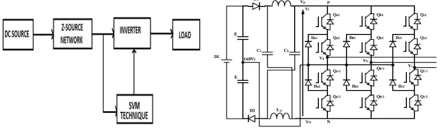
Copyright to IJIRSET www.ijirset.com 209
Design and Implementation of space Vector Modulated
Three Level Inverter with Quasi-Z-Source Network
Ranjutha.G1, Kumaresan.R2
PG Student [PED], Dept. of EEE, KSR College of Engineering, Thiruchengode, Tamilnadu, India 1 Assistant professor, Dept. of EEE, KSR College of Engineering, Thiruchengode, Tamilnadu, India 2
ABSTRACT: A three level inverters with single quasi z-source neutral point clamped inverter using the space vector modulation technique is proposed in this paper. The proposed inverter has the main features in that the output voltage can be bucked or boosted and in-phase with the input voltage. The quasi z-source concept can be applied to all DC-AC, AC-DC and AC-DC-AC-DC power conversion whether two-level or multi-level. Previous publications have shown the control of a Z-source neutral point clamped inverter using the space vector modulation technique. A three level inverters with single quasi Z-source is proposed in this project. This gives a number of benefits, both in terms of implementation and harmonic performance. The experiment results verified that the inverter has the lower input current harmonics distortion, a high efficiency, as it makes possible to avoid voltage spikes on the switches.
KEYWORDS: Buck–boost, neutral point clamped inverter, space vector modulation (SVM), quasi Z-source inverter.
I.
I
NTRODUCTIONdevelopment of a modified SVM algorithm for controlling the REC Z-source NPC inverter. The theoretical development is discussed in detail, and simulations as well as experimental results are used to verify the operation of the circuit and proposed SVM-based modulation.
Fig. 1. Schematic of Z-Source inverter Fig. 2. Circuit of an REC Z source NPC inverter.
II. REVIEW OF QUASI Z-SOURCE CONCEPT
Fig. 3. Structure of the proposed quasi Z source inverter. Fig. 4. Circuit of an quasi Z source NPC inverter
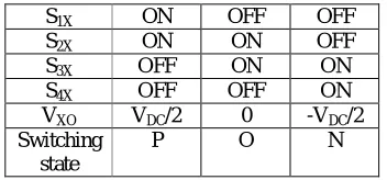
III. TOPOLOGY OF QUASI Z-SOURCE NPC INVERTER
To describe the operating principle of the quasi Z-source NPC inverter shown in Fig. 4, we concentrate initially on the operation of one phase leg. The operation of each inverter phase leg of a traditional NPC inverter can be represented by three switching states P, O, and N. Switching state “P” denotes that the upper two switches in a phase leg are gated ON, “N” indicates that the lower two switches conduct, and “O” signifies that the inner two switches are gated ON.
Copyright to IJIRSET www.ijirset.com 211
Fig. 5. Equivalent circuit of qZSI in active mode Fig. 6. Equivalent circuit of qZSI in shoot through mode IV. OPERATING MODES OF QZSI In the non-shoot through mode, the switching pattern for the qZSI is similar to that of a VSI. The inverter bridge, viewed from the DC side is equivalent to a current source the input DC voltage is available at the DC link voltage input to the inverter, which makes the qZSI behave similar to a VSI.In the shoot through mode, switches of the same phase in the inverter bridge are switched on simultaneously for a very short duration. The source however does not get short circuited when attempted to do so because of the presence LC network, while boosting the output voltage. The DC link voltage during the shoot through states, is boosted by a boost factor, whose value depends on the shoot through duty ratio for a given modulation indexSimilar to the existing qZSI operating principle [11], the system in Fig. 4 also has two operating modes in the continuous conduction mode (CCM). 1) Mode I:This mode will make the inverter short circuit via any one phase leg, combinations of any two phase legs, and all three phase legs in Fig. 4, which is referred to as the shoot through state [11]. As a result, the diode Dz is turned off due to the reverse-bias voltage. Its equivalent circuit is shown in Fig. 6. During this time interval, the circuit equations are presented as follows C = iB –iL2 (1)
C = -iL1 (2)
L = Vin + VC2 (3)
L = VC1 (4)
where iL1, iL2, and iB denote the currents of inductors L1 and L2 and the battery, respectively; VC1, VC2, and Vin denote the voltages of capacitors C1 and C2 and the PV panel, respectively; C denotes the capacitance of capacitors C1 and C2; and L denotes the inductance of inductors L1 and L2. 2) Mode II: This mode will make the inverter operate in one of the six active states and two traditional zero states, which is referred to as the non-shoot-through state [11]. A continuous current flows through the diode Dz, and its equivalent circuit is shown in Fig. 6. During this time interval, the circuit equations are presented as follows: C = iB +iL1-id (5)
C = iL2 - id (6)
L = Vin - VC1 (7)
L = -VC2 (8)
where id is the load current going to the inverter.
A. Inverter System Model
We define T0 as the time interval for Mode I and T1 as the time interval for Mode II, with a switching cycle T. The shoot-through duty ratio is then defined as D = T0/T , and
T = T0 + T1.
TABLE 1
Comparison of Current Behavior for Two Inductors Input and Output
Power Relationship
Battery Power
Inductor Currents
Pin<Pout PB>0 iL2 < iL1 iL2 > iL1
Pin<Pout PB<0 iL2 > iL1 iL2 < iL1
Pin=Pout PB=0 iL2 = iL1 iL2 = iL1
B. Analysis and Comparison According to (1) and (13), in Fig. 2, the following can be observed. 1) If Pin < Pout, PB > 0, and iL2 > iL1, the battery is discharging. 2) If Pin > Pout, PB < 0, and iL2 < iL1, the battery is charging.
3) If Pin = Pout, PB = 0, and iL2 = iL1, the battery will not have energy exchange.
Fig. 1 shows significantly different performances because the average currents of its two inductors and battery have the following expression:
iL2 − iL1 = −iB. (9)
Table I summarizes both circuits’ current behaviors, which presents inverse current relationships for the two inductors when the battery charges and discharges. In addition, the new topology in Fig. 2 works in the CCM, if
iD = iL2 + iC1 − iB > 0 (10) during Mode II; otherwise, it works in the DCM if iD = 0 during Mode II.
In steady state, the average current of capacitor C1 is zero, and (10) will become
iB < iL2 or iL1 > 0. (11)
The power equation should satisfy the following inequality:
PB < Pout. (12)
Table 2
Switching combination and switching states for a three level inverter (1 phase leg)
S1X ON OFF OFF
S2X ON ON OFF
S3X OFF ON ON
S4X OFF OFF ON
VXO VDC/2 0 -VDC/2
Switching state
Copyright to IJIRSET www.ijirset.com 213
Among the three-level quasi Z-source power converter topologies reported to date, the quasi Z-source NPC inverter implemented using a single LC impedance network (see Fig. 4) is considered to be an optimized topology in terms of component count [12], [13]. Referring to Fig. 4, the quasi Z-source NPC inverter is supplied with a split dc source. The middle point O is taken as a reference. By controlling the switches of each phase leg according to the combinations presented in Table I, each output phase voltage Vxo (x_{a, b, c}) has three possibilities: Vi/2, 0, and −Vi/2. When the quasi Z-source NPC inverter is operated without any shoot-through states, then Vi is equivalent to 2E. As noted earlier, with this kind of operation, the maximum obtainable output line-to-line voltage cannot exceed the available dc source voltage (2E). Therefore, to obtain an output line-to-line voltage greater than 2E, shoot-through states are carefully inserted into selected phase legs to boost the input voltage to Vi > 2E before it is inverted by the NPC circuitry. Thus, the REC Z-source inverter can boost and buck the output line-to-line voltage with a single-stage structure. In [5], two new switching states namely the UST and LST states were identified, in addition to the FST state and the non shoot-through (NST) states (P, O, and N) that had been reported earlier in [10]. Although operation using the FST and NST states possible (termed the FST operating mode), it is generally preferable to use the UST and LST states in place of the FST states (termed the ULST operating mode). The ULST operating mode is preferred because it produces an output voltage with enhanced waveform quality. The simplest FST operating mode requires all four switches in a phase leg (see Table I) to be turned ON. This is not aminimal loss approach since, for example, switching phase A from +E through FST to 0 V would require switches {Sa1, Sa2, Sa’1,Sa’2} changing from {ON, ON, OFF, OFF} through {ON,ON, ON, ON} to {OFF, ON, ON, OFF}. An alternative FST operating mode which gives minimal loss uses two phase legs to create the shoot-through path. This requires, for example, synchronization of the turn ON instants of switches Sa1 from phase A and Sc’2 from phase C at the start of an FST state. Doing so creates a time interval during which switches {Qa1, Qa2, Qa’1} from phase A and {Sc2, Sc’1, Sc’2} from phase C are gated ON simultaneously to create a shoot-through path [35].
However, the output line-to-line voltage obtained using the minimal loss FST approach has higher harmonic distortion (compared to the ULST approach) in its output voltage waveform because the voltage levels produced do not have adjacent level switching [35]. Therefore, in this paper, the ULST operating mode is used for controlling the quasi Z-source NPC inverter. Assuming that the Z-source network is symmetrical (L1 = L2 = L and C1 = C2 = C), then VL1 = VL2 = VL and VC1 = VC2 = VC and the voltage expressions for the NST state are as follows:
NST
VL = 2E − VC (13)
VP = +Vi/2, VN = −Vi/2 (14)
VI = 2(VC − E) (15)
Similarly, the voltage expressions for the UST and LST states are as follows:
UST
VL1 = E (16)
VP = 0 V, VN = E − VC1 (17)
LST
VL2 = E (18)
VP = −E + VC2, VN = 0 V (19) We denote the duration of the NST, UST, and LST states by TN, TU, and TL, respectively, and the switching period by T.
Also, we assume that TU and TL are equal (this is necessary to ensure symmetrical operation) and denote the total combined UST and LST duration by TULST. At steady state, the average voltage across the inductors is zero; therefore, averaging the inductor voltage over one switching period, we have
TN + TU + TL = T (21)
Solving for VC using (20) and (21), we have
VC = 2E . {
⁄
} (22)
Substituting (22) into (15), we have the dc-link voltage Vi during the NST state as
Vi-NST = { } (23)
Similarly, when (22) is substituted into (17) and (19) and noting that Vi = VP − VN , we have the dc-link voltage during the UST and LST states as
Vi-UST = Vi – LST = { } (24)
It is noted from (23) and (24) that the higher dc-link voltage is present during the NST states and it is twice the dc-link voltage available during the UST and LST states, as required.
The fundamental peak ac output voltage Vxo (xE{a, b, c}) is given by
VX0 =
⎷ . Vi-NST (25) VX0 = ( ) {
⎷ (2E)} = B’{⎷ (2E)} (26)
Where B≥ 1 is the boost factor and all the other symbols have their usual meaning.
Fig. 7. Space vector diagram of a three-level inverter
V. MODIFIED SVM OF THE REC QUASI Z-SOURCE NPC INVERTER
A. Duty Cycle Calculation
The space vector diagram of a traditional NPC inverter for sector 1 is shown in Fig. 4. The reference vector
V
refcan beCopyright to IJIRSET www.ijirset.com 215
Vref(t) = [va0(t)ej0 + Vb0(t)e π + VC0(t)e π (27)
d1. ͞v1 + d2. ͞v7 + d3.͞v13= ͞vref (28)
d1 + d2 + d3 = 1 (29)
͞v1 = . (2E) (30)
͞v7 = ⎷ . e . (2E) (31)
͞v13 = . (2E) (32)
͞vref = V ref . e jƟ (33)
Substituting (19) into (18), the duty ratios of the nearest three voltage vectors are given by (20), where M is the modulation index and 0 ≤ θ ≤ π/3 d1 = 2 – 2M sin ( + Ɵ) d2 = 2 – 2M sin Ɵ d3 = 2M sin ( – Ɵ) (34)
A similar procedure is used for calculating the duty ratios of the selected voltage vectors in all the other triangles. To complete the modulation process, the selected voltage vectors are applied to the output according to a switching sequence. Ideally, a switching sequence is formed in such a way that a high quality output waveform is obtained with minimum number of switching transitions.
VI. SIMULATION RESULTS
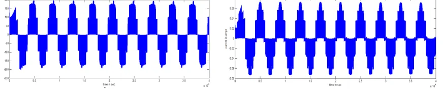
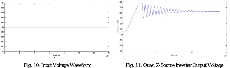
The simulation for the space vector modulated three level inverter with Quasi z-source inverter has been done by using the MATLAB/SIMULINK. The conventional Z-source inverter output waveform is shown in Fig. 8.. The input voltage is 150V. The space vector modulated three level inverter with a single Z-source inverter boosted the 170V of the output waveform. It has high total harmonic distortion. The input voltage of the inverter is Fig. 10, Constant 150V is given to the Quasi Z source inverter. The Quasi Z Source inverter is boost the input voltage. qZSI output voltage is shown in Fig. 11.
Fig. 10. Input Voltage Waveform Fig. 11. Quasi Z-Source Inverter Output Voltage
The Quasi Z-source inverter output waveform is shown in Fig. 12. The input voltage is 150V. The space vector modulated three level inverter with Quasi Z-source inverter boosted the 210V of the output waveform. It improves the current and voltage gain. The qZSI current waveform is shown in Fig. 13.
Fig. 12. Quasi Z source inverter output voltage waveform Fig. 13. Quasi Z source inverter output current waveform
Fig.14. THD waveform
Fig. 14, shows the harmonics present in the output THD value is 5.10%. The harmonic reduction is achieved by selecting the appropriate switching angles. The space vector modulated three level inverter with Quasi Z-source inverter reduces the total harmonic distortion.
VI. CONCLUSION
second average and voltage boosting capability regardless of the angular position of the reference vector. The insertion of the shoot- through states was such that the number of device commutations was kept at a minimum of six per sampling period, similar to that needed by a traditional NPC inverter. The presented concepts have been verified in simulations and validated experimentally using a three-phase quasi Z-source NPC inverter prototype.
REFERENCES
[1] S.Busquets-Monge, J. Rocabert, P. Rodriguez, S. Alepuz, and J.Bordonau, “Multilevel diode-clamped converter for photovoltaic generators with independent voltage control of each solar array,” IEEE Trans.Ind. Electron., vol. 55, no. 7, pp. 2713–2723, Jul. 2008.
[2] Z. Zhao, Y. Zhong, H. Gao, L. Yuan, and T. Lu, “Hybrid selective harmonic elimination PWM for common-mode voltage reduction in three level neutral-point-clamped inverters for variable speed induction drives,” IEEE Trans. Power Electron., vol. 27, no. 3, pp. 1152–1158, Mar. 2012.
[3] S. Dehghan, E. Seifi, M. Mohamadian, and R. Gharehkhani, “Grid connected DG systems based on Z-source NPC inverters,” in Proc. 2nd Power Electron. Drive Syst. Technol. Conf., Feb. 2011, pp. 104–110.
[4] X. Fang, M. Cao, and Z. Chen, “Z-sourceAC-DC-AC converter for mining applications,” in Proc. Int. Conf. Electr.Mach. Syst., Oct. 2010, pp. 44–47. [5] P. C. Loh, F. Gao, F. Blaabjerg, and S. W. Lim, “Operational analysis and modulation control of three-level Z-source inverters with enhanced output waveform quality,” IEEE Trans. Power Electron., vol. 24, no. 7, pp. 1767–1775, Jul. 2009.
[6] J. Pou, J. Zaragoza, S. Ceballos, M. Saeedifard, and D. Boroyevich, “A carrier-based PWM strategy with zero-sequence voltage injection for a three-level neutral-point-clamped converter,” IEEE Trans. Power Electron.,vol. 27, no. 2, pp. 642–651, Feb. 2012.
[7] J. Boys and P. Handley, “Harmonic analysis of space vector modulated PWM waveforms,” IEE Proc.—Electr. Power Appl., vol. 137, no. 4, pp. 197– 204, Jul. 1990.
[8] D. Holmes, “The general relationship between regular-sampled pulsewidth- modulation and space vector modulation for hard switched converters,” in Proc. Conf. Rec. IEEE Ind. Appl. Soc. Annu. Meet., Oct. 1992, vol. 1, pp. 1002–1009.
[9] H. van der Broeck, H.-C. Skudelny, and G. Stanke, “Analysis and realization of a pulsewidth modulator based on voltage space vectors,” IEEETrans. Ind. Appl., vol. 24, no. 1, pp. 142–150, Jan./Feb. 1988.
[10] P. C. Loh, S. W. Lim, F. Gao, and F. Blaabjerg, “Three-level Z-source inverters using a single LC impedance network,” IEEE Trans. Power Electron., vol. 22, no. 2, pp. 706–711, Mar. 2007.
[11] J. Anderson and F. Z. Peng, “A class of quasi-Z-source inverters,” in Conf. Rec. IEEE IAS Annu. Meeting, Edmonton, AL, Canada, Oct. 2008, pp. 1– 7.
[12]P. C. Loh, F. Gao, and F. Blaabjerg, “Embedded EZ-source inverters,” IEEE Trans. Ind. Appl., vol. 46, no. 1, pp. 256–267, Jan./Feb. 2010. [13] F. Gao, P. C. Loh, F. Blaabjerg, R. Teodorescu, and D. Vilathgamuwa, “Five-level Z-source diode-clamped inverter,” Power Electron. IET, vol. 3, no. 4, pp. 500–510, Jul. 2010.
[14] F. Z. Peng, “Z-source inverter,” in Proc. Conf. Rec. 37th IAS Annu. Meet. Ind. Appl. Conf., Oct. 2002, vol. 2, pp. 775–781.