Compact Microstrip BPF with High Selectivity Using Extended
Tapped Lines
Yi-Qiang Gao1, 2, Wei Shen3, Liang Wu1, and Xiao-Wei Sun1, *
Abstract—This paper proposes a compact microstrip bandpass filter (BPF) with high selectivity. A folded stepped-impedance resonator (SIR) of which the high impedance part is realized by a coplanar waveguide on the ground layer is introduced to the filter design for miniaturization. Furthermore, source-load coupling is implemented by extended tapped lines (ETLs). High selectivity with four transmission zeros (TZs) can be achieved. The analysis of the filter is presented based on a transmission line circuit model and even- and odd-mode analysis method. An experimental filter with the size of 0.15λg∗0.13λg
(where λg is the guide wave-length at the center frequency) is designed to validate our methods.
1. INTRODUCTION
With the increasing tension of spectrum resources, highly selective filters have become an important part of the front-ends. Bandpass filters (BPFs) can be an effective choice to obtain the required signal to noise ratio. Various techniques have been introduced to achieve transmission zeros (TZs) to realize high selectivity. Cross-coupling and source-load coupling are used simultaneously in a fourth-order waveguide BPF to achieve four near band TZs [1]. Stepped-impedance resonators with mixed cross-coupling are proposed to achieve one more TZ [2]. In addition, source-load coupling is also an easy way to accomplish better selectivity. A large number of studies have used sourceload coupling to achieve transmission zeros (TZs) near the passband and realize high selectivity [3–9]. Four shorted quarter-wavelength coplanar waveguide (CPW) resonators as well as shorted CPW excitation lines are introduced to realize capacitive crosscoupling and inductive source-load coupling respectively [3]. The filter with better frequency skirt is achieved with six TZs. However, the implementation is complicated as bonding wires are needed to keep common ground. A dual mode resonator with capacitive and inductive source-load coupling is analyzed in [4, 5], respectively. But only one TZ can be placed really near the passband. A simple and effective second-order BPF with a TZ on each side of the passband is realized by parallel coupled quarter-wavelength resonators and inductive source-load coupling [6]. Mixed source-load coupling is adopted in the substrate integrated waveguide (SIW) [7, 8] and microstrip filters [9]; three TZs can be obtained. In general, however, the dimensions of SIW filters can be larger than the microstrip ones in low frequency.
In this paper, a compact BPF with high selectivity is designed using a novel source-load coupling structure. Extended tapped lines (ETLs) implemented at the I/O ports are used to excite the resonators as well as realize source-load coupling. Three TZs near the passband are obtained to improve frequency selectivity, and one TZ at high stopband is used to suppress a harmonic passband. Besides, a folded SIR is used to achieve miniaturization, of which the high impedance section is realized by CPW on the ground plane. In addition, transmission line circuit model as well as odd- and even-mode theory
Received 13 August 2018, Accepted 13 October 2018, Scheduled 20 November 2018
* Corresponding author: Xiao-Wei Sun ([email protected]).
1 Key Laboratory of Terahertz Solid-State Technology, Shanghai Institute of Microsystem and Information Technology, Shanghai
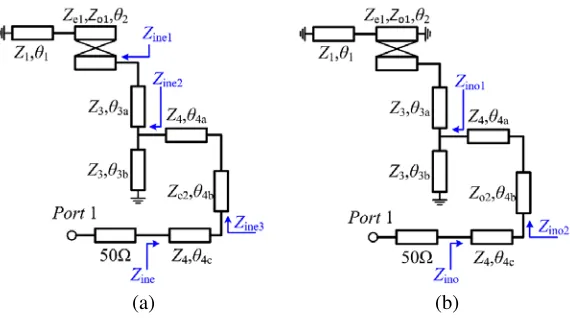
As shown in Fig. 1(a), the proposed filter consists of three parallel coupled shorted quarter-wavelength SIRs (Z1, Z2b) (Z3, Z2a). To achieve a larger coupling coefficient, three SIRs are arranged in the
interdigital form. ETLs (Z4) are used to excite resonator 1 (R1) and resonator 3 (R3), also a part of
the ETLs are coupled (Ze2, Zo2) to realize source-load coupling conveniently. According to [10], the three parallel coupled lines in dashed line frame can be transformed to two pairs of coupled lines (Ze1,
Zo1) with the center SIR separated to middle connected two SIRs illustrated in dashed line frame of Fig. 1(b).
(b) (a)
Figure 1. (a) Ideal transmission line circuit and (b) equivalent transmission line circuit of the proposed BPF.
Figure 2. The calculated results of the equivalent transmission line circuit shown in Fig. 1(b) (Z1 = 90 Ω, Zo1 = 32 Ω, Ze1 = 49 Ω, Z3 = 94 Ω, Z4 = 115 Ω, Zo2 = 79 Ω, Ze2 = 144.5 Ω, θ1 = 37.6 deg, θ2= 30 deg, θ3a= 5 deg, θ3b = 37.3 deg,θ4a= 5 deg,θ4b = 16 deg, θ4c = 42 deg).
The calculated results of the circuits in Fig. 1 are plotted in Fig. 2. The electric lengths of the transmission lines of Fig. 2 are calculated at the center frequency f0 = 2.4 GHz. Four TZs can be
(b) (a)
Figure 3. (a) Even-mode equivalent circuit. (b) Odd-mode equivalent circuit.
property of the circuit, the frequency responses can be derived by the odd- and even-mode analysis method [11]. The reflection response S11and transmission responseS21 are:
S11 =
(Y2
0 −YineYino)
(Y0+Yine)(Y0+Yino)
(1)
S21 = Y0
(Yino−Yine)
(Y0+Yino)(Y0+Yine)
(2)
The even- and odd-mode circuits are illustrated in Figs. 3(a) and 3(b), respectively. The input impedanceZino1 is
Zino1 = j(2T Z3tanθ3bcotθ2−Z
2
3tanθ3atanθ3b)
2T(1−tanθ3atanθ3b) cotθ2−Z3(tanθ3a+ tanθ3b)
(3a)
where
T = Ze1Zo1
Ze1+Zo1 (3b)
and input impedanceZino2 is
Zino2 = Zo2[Zino1(Z4−Zo2tanθ4atanθ4b) +jZ4(Z4tanθ4a+Zo2tanθ4b)]
Z4(Zo2−Z4tanθ4a) tanθ4b+jZino1(Z4tanθ4b+ tanθ4a)
(4)
Based on Equations (3)–(4) the input admittance of the odd-mode (Yino) can be derived as
Yino = Z4+jZino2tanθ4c Z4Zino2+jZ42tanθ4c
(5)
For the even-mode circuit in Fig. 3(b), the input impedance is
Zine1 = AC(j2Z1tanθ1) +B
(j2Z1tanθ1) +A
(6)
where
A = (Ze1+Zo1)/[(Ze1−Zo1) cosθ1] (7a)
B = j(Ze1−Zo1)
2−(Z
e1+Zo1)2cos2θ1
2(Ze1−Zo1) sinθ1
(7b)
C = 2 sinθ1/(Ze1−Zo1) (7c)
The input impedance Zine2 and Zine3 are
Zine2 = −Z
2
3tanθ3atanθ3b+jZ3Zine1tanθ3b Zine1(1−tanθ3atanθ3b) +jZ3(tanθ3a+ tanθ3b)
Yine= Z4+jZine3tanθ4c Z4Zine3+jZ42tanθ4c
(10)
Based on Equations (1)–(10), the functions of S-parameters depend on characteristic impedances, and electric lengths can be obtained easily.
2.1. Bandwidth and Port Excitation
The bandwidth of the proposed BPF is controlled by degree of the coupling among three parallel coupled SIRs. The bandwidths of the proposed BPF with differentZe1,Zo1 andK1 [K1= (Ze1Zo1)/(Ze1+Zo1)]
are plotted in Fig. 4(a). For a largerK1, the bandwidth of proposed BPF increases correspondingly. The
(b) (a)
Figure 4. (a) Bandwidths of the proposed BPF with differentZe1,Zo1andK1[K1= (Ze1−Zo1)/(Ze1+ Zo1)] (Z1 = 90 Ω, Z3 = 94 Ω, Z4 = 115 Ω, Zo2 = 79 Ω, Ze2 = 144.5 Ω, θ1 = 37.6 deg, θ2 = 30 deg, θ3a = 5 deg, θ3b = 37.3 deg, θ4a = 5 deg, θ4b = 16 deg, θ4c = 42 deg) (b) frequency responses of
the proposed BPF with different proportion of θ3a in θ3 (θ3 = θ3a +θ3b) (Z1 = 90 Ω, Zo1 = 32 Ω, Ze1 = 49 Ω, Z3 = 94 Ω,Z4= 115 Ω, Zo2 = 79 Ω,Ze2 = 144.5 Ω, θ1= 37.6 deg,θ2 = 30 deg, θ4a= 5 deg, θ4b = 16 deg, θ4c= 42 deg).
(b) (a)
Figure 5. Simulation results of (a) the extracted external quality factorQeagainstLt1(b) the extracted
degree of the port excitation can be easily tuned by adjusting the proportion ofθ3ainθ3(θ3 =θ3a+θ3b).
Calculated results are demonstrated in Fig. 4(b).
To further investigate the influences of physical dimensions on the port excitation and bandwidth, the extracted external quality factor Qe and the coupling coefficient k are simulated based on the
structures in Fig. 5(a) and Fig. 5(b), respectively. As demonstrated in Fig. 5, the quality factor Qe is
controlled by Lt1 while the coupling coefficient kis determined by s1.
2.2. Transmission Zeros
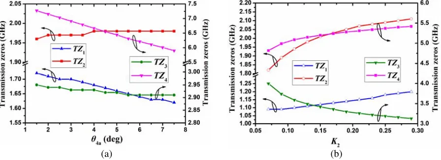
The TZs can be achieved by solving S21 = 0. Four TZs can be observed with two TZs located at the
lower stopband, and the other two TZs located at the upper stopband. The location of the TZs is mainly controlled by the ETLs. The effects of θ4a and K2 [K2 = (Ze2Zo2)/(Ze2 +Zo2)] on TZs are shown in
Fig. 6(a) and Fig. 6(b), respectively. As can be seen from Fig. 6(a),TZ1,TZ3 and TZ4 move to lower
frequencies, whileTZ2 moves to higher frequencies whenθ4aincreases. However, compared toTZ1 and
TZ4, the changes of TZ2 and TZ3 are very small compared with their frequencies As demonstrated in
Fig. 6(b), the locations of the TZs all change with K2 distinctly TZ1, TZ2 and TZ4 move to higher
frequencies, whileTZ3 moves to lower frequencies when K2 increases.
(b) (a)
Figure 6. (a) Transmission zeros versus θ4a (Z1 = 90 Ω, Zo1 = 32.3 Ω, Ze1 = 49.1 Ω, Z3 = 94 Ω, Z4 = 115 Ω, Zo2 = 79 Ω, Ze2 = 144.5 Ω, θ1 = 37 deg, θ2 = 30 deg, θ3a = 5 deg, θ3b = 37.3 deg, θ4b= 16 deg, θ4c = 42 deg) (b) transmission zeros versusK2 [K2= (Ze2−Zo2)/(Ze2+Zo2)] (Z1 = 90 Ω, Zo1 = 32.3 Ω, Ze1 = 49.1 Ω, Z3 = 94 Ω, Z4 = 115 Ω, Zo2 = 40 Ω, θ1 = 37 deg, θ2 = 30 deg, θ3a= 5 deg, θ3b= 37.3 deg, θ4b= 16 deg, θ4c= 42 deg).
In fact, the generation mechanisms of the TZs are different. Looking at the part in the green dotted frame in Fig. 1(b), the ETLs along with the shorted stub (Z3,θ3b) not only provide the
source-load coupling, but also produce two extra TZs. The frequency responses of differentθ4a are plotted in Fig. 7(a). The changing trends of the two TZs in Fig. 7(a) are same to those of TZ1 and TZ4, when θ4aincreases.
Above all, although the location of the TZs cannot be controlled individually, we can still arrange the distribution of the TZs by adjustingθ4a and K2. In addition, the extended part of the feeding line θ4a is implemented to suppress the harmonic band of the proposed BPF. The calculated results are
displayed in Fig. 7(b).
3. FULL WAVE SIMULATION AND MEASUREMENT
(b) (a)
Figure 7. (a) The frequency responses of the ETLs with different θ4a (Z1 = 90 Ω, Zo1 = 32.3 Ω, Ze1 = 49.1 Ω, Z3 = 94 Ω, Z4 = 115 Ω,Zo2 = 79 Ω,Ze2 = 144.5 Ω, θ1 = 37 deg,θ2 = 30 deg,θ3a= 5 deg, θ3b = 37.3 deg, θ4b = 16 deg, θ4c = 42 deg) (b) the calculated frequency responses of different θ4c
(Z1 = 90 Ω,Zo1 = 32.3 Ω, Ze1= 49.1 Ω, Z3 = 94 Ω,Z4 = 115 Ω,Zo2 = 79 Ω,Ze2= 144.5 Ω,θ1 = 37 deg, θ2 = 30 deg, θ3a= 5 deg, θ3b= 37.3 deg, θ4a= 5 deg, θ4b= 16 deg).
(b) (a)
Figure 8. (a) Physical configuration. (b) Design process of the center SIR.
layer and a high Z CPW section on the ground plane connected by a metalized via with the radius of 0.15 mm. It is transformed from the traditional microstrip SIR by replacing the high impedance microstrip section with a CPW one and rotating the CPW section to the bottom of the microstrip one. The design process is shown in Fig. 8(b). The input admittance Ys should be equal to zero under the
resonant condition. Thus,
Ys = Z 2
s2−Zs1Zs2tanθs1tanθs2
jZs2(Zs1tanθs1+Zs2tanθs2) = 0 (11a)
Zs2/Zs1 = tanθs1tanθs2 (11b)
(b) (a)
Figure 9. (a) Simulated and measured results of the proposed filter, (b) the pictures of the proposed BPF.
on Rogers RT/duroid 5880 (εr = 2.2, tanδ = 0.0009) with thickness of 0.508 mm is simulated and
measured. The specific dimension parameters are as follows: W1 = 2, W2= 0.5, W3 = 3.14, W4= 1.2, W5 = 0.5, W6 = 0.3,L1 = 8, L2 = 9.5, L3 = 9.0, L4 = 2.9,L5 = 12.56, Lu = 0.3,Lt= 1.1, s1 = 0.25, s2= 0.24, units in mm.
The simulated and measured results are plotted in Fig. 9 for comparison. The measured passband is centered at 2.4 GHz with FBW of 8.3%. The measured minimum insertion is 1.12 dB, with return loss better than 20 dB. Four TZs are located at 1.70 GHz, 2.06 GHz, 2.90 GHz and 6.32 GHz respectively. The measured upper stopband is up to 9.35 GHz (3.9f) with rejection level of 14.5 dB. Otherwise, the size of the filter is only 0.15λg ∗0.13λg, where λg is guide wavelength at f. The photograph of the fabricated BPF is plotted in Fig. 9(b). The comparison between the proposed filter and previous works is shown in Table 1. It is obvious that the proposed filter has the characteristics of high selectivity, wide stopband and compact size.
Table 1. Comparison between previous works and this work.
Refs f0
(GHz) FBW (%) Stopband TZs Size (λg∗λg) [3] 1.75 9.6 20 dB at 4.6∗f0 4 0.37∗0.33
[4] 2.0 3.65 N/A 2 0.97∗0.97
[5] 1.0 5 N/A 2 0.62∗0.87
[6] 2.0 8 15 dB at 2.2∗f0 2 0.35∗0.33
[9] 2.4 3.5 30 dB at 2.3∗f0 3 0.29∗0.05
This work 2.4 8.3 14.5 dB at 3.9∗f0 4 0.15∗0.13
4. CONCLUSION
REFERENCES
1. Ding, J. Q., D. Liu, S. C. Shi, and W. Wu, “W-band quasi-elliptical waveguide filter with cross-coupling and source-load cross-coupling,”Electronics Letters, Vol. 52, No. 23, 1960–1961, 2016.
2. Wan, X. W. and M. Q. Li, “Tri-section stepped-impedance resonator filter with controllable mixed electric and magnetic cross-coupling,” Electronics Letters, Vol. 53, No. 4, 255–256, 2017.
3. Wu, C. H., C. H. Wang, Y. S. Lin, and C. H. Chen, “Parallel-coupled coplanar-waveguide bandpass filter with multiple transmission zeros,”IEEE Microwave and Wireless Components Letters, Vol. 17, No. 2, 118–120, 2007.
4. Zhang, X. C., Z. Y. Yu, and J. Xu, “Design of microstrip dual-mode filters based on source-load coupling,”IEEE Microwave and Wireless Components Letters, Vol. 18, No. 10, 677–679, 2008. 5. Li, L. and Z. F. Li, “Application of inductive source-load coupling in microstrip dual-mode filter
design,” Electronics Letters, Vol. 46, No. 2, 141–142, 2010.
6. Dai, G. L., Y. X. Guo, and M. Y. Xia, “Design of compact bandpass filter with improved selectivity using source-load coupling,” Electronics Letters, Vol. 46, No. 7, 505–506, 2010.
7. Xu, Z. Q., P. Wang, K. W. Qian, and Z. Tian, “Substrate integrated waveguide filter with embedded mixed source-load coupling,”Electronics Letters, Vol. 49, No. 23, 1464–1465, 2013.
8. Xu, Z., Y. Shi, C. Xu C, P. Wang., “A novel dual mode substrate integrated waveguide filter with mixed source-load coupling (MSLC),” Progress In Electromagnetics Research, Vol. 136, 595–606, 2013.
9. Deng, H. W., F. Liu, T. Xu, L. Sun, and Y. F. Xue, “Compact and high selectivity dual-mode microstrip BPF with frequency-dependent source-load coupling,”Electronics Letters, Vol. 54, No. 4, 219–221, 2018.
10. Li, L. and Z. Li, “Side-coupled shorted microstrip line for compact quasi-elliptic wideband bandpass filter design,” IEEE Microwave and Wireless Components Letters, Vol. 20, No. 6, 322–324, 2010. 11. Zhu, L., S. Sun, and R. Li, Microwave Bandpass Filters for Wideband Communications, Chapters

![Figure 4. (a) Bandwidths of the proposed BPF with differentZθθZthe proposed BPF with different proportion of Ze1, Zo1 and K1 [K1 = (Ze1−Zo1)/(Ze1+o1)] (Z1 = 90 Ω, Z3 = 94 Ω, Z4 = 115 Ω, Zo2 = 79 Ω, Ze2 = 144.5 Ω, θ1 = 37.6 deg, θ2 = 30 deg,3a = 5 deg, θ3b = 37.3 deg, θ4a = 5 deg, θ4b = 16 deg, θ4c = 42 deg) (b) frequency responses of θ3a in θ3 (θ3 = θ3a + θ3b) (Z1 = 90 Ω, Zo1 = 32 Ω,e1 = 49 Ω, Z3 = 94 Ω, Z4 = 115 Ω, Zo2 = 79 Ω, Ze2 = 144.5 Ω, θ1 = 37.6 deg, θ2 = 30 deg, θ4a = 5 deg,4b = 16 deg, θ4c = 42 deg).](https://thumb-us.123doks.com/thumbv2/123dok_us/7735450.1266720/4.612.97.521.540.708/bandwidths-proposed-dierentzththzthe-proposed-dierent-proportion-frequency-responses.webp)