A Novel Proximity Fed Gap Coupled Microstrip Patch Array
for Wireless Applications
Jacob Abraham1, Thomaskutty Mathew1, *, and Chandroth K. Aanandan2
Abstract—Design and development of a novel dual-band microstrip patch array antenna suitable for WLAN and WiMAX applications are presented. The proposed array configuration is obtained by employing two parasitic patches gap coupled to the driven elements of a single layer proximity fed 2×1 microstrip patch array configuration. The proposed dual-band array has the advantages of enhanced bandwidth and gain. The feed patches are excited by proximity feeding method and the parasitic patches are excited by gap-coupling. This microstrip patch array provides resonances at two frequencies of 2.584 GHz (2.412–2.629 GHz) and 3.508 GHz (3.469–3.541 GHz). This novel configuration has a measured gain of 8.51 dBi and 5.8 dBi in lower and upper bands with an impedance bandwidth of 8.16% and 2.05% respectively. Additionally, to enhance the front to back ratio at the upper resonant frequency, a metal plate is placed at the back side of the array antenna. This modified proximity fed gap coupled array provides directional radiation patterns with improved gains. Re-configurability in the form of beam steering is obtained in the modified array configuration by varying the air gap between the ground plane and metal plate. The simulated results are in good agreement with the experimental ones.
1. INTRODUCTION
Recent developments in the field of wireless communications systems to realize high-speed data transfer between PCs, laptops, cell phones, etc. lead to the development of miniaturized antennas with better bandwidth and gain. WLAN and WiMAX are evolved as two commercial communication standards to provide high speed connectivity, and microstrip antennas are well suited for these applications. One of the major requirements for modern communication devices is the operation on a wider band so that the antenna can support high speed internet, multimedia communication and many other broad band services. Even though microstrip patch antennas have a number of advantages, they have inherent limitations like small impedance bandwidth, low gain and single band operation [1, 2].
One of the commonly used methods to enhance bandwidth and gain of microstrip patch antenna simultaneously is by using the concept of gap coupled parasitic elements. In most of the reported gap coupled parasitic patch antennas, either probe feed or corporate feed is employed to excite the driven patch [3–6]. Many researchers have reported electromagnetically fed gap coupled patch antennas for wireless applications. A capacitively coupled microstrip patch antenna for single band operation is reported where radiating patch is onlyon one side of the microstrip line [7]. An antenna consisting of a pair of square radiating patches coupled in close proximity to a microstrip line with a coupling arrow shaped slot on the other side is reported [8]. Another method was proposed in [9] where a high gain slot antenna with parasitic patches and windowed metallic superstrate is used. In this case the overall size of the antenna is large, which is undesired in several compact applications. Deshmukh and Ray discussed gap coupled array configuration where coupling strip is placed below the patch to
Received 15 November 2015, Accepted 13 January 2016, Scheduled 24 January 2016
* Corresponding author: Thomaskutty Mathew ([email protected]).
realize higher bandwidth [10]. In most of the reported microstrip patch antennas with defected ground plane, enhanced back lobe level is a major concern. Placing a reflector at an optimized position is the commonly used method to reduce back lobe radiation [11, 12]. The effect of air gap thickness on antenna parameters was discussed in [13–15]. Although this antenna demonstrates a number of merits, it has complex structure, limited bandwidth or limited gain.
In this paper a novel proximity fed gap coupled microstrip patch array configuration is presented were radiating patches and feed line are in the same plane, which helps in reducing the complexity of antenna structures. The new design approach is implemented by effectively utilizing both concepts of single layer proximity fed antenna [8] and gap coupled parasitic patches [3] to develop dual-band proximity fed gap coupled array with improved bandwidth. Further to enhance the coupling to the driven patches a tapered arrow headed dumbbell shaped slot is etched in the ground plane. The basic single layer proximity fed 2×1 array configuration consists of two driven patches printed on the top surface of the substrate which are excited simultaneously by a centrally placed microstrip line in the same surface through electromagnetic coupling. Parasitic patches are gap coupled to the edges of this basic array to enhance bandwidth and gain along with dual-band operation.The feeding technique used in this work is similar to the one reported in [8]. The parasitic patch elements have the same dimension as that of driven patch and the structure provides two resonant frequencies [16]. With the introduction of parasitic patch elements, the proximity fed gap coupled microstrip array shows dual-band characteristics, improved gain and enhanced impedance dual-bandwidth when compared to the basic proximity fed 2×1 microstrip patch array. Finally in order to reduce the undesirable back lobe radiation and to improve front to back ratio in the E and H plane of the upper resonant frequency, a reflector is placed below the ground plane of the antenna array. Another noticeable advantage of this array configuration is that beam steering can be achieved mechanically by varying the air gap between the defected ground plane and the reflector.
2. ANTENNA GEOMETRY AND SIMULATED RESULTS 2.1. Antenna Geometry
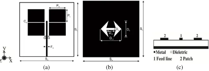
Geometry of the proposed antenna is shown in Fig. 1. The antenna is constructed on an FR-4 substrate with a dielectric constant of 4.4, loss tangent of 0.02 and thickness 1.6 mm. The gap coupled 2×1 array consist of four rectangular patches, where the two patches in the lower layer are driven elements and the two patches in the upper layer acts as parasitic elements with same dimensions printed on the top side of the substrate, A tapered arrow headed dumbbell shaped slot is etched in the ground plane on the other side. The microstrip line and the patches are etched on the top side of the substrate. Figs. 1(a) and 1(b) show the top and bottom view of the proposed design. The simulation and optimization were carried out using CST Microwave Studio. This array configuration shows dual-band operation at 2.45 GHz WLAN band and 3.5 GHz WiMAX band for optimized dimensions. The optimised design parameters of the antenna are as follows (unit: mm), SL = 100, SW = 100, PW = 33.5, PL = 27.6,
G= 3.5, FW = 3.02, Cg = 1,SW1 = 80,SL1 = 50,DL1= 40, DL2 = 18,DW = 4,Dh= 32, R1= 125.
(a) (b) (c)
2.2. Evolution of the Microstrip Patch Array Antenna
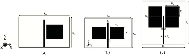
Figure 2 shows the design evolution of the proposed single layer proximity fed microstrip patch array configuration. Initially as in Fig. 2(a) the patch antenna consists of a rectangular radiating patch and a microstrip coupling line. Both the microstrip patch and feed line are printed on top surface of the substrate and a tapered arrow headed dumbbell shaped slot is printed on the ground plane. The microstrip line is placed close to the rectangular patch with a gap G, which capacitively couples the energy to the radiating patch. From the simulation results it is observed that this antenna resonates at 2.89 GHz with a gain of 4.07 dBi. The radiation pattern analysis shows that the beam maxima is 45◦ away from the bore sight. In order to overcome this problem at the next evolution stage another rectangular patch with the same dimensions is placed on the other side of the microstrip feed line as seen in Fig. 2(b). This configuration forms the basic single layer proximity fed 2×1 microstrip patch array antenna. The radiating patches are placed at a distance of 3.5 mm away from the edges of the feed line as shown in Fig. 2(b). The spacing between the nearest edges of the patches is kept atλ/12 and the spacing between the mid-points of the patches is 3λ/8. The microstrip line which is extended beyond the centre of the pair of patches, acts as a tuning stub and it improves the impedance matching of the array antenna. The back side of the substrate has a metallic ground plane with a tapered arrow headed dumbbell shaped slot as seen in Fig. 1(b). The patches are electromagnetically coupled from the feed line and at the same time slot etched in the ground plane enhances the coupling to the radiating patches. The basic 2×1 microstrip patch array configuration is a single band antenna with a centre frequency of 2.791 GHz with an impedance bandwidth of 2.1%. The−10 dB bandwidth for the measured return loss is 68 MHz (2.758–2.826 GHz). The antenna has a measured gain of 6.65 dBi at the resonant frequency with beam maxima along the bore sight direction. In the final stage as shown in Fig. 2(c), additional parasitic elements are gap coupled to the driven elements of the basic 2×1 array antenna to improve impedance bandwidth and to obtain dual-band behaviour. The length of the feed line is optimized to obtain for better impedance matching and length is different from the previous stages. The dimensions of the parasitic patches are same as that of the driven patches. The coupling gap between the parasitic and driven patches is kept at 1 mm on either side.
(a) (b) (c)
Figure 2. Design Evolution of the proposed microstrip patch array antenna.
The basic excitation mechanism of this novel array antenna is that, the driven patches are fed by the microstrip line through electromagnetic coupling and also from the coupling slot fed by the microstrip line. The slot etched in the ground plane enhances the coupling and affect the impedance bandwidth and resonance frequencies. The dimensions of the slot are shown in Fig. 1(b). The slot parameters are optimized to give resonance at frequency of interest in both bands. A variation in any of these parameters will cause either a shift in frequency or degradation in the impedance bandwidth.
(a) (b)
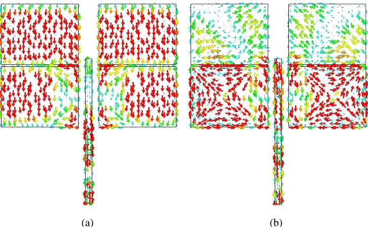
Figure 3. Surface current distribution of the proposed single layer proximity fed gap coupled microstrip patch array antenna (a) at lower resonant frequency and (b) at upper resonant frequency.
can be concluded that at the higher band, driven patches and parasitic patches are clearly divided by current strength and the radiations are mainly from the driven patches.
3. RESULTS AND DISCUSSIONS
A prototype of the proposed proximity fed gap coupled microstrip array antenna based on the optimised dimensions is fabricated and tested. The photograph of the prototype is shown in Fig. 4. The measurement is carried out by using Agilent network analyser E5071C.
(a) (b)
Figure 4. Fabricated prototype of the single layer proximity fed gap coupled microstrip array antenna, (a) top view, (b) bottom view.
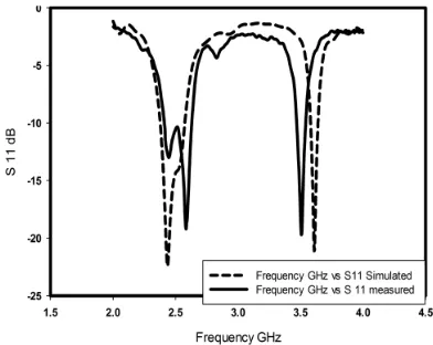
Figure 5. Measured and simulated S11 versus frequency for the proposed proximity fed gap coupled microstrip array antenna.
(a) (b) (c) (d)
Figure 6. Measured radiation patterns (a) E plane for 2.584 GHz, (b) H plane for 2.584 GHz, (c)
E plane for 3.508 GHz and (d) H plane for 3.508 GHz. (co-polarized solid line and cross polarized . . . dashed line).
applications. Even though the upper band of the developed proximity fed gap coupled 2×1 array antenna does not cover the entire WiMAX 3.5 GHz spectrum (3.4–3.6 GHz), but still it can cover the major portion of the WiMAX band with reasonably good gain. The discrepancy between the measured and simulated results may be due to fabrication tolerance.
The measured radiation patterns of the proposed array in the E plane (y-z plane) and H plane (x-z plane) are plotted at the resonant frequencies of 2.584 GHz and 3.508 GHz is shown in Fig. 6.
At the lower band (2.584 GHz) the maximum power was received by the antenna at the bore sight direction while at the upper band (3.508 GHz) the maximum power was received at few degrees away from the bore sight. The upper band characteristics will be found useful in non-line of sight applications including WiMAX. The measured gain of the proposed array is 8.51 dBi at the lower resonant frequency and 5.8 dBi at the upper resonant frequency. It is also observed that in the case of proximity fed gap coupled microstrip patch array antenna the bandwidth in the lower band is enhanced by 217% and the gain is increased by 1.86 dBi when compared basic 2×1 microstrip patch array antenna without parasitic patches.
4. BACK LOBE REDUCTION
(b) (a)
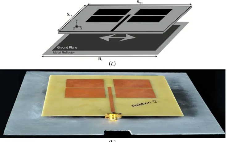
Figure 7. (a) Geometry of the proposed array antenna with reflector metal plate, (b) photograph of the fabricated antenna.
(a) (b) (c) (d)
Figure 8. Measured radiation patterns of the proximity fed gap coupled array antenna with metal plate, (a)E plane for 2.584 GHz, (b)Hplane for 2.584 GHz, (c)E plane for 3.508 GHz and (d)Hplane for 3.508 GHz. (co-polarized solid line and cross polarized . . . dashed line).
which creates an air gap between the substrate and the metal plate. When the gap increases beyond 7 mm the matching degrades. Fig. 7(a) shows geometry of the modified proximity fed gap coupled array antenna with metal plate and the fabricated prototype is shown in Fig. 7(b). The metal plate dimension is optimized as 125×125 mm. The measured gain of the array with metal reflector is 8.79 dBi at the lower resonant frequency and 5.9 dBi at the upper resonant frequency. Plastic screws are used to support the metal plate and dielectric substrate. The Fig. 8 shows the radiation pattern of the modified array with metal plate.
5. BEAM STEERING CAPABILITY
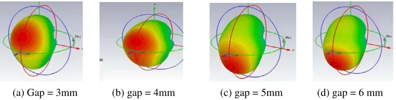
(a) Gap = 3mm (b) gap = 4mm (c) gap = 5mm (d) gap = 6 mm
Figure 9. Three dimensional radiation patterns at lower resonant frequency for various air gaps.
plane and metal plate. The Fig. 9 shows the three dimensional radiation patterns at the lower resonant frequency for various air gaps. Hence pattern reconfigurability is achieved without adding any complex structures.
6. CONCLUSION
A novel single-layer proximity fed gap coupled microstrip patch array that supports WLAN and WiMAX communication services is proposed. In this array configuration driven patches are coupled in close proximity to a centrally placed microstrip line in the same plane along with an arrow headed dumbbell-shape slotted ground plane. Parasitic patch elements are gap coupled to the edges of the driven patches of the array configuration to enhance the bandwidth and gain along with dual-band operation. The array structure is modified by placing a metal reflector plate at the back side of ground plane to improve front to back ratio. By mechanically varying the air gap between the ground plane and metallic reflector, pattern reconfigurable antenna characteristics are achieved.
ACKNOWLEDGMENT
The authors would sincerely express the gratitude to Mr. Sathyan Balakrishnan, Spectrum Antenna and Avionics systems (P) Ltd. Kochi, Kerala, India for providing the measurement facilities.
REFERENCES
1. Khan, M. U., M. S. Sharawi, and R. Mittra, “Microstrip patch antenna miniaturisation techniques: A review,” IET Microwaves, Antennas and Propagation, Vol. 9, No. 9, 913–922, 2015.
2. Lee, K. F. and K. F. Tang, “Microstrip patch antenna — Basic characteristics and some recent advances,”Proceedings of the IEEE, Vol. 100, 2169–2180, July 2012.
3. Chang, T. N. and J. H. Jiang, “Enhance gain and bandwidth of circularly polarized microstrip patch antenna using gap coupled method,” Progress In Electromagnetics Research, Vol. 99, 127– 139, 2009.
4. Deshmukh, A. A. and G. Kumar, “Compact broad band gap coupled shorted square microstrip antennas,”Microwave And Optical Technology Letters, Vol. 48, 1261–1265, 2008.
5. Meshram, M. K. and B. R. Vishvakarma, “ Gap-coupled microstrip array antenna for wide-band operation,” International Journal of Electronics, Vol. 88, No. 11, 1161–1175, 2001.
6. Aanandan, C. K., P. Mohanan, and K. G. Nair, “Broad band gap coupled microstrip antenna,” IEEE Transactions On Antennas And Propagation, Vol. 38, No. 10, 1581–1586, 1990.
7. Wei, K., Z. Zhang, and Z. Feng, “New coplanar capacitively coupled feeding method for circularly polarized patch antenna,” IEEE Antennas and Propagation Society International Symposium, 3099–3102, Spokane, USA, 2011.
9. Tu, Z. H., Q. X. Chu, and Q. Y. Zhang, “High gain slot antenna with parasitic patch and windowed metallic substrate,” Progress In Electromagnetics Research Letters, Vol. 15, 27–36, 2010.
10. Deshmukh, A. A. and K. P. Ray, “Proximity fed gap-coupled half E shaped microstrip antenna array,”Sadhana-Indian Academy of Sciences, Vol. 40, 75–87, 2015.
11. Lai, H. W., K. M. Mak, and K. F. Chan, “Novel aperture coupled microstrip line feed for circularly patch antenna,” Progress In Electromagnetics Research, Vol. 144, 1–9, 2014.
12. Majid, H. A., M. K. A. Rahim, M. R. Hamid, and M. F. Ismail, “Frequency reconfigurable microstrip patch slot antenna with directional radiation pattern,” Progress In Electromagnetics Research, Vol. 144, 319–328, 2014.
13. Costantine, J., Y. Tawk, J. Woodland, N. Flaum, and C. G. Christodouloues, “Reconfigurable antenna system with a movable ground plane for cognitive radio,” IET Microwave antennas and propagation, Vol. 8, No. 11, 858–863, 2014.
14. Ali, M. T. and M. N. M. Tan, “A novel of reconfigurable planar array (RPAA) with beam steering control,” Progress In Electromagnetics Research B, Vol. 20, 125–146, 2010.
15. Sami, B., B. Randa, S. Benkouda, and T. Fortaki, “Full-wave analysis of anisotropic circular microstrip antenna with air gap layer,” Progress In Electromagnetics Research M, Vol. 34, 143– 151, 2014.