z
RESEARCH ARTICLE
STRUCTURAL AND OPTICAL PROPERTIES OF NANOSTRUCTURED POROUS SILICON FOR
ETHANOL GAS SENSING APPLICATION
1
Kavu Kulathuraan,
2Venkatasamy Ramadas and
3*Balan Natarajan
1
Department of Physics, A.P.A College of Arts and Culture, Palani-624 601, Tamil Nadu, India
2Department of Zoology, R.D Government Arts College, Sivagangai-630561, Tamil Nadu, India
3Department of Physics, R.D Government Arts College, Sivagangai-630 561, Tamil Nadu, India
ARTICLE INFO ABSTRACT
Porous Silicon (PS) layers were prepared by electrochemical etching in a single-tank cell on the surface of single-crystalline p-type (100) silicon wafers, using hydrofluoric acid (HF) and ethanol (C2H5OH) in the volume ratio of 1:2. The surface and cross-section morphologies of the PS were observed from images obtained using Scanning Electron Microscope (SEM). Likewise, the porosity of the PS sample was determined using the parameters obtained from SEM images by geometrical method. SEM images indicated that, the pores were surrounded by a thick columnar network of silicon walls. This porous silicon layer can be considered as a sponge like structure. The X-ray diffraction (XRD) pattern showed the growth of PS layer on silicon wafer and the grain size of the PS layer was found to be around 60.2 nm. The effective refractive index of porous silicon was calculated using Effective Medium Approximation (EMA) analysis. The optical properties of PS were investigated using Fourier Transform Infrared (FTIR) spectroscopy and Photoluminescence (PL). The surface chemical bonds of the PS were observed by FTIR and the band gap of the PS sample was obtained from PL spectra. The efficiency of ethanol gas sensing properties of PS was investigated at room temperature. The sensor was found to operate with maximum efficiency at a concentration of 100 ppm hence, this PS material can be used as an effective sensor element to detect ethanol vapour.
Copyright © Kavu Kulathuraan et al. This is an open access article distributed under the Creative Commons Attribution License, which permits unrestricted use, distribution, and reproduction in any medium, provided the original work is properly cited.
INTRODUCTION
Porous silicon (PS) is electrochemically produced by anodic dissolution of crystalline silicon in a hydrofluoric acid solution. The visible photoluminescence of PS at room temperature reported by Canham (1990) and which has attracted a significant interest due to the prospect of manufacture of an integrated optical device on silicon (Canham 1990; Kaneko
et al., 1993). The pore size has been classified as microporous, mesoporous and macroporous. The porosity is defined as the fraction of the apparent volume attribute to pores is larger for microporous. PS layers with high porosity have potential applications in light emitting diodes, anti-reflection coating and non-linear optics, medium porosity in micromachining, sensors, silicon on insulator, low porosity in micro capacitors, wafer bonding, etc. (Balagurov et al., 1997; Ming-Kwei Lee
et al., 2001; Nenad Lalic et al., 1996; Iraji zad et al., 2004;
Leigh Canham 1997). Recently, an increasing interest on the sensing properties of PS material has emerged. Its ability to react with gases and sense them eagerly is related with the large surface to volume ratio (Iraji zad et al., 2004). Organic vapour sensitivity in a PS device employing semiconductor
*Corresponding author:Balan Natarajan
Department of Physics, R.D Govt. Arts College, Sivagangai-630 561, Tamil Nadu, India.
technology, with a detection limit of approximately 1000 ppm for ethanol has also been reported (Watanabe et al., 1995). The physical properties of PS sample, like the electrical resistance, have been observed to change in presence of humidity, organic vapours and contaminants like NO, NO2, CO2. The advantages
of PS gas sensors compared with metal oxide gas sensors are: low cost, low power consumption and room temperature operation. The aim of this paper is to study the structural and optical properties of nanocrystalline porous silicon based ethanol gas sensor in lower concentration at room temperature.
MATERIALS AND METHODS
Porous silicon samples were prepared by conventional electrochemical dissolution in a single-tank cell on the surfaces of single-crystalline p-type silicon (100) substrates (250±0.5μm thickness, 0.5–3.0 ohm cm resistivity). The anodizing solution was obtained by mixing of HF (48 vol. %) with ethanol in the volume ratio of 1:2, and the etching was carried out with a current density of 100mA/cm2 for 30 minutes (etching time) duration. In order to remove the native oxide, the sample was placed in the etching solution for 1 minute prior to the etching. After anodization, the electrical connections were made using fine copper wire and silver paste for the metallization contacts on the porous silicon layers to obtain the PS based sensing
ISSN: 0975-833X
Available online at http://www.journalcra.com
International Journal of Current Research Vol. 6, Issue, 01, pp.4511-4515, January,2014
INTERNATIONAL JOURNAL OF CURRENT RESEARCH
Article History:
Received 11th September, 2013
Received in revised form 20th October, 2013
Accepted 10th December, 2013
Published online 26th January,2014
Key words:
Microporous materials, Nanostructures, Electrochemical etching, Scanning electron microscopy, X-ray diffraction,
device. The surface morphology and cross sectional view of the PS sample were obtained using a Scanning Electron Microscope (SEM, Hitachi, model S-3000N). The X-ray Diffraction (XRD) spectra were recorded using Bruker D8 advanced X-Ray Diffractometer using CuKα1 (1.54060Ao) as a
source. The surface chemical bonds of the PS were studied by Fourier Transform Infrared Spectoscopy (FTIR, NEXUS470). The Photoluminescence (PL) excitation spectra were obtained using a Shimadzu RF 5301 Luminescence Spectrophotometer. A pulsed xenon lamp was built in the spectrophotometer as the excitation source. The ethanol gas sensing characteristics of PS sample was measured at room temperature using an electrometer (6517A, Keithley, USA) connected to Volatile Organic Compound (VOC) testing chamber with a capacity of 3 L. Test gas was precisely inserted using an injector.
RESULTS AND DISCUSSION
Structural Analysis
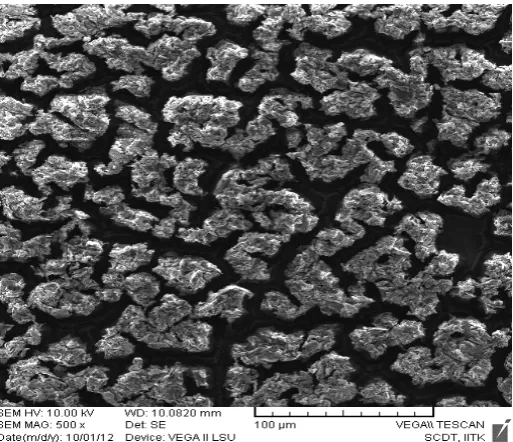
SEM morphology of porous silicon formed at HF: ethanol concentration in the volume ratio of 1:2 has been indicated in Figure - 1(a). It can be seen that, the uniform distribution of large sized pores was observed along with quantum sponge structure in the thick columnar network of silicon walls. Observation of these micro structures may be taken to indicate the formation of nano-crystalline silicon particles inside and all over the etched layer which gave good photoluminescence at room temperature. The porosity plays an important role in photoluminescence properties of porous silicon layer. The porosity of porous silicon can be defined as the quantity of silicon removed during anodization compared with the silicon concentration before anodization evaluated in the same volume. The porosity can also be defined as a function of geometrical parameters and written as (Salcedo et al., 1997; Kulathuraan et al., 2012),
2
1 1 732 . 1 * 2
d m
P
(1)Where….
d is the average pore size and m is the distance between pores.
Using the above equation, we have estimated the porosity of our PS is 62%.
The SEM image of the cross sectional view of the porous silicon sample is depicted in Figure - 1(b). The pore with a straight parallel channel was perpendicular to the substrate. The structure of the pore is regular and spongy in nature near the top surface. The thickness of the PS layers was measured from SEM cross section views and recorded as 9.8 μm. The refractive index of a PS layer is related to its porosity found by the Bruggeman effective medium approximation (Thei 1996).
Figure-1(a). Scanning Electron Micrographs of Porous Silicon (PS)
Figure-1(b). SEM cross-section morphology of Porous Silicon (PS)
[image:2.595.308.565.52.273.2] [image:2.595.306.562.323.609.2]Figure 2. XRD pattern of Porous Silicon (PS)
The presence of a strong peak at 69.3o was the (400) reflection of the silicon crystal which indicated the formation of pores in the silicon surface. This is the first allowed peak in the (100) oriented c-Si and weak peak at 47.3o and 56.1o. These peaks correspond to (200) and (320) planes of c-Si, respectively. The presence of narrow peak around 28.4o might probably be due to the presence of amorphous silica in the PS sample. This value agrees reasonably well with the value of an amorphous silica plate (Prabakaran et al., 2002). The full width at half maximum (FWHM) of all the peaks was large, which may be attributed to the roughness of PS surface (Wang et al., 2007). The average particle size was obtained as 60.2 nm calculated from Debye– Scherrer formula (Khranovskyy et al., 2006).
cos
9
.
0
D
(2)Where ..
D is the diameter of the crystallites forming the PS, λ is the wavelength of CuKa line (0.15406 nm),
β is full width at half maximum (FWHM) in radian and
θ is Bragg angle.
FTIR spectra
The FTIR spectrum of the PS sample is depicted in Figure - 3. The strong absorbance peaks were observed at 1111cm-1 and weak peaks of lower intensities were also observed at around 2079 cm-1 and 904 cm-1. The strong peak observed at 1111 cm
-1
band was due to the Si-O-Si stretching mode as indicated in Table - 1. The weaker band at 904 cm-1 is connected with hydrogen bonding SiH2 at the surface of PS and the doublet at
around 2079 cm-1 has been identified as SiHn. The small
doublet at 618 cm-1 can be assigned to SiH wagging mode and these observations were indicated in Table - 1.
[image:3.595.317.556.52.217.2]Figure 3. FTIR spectra of Porous Silicon (PS)
Table - 1. Observed surface bonding in the Porous Silicon (PS) (Using FTIR spectra)
Wave number (cm-1) Bonds Vibration mode
2079 Si-H2 Stretch
1111 Si-O-Si Sym-stretch 904 Si-H2 scissors
618 Si-H (or) Si-H2 Wag (or) deformation
The presence of hydrogen complexes (SiH, SiH2, and SiHn)
was suggested to explain the luminescence of PS (Zhang 1991; Sailor et al., 1997). The experimental and theoretical investigations of several workers (Papaconstantopoulos and Economou 1981; Ching et al., 1980; Freeman and Paul 1979; Cody et al., 1980; Goodman et al., 1980) have established that the hydrogenation not only eliminates the dangling bond states from the energy gap, but also widens the energy gap. Thus, the chemisorptions of Si-Hn from PS appear to be closely linked to
a sharp increase in the PL intensity of PS. The results of the present study also indicated that SiHn plays a key role to the
observed luminescence process.
Photoluminescence Studies
Photoluminescence spectra were obtained at room temperature under the excitation of 450 nm light and the PL spectra of the freshly prepared PS at constant current density of 100mA/cm2 were shown in Figure - 4(a). The emission peak was absorbed at 605 nm; and the porous silicon film has its internal surface covered with Si-Hn bond, with tie up the dangling bands. It
provides a very good passivation of the defects and allows very attractive efficiency to be obtained. The occurrence of strong PL spectra at room temperature in the visible range may be attributed to the transitions among the quantum-confined states in the nanoscale Si, which are influence by the surface bond (Zhang 1991). The band gap value was estimated as 1.97 eV for PS. The extracted values of band gap were in the same range of the reported results (1.52.5 eV) for PS samples (Rajabi and Dariani 2009; Sheng et al., 2008; Srinivasan et al., 2007).
[image:3.595.320.544.283.337.2]
Figure-4(a). Photoluminescence spectra of Porous Silicon (PS)
Figure-4(b). Ethanol gas sensing properties of Porous Silicon (PS) in 100 ppm at room temperature
Gas sensing properties of Porous Silicon (PS)
The gas sensing properties of the PS towards ethanol (C2H5OH) was tested at room temperature. The change in
surface resistance of the PS was recorded using electrometer (Model 6517A, Keithley, Germany) in the presence of 100 ppm of ethanol and is shown in Figure - 4(b). It can be seen that the resistance values of PS gas sensors initially decrease to stable values when adsorbing ethanol gas, after disengagement from the gas environment, the resistance values increase gradually to stable values. As ethanol is a reducing gas, it makes local and fully reduction of PS surfaces which causes the decrease of defect density. These defects play a role in electron traps into which electrons relax (Razi, et al., 2008; Xie And von Blanckenhagen 1999; Okamoto and Kanemitsu 1996). The decrease of the number of electron traps will induce a large number of free electrons on the surfaces of PS and the number of holes reduced greatly, so that resistance values decreases. Therefore, it seems that, the electrons traps which are diminished by full reduction of PS in the presence of ethanol gas are responsible for the decrease of free charge carriers in p-type PS. The sensitivity (S) is found to be 211×103 using the Eq. 3:
Rb
Rb
Ra
S
(3)Where,
Ra is the electrical resistance of the PS in the absence of
ethanol vapour and
Rb is the electrical resistance of the PS in the presence of
ethanol vapour.
Response and recovery time of the PS was between 5168 and 4693 sec, respectively.
Conclusion
Porous silicon sample was successfully prepared by electrochemical etching technique in a single-tank cell setup. SEM micrographs showed uniform distribution particles in PS with quantum sponge like structure in the thick columnar network of silicon walls. The thickness of the PS layer was 9.8 μm which was confirmed by SEM cross section views. The effective refractive index of a PS was calculated by the Bruggeman effective medium approximation. The average particle size of PS was calculated by x-ray diffraction pattern. Visible PL was observed at 605 nm for PS sample and which exhibits a PL band at red region, suggesting that hydride related luminescence process may be active in PS. The band gap energy value of PS was calculated from PL spectra. The occurrence of a strong PL & FTIR spectra may be attributed to the transition among the quantum confined states in nanoscale Si, which are influenced by the surface bonds. The XRD and PL studies confirm the presence of silicon nanocrystallites and networks in the PS structure. Sensing performance of the PS was studied with exposure of 100 ppm of ethanol gas at room temperature. The response was found to be 211×103.
REFERENCES
Balagurov L.A., D.G. Yarkin, G.A. Petrovicheva, E.A. Petrova, A.F. Orlov, S.Ya. Andryushin, 1997. “Highly
sensitive porous silicon based photodiode structures,”
J. Appl. Phys. 82, 4647.
Bsiesy A., Y.F. Nicolau, A. Ermolieff, F. Muller, F. Gaspard, 1995. “Electroluminescence from n+-type porous silicon contracted with layer-by-layer deposited polyaniline,” Thin
Solid Films, 255, 43.
Canham, L.T. 1990. “Silicon quantum wire array fabrication by electrochemical and chemical dissolution of wafers,” Appl.
Phys. Lett. 57, 1046.
Ching W. Y., D. J. Lam and C. C. Lin, 1980. “Electronic states and bonding configurations in hydrogenated amorphous silicon,” Phys. Rev. B, 21, 2378.
Cody G. D., C. R. Wronski, B. Abeles, R. B. Stephens and B. Brooks, 1980. “Optical Characterization of Amorphous Silicon Hydride Films,” Sol. Cells, 2, 227.
Freeman and W. Paul, E. C. 1979. “Optical constants of rf sputtered hydrogenated amorphous Si,” Phys. Rev. B, 20, 716.
Iraji zad, F. Rahimi, M. Chavoshi, M.M. Ahadian, A. 2004. “Characterization of porous poly-silicon as a gas sensor,”
Sensor. Actuat. B, 100, 341.
Isabel Ferreira, Elvira Fortunato, Rodrigo Martins, 2004. “Ethanol vapour detector based in porous silicon a-Si:H films produced by HW-CVD technique,” Sensor. Actuat. B 100, 236-239.
Kaneko H., P.J. French, R.F. Wolffenbuttel, 1993. “Photo and Electro-luminescence from Porous Si,” J. Lumin. 57, 101. Khranovskyy, V., Grossner, U., Nilsen, O., Lazorenko, V.,
Lashkarev, G.V., Svensson, B.G. and Yakimova, R. 2006. “Structural and morphological properties of ZnO:Ga thin films,” Thin Solid Film, 515, 472-476.
Kulathuraan K., J. Pandiarajan, N. Prithivikumaran, N. Jeyakumaran and B. Natarajan, 2012. “Structrual and Optical properties of Polymer Composities/Porous Silicon,”
AIP Conf. Proc. 215, 1451.
Leigh Canham, 1997. “Properties of Porous silicon,” EMIS
datareviews seriesno. 18.
Ming-Kwei Lee, Chi-Hsing Chu, Yu-Hsing Wang, S.M. Sze, 2001. “1.55-µm and infrared-band photoresponsivity of a Schottky barrier porous silicon photodetector,” Opt. Lett. 26, 160-162.
Nenad Lalic, Jan Linnros, 1996. “A porous silicon light-emitting diode with a high quantum efficiency during pulsed operation,” Thin Solid Films, 276, 155-158.
Okamoto S. and Y. Kanemitsu, 1996. “Photoluminescence properties of surface-oxidized Ge nano crystals: surface localization of exitons,” Physical Review B, 54, 16421– 16424.
Papaconstantopoulos D. A. and E.N. Economou, 1981. “Calculations of the electronic properties of hydrogenated silicon,” Phys. Rev. B., 24, 8233.
Prabakaran R., G. Raghavan, S. Tripura Sundari, R. Kesavamoorthy, 2002. “Ellipsometry studies on the effect of etching time in porous silicon,” Physica E, 15, 243-251. Rajabi M. and R. Dariani, 2009. “Current improvement of
porous silicon Photovolatic devices by using double layer porous silicon structure: applicable in porous silicon solar cells,” J Porous Mat, 16, 513 – 519.
Razi, F.; Rahimi, F., Zad, A.I. 2008. “Fourier transform infrared spectroscopy and scanning tunneling spectroscopy of porous silicon in the presence of methanol,” Sensor
Actuat. B-Chem. 132, 40.
Sailor M. J., J. L. Heinrich Jr and Laurerhans, 1997. “Luminescent porous silicon: Synthesis, chemistry, and applications,” Stud. Surf. Sci. Catal., 103, 209.
Salcedo W.J., F.J. Ramirez Fernandez, E. Galeazzo, 1997. “Structrual Characterization of Photoluminescent Porous Silicon with FTIR Spectroscopy,” Brazilian Journal of
Physics, 27,158–161.
Sheng C.K., W. Mahmood Mat Yunus, W.M.Z.W. Yunus, Z. Abidin Talib and A. Kassim, 2008. “Characterization of thermal, optical and carrier transport properties of porous silicon using the photoacoustic technique,” Physica B, 403, 2634-2638.
Srinivasan, R., M. Jayachandran and K. Ramachandran, 2007. “Photoacoustic studies on optical and thermal properties of p-type and n-type nanostructured porous silicon for (100) and (111) orientations,” Cryst Res Technol, 42, 266-274. Thei W., 1996.“The dielectric function of porous silicon – how
to get it and how to use it,” Thin Solid Films, 276, 7–12. Wang C.F , Li Q S, Zhang L C, Lu L and Qi H X 2007,
Optoelectron. Lett,. 3 0169.
Watanabe K., T. Okada, I. Choe, Y. Satoh, 1995. “Organic vapour sensitivity in a porous Si device,” Proc.
Eurosensors IX (1), 890–893.
Xie, F.Q.; von Blanckenhagen, P. 1999. “Observation of harmonic current oscillations on partially oxidized Si(111) surfaces by scanning tunneling microscopy,“ Appl. Phys.
Lett., 75, 3144.
Zhang X. G. 1991. “Mechanism of Pore formation on n-type silicon,” J. Electrochem. Soc., 138, 3750.
Zhang X. G., 1991. “Mechanism of pore formation on n-type silicon,” J. Electrochem. Soc., 138, 3750.