Wafer Defect Detection Using Directional
Morphological Gradient Techniques
Gongyuan Qu
Electrical Engineering Department, Santa Clara University, Santa Clara, CA 95053, USA Email: [email protected]
Sally L. Wood
Electrical Engineering Department, Santa Clara University, Santa Clara, CA 95053, USA Email: [email protected]
Cho Teh
Electrical Engineering Department, Santa Clara University, Santa Clara, CA 95053, USA Email: [email protected]
Received 30 July 2001 and in revised form 12 March 2002
Accurate detection and classification of wafer defects constitute an important component of the IC production process because together they can immediately improve the yield and also provide information needed for future process improvements. One class of inspection procedures involves analyzing surface images. Because of the characteristics of the design patterns and the irregular size and shape of the defects, linear processing methods, such as Fourier transform domain filtering or Sobel edge detection, are not as well suited as morphological methods for detecting these defects. In this paper, a newly developed morphological gradient technique using directional components is applied to the detection and isolation of wafer defects. The new methods are computationally efficient and do not rely on a priori knowledge of the specific design pattern to detect particles, scratches, stains, or missing pattern areas. The directional components of the morphological gradient technique allow direction specific edge suppression and reduce the noise sensitivity. Theoretical analysis and several examples are used to demonstrate the performance of the directional morphological gradient methods.
Keywords and phrases:morphological gradient, edge detection, edge orientation, wafer inspection.
1. INTRODUCTION
With the increasing gate density of very large scale integra-tion (VLSI) designs, defects in a wafer are more likely to cause failures of chip production and lower yields, which is a significant problem considering the substantial financial in-vestment in fabrication plants. Intensive defect control pro-cedures during integrated circuit (IC) production can help improve yields in several ways. Early detection of defects can be used to predict the yield. For wafers that have so many defects that the predicted yield would be unacceptably low, further processing can be terminated. In addition, analysis of the defects to identify the type and probable sources can be used to improve the production process. A great variety of process defects may occur over all technological steps in VLSI and application specific integrated circuit (ASIC) pro-duction. Well-known examples are oxidation stacking faults, spikes, residues from chemicals, etching defects, and different kinds of particles [1]. This paper applies detection methods
to defects that result in scratches or spots due to particles, stains, or missing pattern areas.
A variety of methods and technologies have been applied to defect inspection of wafers [1, 2, 3, 4, 5, 6, 7, 8, 9]. Vi-sual inspection with a microscope can take advantage of an experienced operator’s ability to detect and classify defects. However, effective automated analysis is more desirable be-cause it can be scaled up to the desired level of testing with-out exhausting the limited resource of human inspectors. In addition, different inspectors will make different judgments in some cases, and this may cause inconsistent feedback for process improvement.
If the specific design is known, then design rule checking or image comparison may be used. However a more general technique can be based on the known design feature size of the technology and the expected characteristics of the defects. Driven by shrinking design rules, the traditional opti-cal imaging detection technologies have limited capability to detect physical defects within high aspect ratio struc-tures and electrical defects within interconnect strucstruc-tures [10]. Electron beam technology overcomes the limitation of resolution, depth of focus, and the detection of subsurface interconnect structure defects, and it is now moving onto the production floor. With the new copper process emerg-ing, scanning electron microscope (SEM) review stations have become essential and integral parts of wafer production [11, 12, 13]. In addition, the adoption of 300 mm wafer pro-duction has made automation an obligatory requirement. It is no longer sufficient to simply detect 10,000 defects; most production requires the defects to be classified automatically to quickly determine the root cause. Thus automatic defect classification (ADC) has become a mandatory option in in-spection and review stations [14, 15, 16, 17, 18, 19]. For the purpose of detecting defects without losing throughput, in-line automatic defect classification (IADC) or even on the fly (OTF-ADC) defect classification are required for deposition of bad wafers at an early stage. Furthermore, the root of cause of the defect or the defect source identification becomes im-portant for locating the source of the defect, defect elimina-tion, and the prediction of yield [8, 20, 21, 22, 23, 24, 25].
Defect detection and classification may be accomplished in multiple stages [2]. Early detection may rely on simply subtracting the image from an aligned reference image and treating any difference as a defect. The location of these po-tential defects can be used by a later analysis stage to extract the geometric features of defects, including size, shape, and orientation. Edge detection operators are usually applied to obtain this information [2, 26, 27, 28, 29, 30]. The Sobel op-erator and the first or the second order differential opop-erators such as the Laplacian of Gaussian (LOG) are well understood and often used for this purpose. However, for several reasons these methods are not well matched to the detection of de-fects with irregular size, shape, and edges in the context of regular high-contrast geometric patterns. These differential operators will amplify noise in the image [26, 27, 28, 29], and their response to irregular defect edges will be weak com-pared to the design pattern response. A first stage of low pass filtering can be used to reduce noise and to suppress the sharp edges of the design features, but this weakens the less distinct edges of the irregular defects even more. Morphological fil-ters may also be used in this processing [2, pages 117–119], [29], but the conventional morphological gradient operator does not provide edge orientation information which may be needed for detection of scratches. The morphological gradi-ent also has a higher noise sensitivity than the Sobel operator [31, 32, 33, 34].
In this paper, directional morphological gradient opera-tors are defined [33, 34] and then applied to defect detection. The proposed operators detect edges and provide both edge strength and edge orientation information. The sensitivity to
noise is significantly reduced compared to the simple phological gradient. In addition, the properties of the mor-phological filter allow it to respond to defects of different sizes and irregular shapes even if they are blurred by prepro-cessing. The performance of the proposed operator is com-pared with the Sobel, LOG [35], and Canny [36] operators for several wafer defect images. It has been assumed that the image acquisition process will produce design pattern com-ponents with a pixel dimension of approximately three or four to avoid oversampling while guaranteeing adequate res-olution. It is also assumed that the defects are larger than the design feature dimension, irregular in shape, and positioned randomly with respect to the design pattern. Since these as-sumptions are based on measures relative to pixel dimen-sions, this method can continue to be used, as design fea-ture size is further reduced and circuit density is increased as long as effective image acquisition can be accomplished. The experimental results for scratch and spot defects show that proposed operators can detect these defects and suppress the design pattern to allow geometric shape analysis of the de-fects. The proposed morphological gradient technique using directional components discussed in this paper is well suited for defect redetection and ADC for review stations.
2. GRAY SCALE MORPHOLOGICAL GRADIENT
OPERATORS
2.1. Gray scale erosion and dilation
The basic operations for morphological filtering are erosion and dilation [31, 37]. LetF = f(x, y) be a gray scale im-age of domainDf, and letB = b(x, y) be a structuring el-ement of domain Db, where xand y are the pixel indices. The structuring element has a size and shape appropriate for the geometric features of interest. For a structuring element (SE) with positive values, the dilation operation enlarges the bright image areas while reducing the darker areas. Erosion has the opposite effect. The dilated gray scale image fd(x, y) and the eroded image fe(x, y) are defined by (1) and (2),
re-When a structuring element has a constant value of zero over its domain, it is called a flat structuring element [31]. When a flat structuring element is used in (1), the dilated image value at each pixel position is the maximum of all the pixel values of the original image over a region defined by
the pixel values in a region defined byb(x, y) shifted to that pixel position. All values in the dilated and eroded images are values of some pixel in the original image. Using (1) and (2), we define (3) and (4) as the dilated and eroded images for the special case of a flat structuring element:
fd(x, y, B)=max
The dilated and eroded images can be computed by scan-ning the list of pixel values for each shifted position of the structuring element domain and determining the maximum and minimum values in the list. When a large structuring el-ement can be created by a sequence of dilations using smaller structuring elements, the dilation and erosion computation can also be implemented as a sequence of dilation or erosion operations using the smaller structuring elements. This de-composition property, or chain rule, is defined in (5) and (6) [31]. Let the structuring elementB3be formed by the dilation of two smaller structuring elementsB1andB2. Then dilation or erosion withB3can be implemented with sequence of the corresponding operations usingB1andB2:
squares, then the domain ofB3would be a 3×3 pixel square. A roughly circular structuring element can be created with a sequence of dilations alternately using a square and diamond shaped structuring element. This method can be advanta-geous for hardware implementations and is efficient when the intermediate products or multiple sizes for structuring elements are needed.
2.2. Morphological gradients
The difference between the dilated image and the eroded image can be defined as the basic morphological gradient
gm(x, y, F, B) given by (see [37])
gm(x, y, F, B)= fd(x, y, B)−fe(x, y, B). (7)
For a flat structuring element, the value of this gradient will always be nonnegative, so it cannot be used to distinguish between rising and falling edges. Variations of this defini-tion include the erosion residue and the diladefini-tion residue defined, respectively, as the difference between the original image and the eroded image, and the difference between the dilated image and the original image [28, 29]. If the foreground object is brighter than the background, then the dilation residue pushes the edges of the object outward while the erosion residue pushes the edges inward. Further
variations of these methods, which are defined to avoid biases in the position of the edges [38], include gradients defined as the maximum, the minimum, and the average of the ero-sion and dilation residues. Because the eroero-sion residue and dilation residue edges are offset in different directions, the minimum of the two will be zero for very sharp edges. Thus, some blurring is necessary for effective use of the minimum residue.
The erosion and dilation operations capture the extreme values within a neighborhood defined by the structuring element. This allows these operators to be effective for ir-regular objects, but it also results in sensitivity to noise [34, 38, 39]. Noting this, many investigators have proposed improvements to reduce the noise sensitivity [38, 39]. The blur-minimum-operator (BMO) proposed by Lee [38] first blurs the imagef(x, y) with blurring functionhs(x, y) to cre-ate fs(x, y) and then computes the gradient as the minimum of the erosion and dilation residues of the blurred image. This operation is defined as
gBMO The blurring suppresses high frequency noise and spreads sharp edges so they will not be missed when the minimum is taken. Because the minimum of the residues is used, this op-erator will usually have a significantly weaker response than the basic morphological gradient defined by (7).
3. DIRECTIONAL MORPHOLOGICAL GRADIENTS
The orientation of an edge segment can be used by higher level segmentation processes to make decisions about con-necting adjacent edge segments with compatible orientations to form a boundary or rejecting edge segments that are in-consistent in orientation estimates. For example, the Canny edge detector uses two thresholds and accepts edge segments at the lower threshold only when they are connected to edges at the higher threshold [36]. In applications such as defect detection for wafer inspection, the orientation of the edge may be as significant an indicator for defect isolation as the edge magnitude.
Operators such as the Sobel and Prewitt operators deter-mine orientation information by separately computing hor-izontal and vertical differences. The Sobel operator uses the two linear separable filters defined by the vector outer prod-ucts, 0.25·[1 2 1]T ·[1 0 −1] and 0.25·[1 0 −1]T · [1 2 1], to create two orthogonal difference components at each pixel location. These components are interpreted as vec-tor components to compute a gradient magnitude and an-gle for each pixel position. The Robert’s cross computation is similar except that a 2×2 region is used instead of a 3×3 region.
0 0 0
Figure1: Four flat one-dimensional structuring elementsBθ,lfor l=3 at orientationsθ=0,π/2,π/4, and 3π/4.
analysis, we adopt the notation of (9) to represent either type of directional morphological gradient,
g(x, y, F, B,op)=
3.1. DMG and DBMO operators
The directional morphological gradient operator uses sev-eral one-dimensional flat structuring elements [32, 33, 34]. Let these structuring elements be called Bθ,l, wherelis the length of the structuring element in pixels andθis the orien-tation. To have overlapping center reference points,lshould be an odd integer. The four structuring elements of length 3 shown in Figure 1 provide horizontal, vertical, and diagonal domains. The gradient component values for each direction are calculated using (10), with gradient operators defined in (9),
There are two major advantages of using several one-dimensional structuring elements to compute morphologi-cal gradients. One is to produce orientation information in a manner similar to the Sobel and other related operators. An-other is to reduce the noise sensitivity, which increases as the size, in pixels, of the structuring element increases [32, 34]. The four separate SEs of sizelwill have a lower noise sensi-tivity than one SE of sizel2. Whenl=3 and the four angles 0,π/4,π/2, and 3π/4, are used, all pixels in a 3×3 neigh-borhood can contribute to the gradient calculation. A third advantage when using four rather than two SE orientations is that the two angle estimates can be combined to give a more accurate orientation estimate than the Sobel operator. The two angle estimates also allow additional noise suppression capability if incompatible estimates are taken as an indica-tor of noise, and the corresponding segment may be rejected even when the edge magnitude is significant.
3.2. Application to ideal step edge and constant gradient models
Although using the one-dimensional structuring elements to create directional components for morphological gradi-ent methods is similar in approach to the Sobel and related methods, the computation of the magnitude and the orienta-tion of the morphological gradient requires a method differ-ent from the vector compondiffer-ent method. This will be devel-oped by first considering the response to a noiseless constant
gradient image. Then an ideal step edge at arbitrary orien-tation and offset from the pixel grid axes will be considered. It will be assumed that the aperture function of the image acquisition device is known. An example of these two edge models is shown in Figure 2. Figure 2a shows an ideal step edge and Figure 2c shows a surface with a constant gradient. These two edge models are applicable to defect detection be-cause the design pattern will consist primarily of sharp well-defined edges. Defects will generally be less well well-defined, and defect boundaries may be similar to the gradual ramp model. Application examples will demonstrate the importance of ac-curate and consistent angle estimation made by the direc-tional morphological gradient when used to determine the orientation of scratches.
A constant gradient source can be modeled by the con-tinuous function
s(x, y)=s0+a
x(cosθ) +y(sinθ), (11)
for continuous variablesxandy. This represents a ramp sur-face with the parameteradetermining the slope and the pa-rameterθdetermining the direction of the steepest change. The constants0is the value at the origin of thex-ycoordinate system. If the aperture function of the image acquisition sys-tem is symmetric, the acquired digital image, f(x, y), will be a scaled copy ofs(x, y) for values ofxandycorresponding to pixel centers. For this image model, the horizontal and verti-cal components from the Sobel operator will be 2acos(θ) and 2asin(θ). These values are independent of the coordinatesx
andybecause the constant gradient model has no localiza-tion to any specific posilocaliza-tion. A magnitude of 2aand an an-gle ofθwill be computed from the two vector components. Using (3), (4), and (7) for a DMG with two perpendicular structuring elements of length 3, the gradient components areg0,3 = |2acos(θ)|andgπ/2,3 = |2asin(θ)|. Both the So-bel operator and the morphological gradient results are in-dependent of the constant offset values0.
From the definitions of (3), (4), and (7), a morphologi-cal gradient component value must always be a nonnegative difference between a maximum and minimum value over a region specified by the structuring element. Clearly, from these two components, an angle and a magnitude could be computed using the same vector interpretation of the com-ponents as the Sobel method. However, without the sign in-formation, the angle could be in any of the four quadrants. The DBMO gradient is computed in the same manner. If its smoothing is symmetric the constant gradient image will not be changed by the smoothing operation. The component values will be half of the DMG component values because the minimum residue is used. When the length of the struc-turing element, l, is increased, the angle estimated by both the DMG and DBMO for the constant gradient image will not change. The magnitude computed by the DMG will be
a∗(l−1). When comparing the performance of gradient es-timators, all are normalized to provide a unit output for a vertical ideal step edge.
0
Figure2: Images of mathematical models for step edge (a) and con-stant gradient image (c) when the angle isπ/6. Small aperture blur-ring of (a) results in the model shown in (b). The result of appli-cation of the directional morphological gradient to the smoothed ideal step edge is shown in (d).
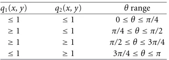
Table1: Octant location based on ratiosq1andq2.
q1(x, y) q2(x, y) θrange
≤1 ≤1 0≤θ≤π/4
≥1 ≤1 π/4≤θ≤π/2
≥1 ≥1 π/2≤θ≤3π/4
≤1 ≥1 3π/4≤θ≤π
a new capability for the DMG based on directional structur-ing elements. The angle estimation error for the DMG will be shown to be similar to that of the Sobel operator, and the four-component DMG will offer additional features not available from the two-component Sobel operator. When the two components atπ/4 and 3π/4 are added to the DMG, the orientation can be determined over a range of−π/2≤θ ≤
π/2 rather than just over one quadrant. However a rising edge and falling edge at the same orientation will still not be distinguished. For imaging relative to wafer defect de-tection and isolation, this ambiguity is not a problem. Let the gradient component ratiosq1andq2be defined by (12). The octant of the angle can be determined based on whether each ratio is greater than or less than one, as summarized in Table 1, and arctangents can be used to determine the angle value
Although the orientation estimates for the constant gra-dient model will always be correct, the results for an ideal step edge will have variability depending on the location of the edge relative to the pixel grid. The ideal step edge is modeled as an abrupt localized change in value defined by (13),
The angle of the edge isθand the distance of the edge from the origin of the coordinate system isd. The step edge can be interpreted as a thresholded ramp from the definition of (11). Unlike the constant gradient case, the acquired digi-tal image f(x, y) is not the same ass(x, y) due to the blur-ring of the sharp edges by the aperture function. In addi-tion, the edge response here will depend on the coordinatesx
andyand will be strongest at coordinates close to the abrupt change. Figure 2b shows the ideal step edge of Figure 2a af-ter blurring by an aperture of width 7. Figure 2d shows the gradient of the blurred edge computed using the DMG.
When the Sobel operator is used on f(x, y), an edge at a specific orientation can generate a range of values for the edge magnitude and orientation. This range will depend on
ρ, the distance of the edge from to the pixel center. For flat apertures of about one pixel in size, the error in the So-bel orientation estimate for an ideal step edge is limited to roughly 3◦. Figure 3 shows the orientation error from the Sobel operator for the ideal step edge with position offsets ofρ =0.0, 0.25, and 0.5 pixel widths relative to the nearest pixel center. Figure 3a shows results for a circular aperture of radius=0.707 pixel widths and Figure 3b shows the same re-sults for a circular aperture with a radius of one pixel width. A straight edge with an orientation ofθ typically will have individual pixel length segments which have offsets from the nearest pixel center spanning the full range possible. When the aperture size is known, a table lookup method could re-duce the error for edges withρ =0.0, but a table could not compensate for estimate variations due to variations in the value ofρalong the edge. As the amount of blurring increases due to convolution of the step edge image source with a larger aperture function, the ideal edge will have an extended area of gradual change and less localization.
Using the DMG instead of the Sobel operator, compen-sation for variations due to edge position offsets can be made with the four-component morphological gradient method [34] using a small table and interpolation. For very sharp edges with no added noise, this table can also be used to es-timate the relative position of the ideal edge and the pixel center. When the length of the one-dimensional filters is 3, a reasonable estimate of the angle can be made by averag-ing the arctangents ofq1andq2. This is shown in Figure 4 where it can be seen that the error is limited to 4.5◦. It is significant that these angle errors are so similar to the Sobel angle errors shown in Figure 3 because the basic morpholog-ical gradient provides no orientation information. By using a two-dimensional table lookup for a known aperture and interpolation rather than the average of the arctangents, the DMG angle error can theoretically be reduced as much as de-sired by adding more data to the table. However, other factors such as added noise will still limit accuracy.
Since two different estimates of the orientation are avail-able, inconsistency in the estimates can be used to reject some noise that creates false edges [32, 33, 34]. Thus, some edge segments with a significant gradient magnitude can be re-jected as noise if the two estimates are not compatible. Con-sider for example an impulsive noise sample on a constant amplitude background. This will result in both q1 and q2 having the same values, which is not consistent with an edge. In a similar fashion, gradients from a checkerboard pattern would also be rejected for inconsistency.
3.3. Addition of low pass and median filters
The Sobel and Prewitt operators use separable filters for each gradient component which perform a three-coefficient smoothing in the direction perpendicular to the differenc-ing filter direction. The Robert’s cross filter can also be inter-preted in a similar way for a 2×2 neighborhood rather than a 3×3 neighborhood. Since these operations are linear, the order of the smoothing and difference operations does not matter. By definition, the morphological gradient methods
−0.5
Figure3: Angle estimation error for the Sobel operator for an ideal edge acquired with a flat circular aperture of radiusr =0.707 (a) andr=1.00 (b). In both figures the solid line represents an ideal edge passing through the pixel center, while the dotted curve repre-sents an edge offset from the pixel center by one quarter of a pixel width, and the dot-dash curve represents an offset of half of a pixel width.
include only a difference operation, and performance might be improved by adding smoothing either before or after the difference is taken. The effect of smoothing operations used with morphological gradients will depend both on the or-der in which the smoothing and differencing are done and also on whether the smoothing uses a linear filter or a me-dian filter. A class of morphological filters with linear post smoothing is called DMGF [34].
−0.5
Figure4: Angle estimation error for the DMG operator of length 3 using the average arctangent for the same edges and apertures shown in Figure 3. In both figures the solid line represents an ideal edge passing through the pixel center, while the dotted curve repre-sents an edge offset from the pixel center by one quarter of a pixel width, and the dot-dash curve represents an offset of half of a pixel width.
aperture function of the image acquisition system. For the constant gradient model linear smoothing with a symmetric filter will not change the function. The effect of increasing the aperture for the step edge has already been discussed and demonstrated in Section 3.2. A median filter applied to ei-ther edge model will not change the function since both edge models are either monotonically nondecreasing or moniton-ically nonincreasing in any direction. Thus, the value at the center will always be the median value. Smoothing filters may also be applied after the DMG. The monotonic behavior of both edge models causes the length 3 DMG to produce the same result as the differencing part of the Sobel operator.
Thus linear post filtering applied to DMG results from either edge model could reproduce the Sobel or Prewitt smoothing operations. However, the DMG can also use longer structur-ing elements and larger filters. A one-dimensional median filter applied to the DMG results for either model will not change the output.
For defect detection and isolation from the design pat-tern, filters designed to attenuate the design pattern relative to the defect have been used [2]. For design pattern structures that are about four pixels in width, this type of smoothing filter would be much larger than the three pixel width Sobel filter. It will be shown in the next section that although such filters do suppress the design pattern to some extent, they do not provide reliable separation of the defect and the design. The defect is also blurred by the filtering, and, as a result, its edge strength is distributed over a fixed spatial interval. However, the DMG responds to difference anywhere within a fixed length defined by its SE, rather than to fixed spatial frequency. This allows the DMG to detect the larger irregu-lar defects more effectively than the Sobel operator after an initial smoothing operation has been applied to the images. The next section will demonstrate this capability on several examples and Section 5 will use analytical methods and ad-ditional examples to determine the range of effectiveness of the method.
4. APPLICATION TO DEFECT IMAGES
Several 256×256 sections of larger inspection images were analyzed using the directional morphological gradients and results were compared to other well-known methods. Al-though the pixels were represented by 8 bits, only 6 or 7 bits were needed for the full range of values used. The defects shown here are due to scratches and particles, but the miss-ing pattern defect images have characteristics similar to the particle defects. The objective of the processing is to separate the defects from the expected design pattern without a priori knowledge of the design details. It is assumed that the sur-face image of a design pattern free of defects would consist primarily of horizontal and vertical edges with sharp bound-aries or arrays of connection points. Lines in the design are expected to be about four pixels in width in the inspection images to provide adequate resolution for the design inspec-tion. In contrast, the defects are assumed to have random ori-entations with less distinct boundaries and irregular shapes and sizes.
(a) (b) (c)
(d) (e) (f)
Figure5: Three images showing defects on design patterns (a), (b), and (c) and the magnitudes of the corresponding two-dimensional Fourier transforms (d), (e), and (f).
(a) (b) (c) (d)
Figure6: Images from Figure 5 after smoothing. Images (a) and (b) are Figure 5b after smoothing by a 7×7 and a 15×15 uniform average, respectively. Images (c) and (d) are Figure 5c after smoothing by a 7×7 and a 15×15 uniform average.
same as those associated with connection points or the edges of the design pattern.
By viewing the corresponding spatial frequency domain images shown in the lower half of Figure 5, it is also clear that there is no reasonable spatial frequency separation be-tween the spot defects and the design pattern. Low pass fil-tering will reduce the high frequency components, but this will blur both the design pattern edges and the defect edges. This is confirmed by the images shown in Figure 6 in which 7×7 and 15×15 uniform averaging filters have been ap-plied to the images of Figures 5b and 5c. The design pattern is attenuated relative to the defect, but it is not completely eliminated. A comparison of the histograms of the original images and the smoothed images would show, as predicted, that the dynamic range of the intensity values is reduced by
the filtering operation. The scratch however is easily visible in the transform domain. The coherent edge at an unusual orientation is seen as a line through the origin of the trans-form domain at the angle corresponding to the gradient di-rection. Thus scratches should be detectable based on the ori-entation of the gradient responses as long as the scratches are not aligned with the horizontal or vertical pattern directions.
(a) (b) (c)
Figure7: Canny edge detector output after 7×7 averaging of images from Figure 5.
(a) (b) (c) (d)
(e) (f) (g) (h)
Figure8: Comparison of methods for particle or spot detection. Images from processing Figure 5b are shown in (a), (b), (c), and (d) and images from processing Figure 5c are shown in (e), (f), (g), and (h). On the left a smoothing filter of size 7×7 was used by the Sobel operator (a), (e) and the DMG7 (b), (f). On the right a smoothing filter of 15×15 was used by the Sobel operator (c), (g) and the DMG7 (d), (h).
is not sufficient. When the Canny edge detector is applied to the images shown in Figures 5a, 5b, and 5c almost all of the design features and defect features are identified. How-ever, the edges belonging to the design pattern cannot be easily separated from the edges belonging to the defect. Af-ter smoothing the original images with a 7×7 filter, applica-tion of the Canny edge detector creates the results shown in Figure 7. Figure 7a has lost some design detail relative to the unfiltered version, which is not shown, but the scratches are still present, and Figure 7b has lost only a small amount of design detail due to the image smoothing filter. In Figure 7c, there is no way to distinguish design edges from defect edges. When the size of the smoothing filter is doubled to 15×15, there is even less possibility of separating the defects from
the design based on edges. The scratch is almost completely lost and only the most distinct design features remain in the scratch image. Similar experiments with the well-known So-bel edge detector showed even worse results.
blurred further. The characteristic that distinguishes the de-fect is that it is larger, but not predictable in size compared to the design features. Because of this, after smoothing the larger extent of the defect edge makes a stronger contribu-tion to the morphological gradient than to the Sobel gradi-ent compongradi-ents. By using a morphological gradigradi-ent filter to find the maximum difference over a region regardless of the spatial separations within the region, the defect edges will be stronger than the design pattern edges. In contrast, an oper-ator such as the Sobel operoper-ator, which is defined by spatial frequency response, cannot make this distinction.
This process is demonstrated in Figure 8 for the two im-ages shown in Figures 5b and 5c. The imim-ages were created by computing the magnitude of the gradient and then thresh-olding the result at a level determined by the dynamic range of the input image and the size of the filters. The image in-tensity scale was then reversed so that darker values corre-spond to higher values of the gradient magnitude. Prior to edge detection, the images on the left were smoothed using a 7×7 pixel filter. The magnitude of the Sobel edge detector results were thresholded to produce Figures 8a and 8e. These results are almost indistinguishable from using a DMG with a length of 3 instead of the Sobel operator. However, when a DMG with length 7 is used instead, as shown in Figures 8b and 8f, the design pattern is greatly reduced compared to the defect boundary. The same procedure was repeated to pro-duce the images on the right, except that the prefilter used a 15×15 smoothing filter in place of a 7×7 smoothing filter. Using the DMG with a length of 7, as shown in Fig-ures 8d and 8h, retains the defects and suppresses the design pattern.
The histograms of the intensity values of the gradient images prior to thresholding, which are shown in Figure 9, clearly demonstrate that the morphological gradient pro-duces a wider range of intensity values than the Sobel opera-tor. All the images produced by the Sobel operator in Figure 8 all used a threshold level of 7. In Figures 8c and 8g this re-sulted in some loss of the defect definition while parts of the design pattern remain. Increasing the threshold causes addi-tional loss of both the defect and the design pattern. There is no threshold for the two Sobel images which completely sup-presses the design pattern while leaving a recognizable and measurable portion of the defect. The images produced by the DMG all used a threshold of 20, but a reasonable varia-tion of this level does not cause much change in the images. If the DMG threshold level is increased by 20% from 20 to 24, all of the design pattern is still suppressed. There is a small loss of definition of the defects so that they are similar to the defects shown in the Sobel results with the best threshold in Figures 8c and 8g. If the DMG threshold is reduced by 20% to 16, the defect image becomes stronger and the amount of undesired design pattern that is present is similar to that of the best threshold for Sobel operator results shown in Figures 8c and 8g. It should be noted that these threshold values were determined by the properties of the input data range and the filter definitions, not by the shape of the histogram. A similar variation of 20% in the threshold value for the Sobel operator does not produce usable results.
0 10 20 30 40 50 60
Figure 9: Pixel intensity histograms for the gradient images that were thresholded to create the corresponding images in Figure 8.
−200−150−100−50 0 50 100 150 200
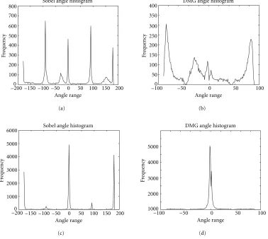
Figure10: Histogram of orientations detected for the Sobel operator and the DMG3 operator (a) and (c) are histograms that Sobel edge orientation applied to image from Figures 5a and 5b. (b) and (d) are histograms that DMG3 edge orientation applied to image from Figures 5a and 5b.
first approach might accept individual edge segments only if their orientations were not near the horizontal and ver-tical lines of the design pattern and then examine the re-sulting image for remaining long lines. This method was not successful. It effectively erased most of the horizontal and vertical design pattern lines, but it also took out some of the edge segments associated with the scratch because the scratch has an irregular edge boundary. What was left was a scratch that had an edge strength similar to the weak horizontal and vertical edges and to all the other parts of the design pattern that had any curvature. Thus, in the re-sulting image the edge of the scratch was not easily sepa-rated from the design pattern. Further, when this method was applied to the images from Figures 5b and 5c, which do not have scratches, there was a significant residue of edge elements that exceeded the amount left in the scratch image.
Detection of the scratch requires the detection of a co-herent set of edge segments with similar orientation, so de-tection from a histogram of image edge orientations will be more effective. Figure 10 shows histograms of the orientation of edge segments when the Sobel operator and the DMG3
operator are applied to the images of Figure 5a, which has a scratch, and Figure 5b which does not. Note that the Sobel operator identifies the edge orientation over all four quad-rants while the DMG3 specifies the orientation only within a two-quadrant range. All of the histograms show the ex-pected strong response due to horizontal and vertical lines from the design pattern. However, in the upper plots of Figure 10, which came from the scratch image of Figure 5a, the histograms also show an additional strong peak due to the scratch. Once this peak has been located in the tion histogram, edge segments near that particular orienta-tion can be separated and the scratch can be located using a Radon or Hough transform [26].
0
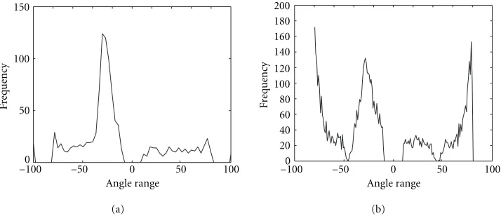
Figure11: Histograms from Figures 10a and 10b, respectively, after removal of horizontal and vertical edges.
(a)
Figure12: Orientation histogram (b) and modified histogram (c) for the image with a scratch shown in (a).
for the angle estimate are available from the early processing stages and require no additional computation.
For comparison, the image from Figure 5b was used to generate the lower histograms of Figure 10. These histograms show identifiable peaks for the horizontal lines and a much smaller peak for the vertical lines. The remaining edge seg-ments associated with the spot and the connection points in the image are distributed relatively evenly over all of the angles. Although the image has a significant number of edge segments which are not horizontal or vertical, there is no in-dication of a peak which could be misinterpreted as a scratch. This method is effective for the location of scratches which are not aligned with the axes of the design pattern and which are long enough to generate a detectable concentration of edge segments at the orientation angle of the scratch.
The peaks of the angle histograms can be found using conventional histogram peak finding techniques, but for pur-poses of scratch detection, it is only necessary to detect a coherent edge at an angle that is not 0 nor 90 degrees. A number of peak detection techniques will find the peaks associated with the scratch in Figures 10a and 10b. One simple method would compute a coarse histogram with 10 degree wide bins and a 5 degree overlap. Any angle with
a population significantly above the floor value would be considered a coherent edge. The classic peak detection meth-ods usually start with a lowpass filter applied to smooth the histogram. Then the first order derivative or gradient is used for the one-dimensional histogram array. Correspond-ing zero-crossCorrespond-ing points are taken as peak points. Once peak points are located, a sorting process in terms of voting num-ber will be used to find higher peaks and lower peaks. With the orientation information of the design pattern, the peak of the orientation for the defects can be found. Since the angle estimated for a scratch will typically represent a small range of angles, tolerance factors will be used to group them together.
from Figure 10, the modified histogram with horizontal and vertical gradients removed shows a clear peak associated with the scratch, while the gradients associated with the circular pattern structures are spread over all angles.
5. PERFORMANCE EVALUATION
Performance of the DMG demonstrated in the previous sec-tion can be predicted based on models of the images of the design pattern structures and defects. It has been assumed that the image acquisition process will produce design pat-tern components with a pixel dimension of approximately three or four so that the design pattern can be observed in the image. A smoothing filter that would significantly attenuate the variability due to the design pattern should have a mini-mum size of twice the feature dimension, so a 7×7 smooth-ing filter was tested first. However, the periodicity of the array of design elements is also important, and a larger smoothing filter of 15×15 would be expected to cause greater attenua-tion. Smoothing filters of size 7, 15, and 21 are investigated.
For this analysis it is useful to define a rectangular func-tion rect(x), which has a value of 1 for −0.5 < x ≤ 0.5 and is 0 elsewhere. A vertical pattern stripe of infinite height and width a centered atx = xc can be written as
f(x, y) = rect((x −xc)/a) while a square aperture func-tion of size b centered at the origin can be written as
s(x, y)=(1/b)2rect(x/b) rect(y/b). Consider a stripe defined by f1(x, y)= A rect((x−xc)/a) blurred bys(x, y). The re-sulting blurred stripe has a trapezoidal intensity pattern with a central width of (1 +|b−a|) and a complete width of (a+b−1). The slope on the rising and falling edges of the trapezoid has a magnitude of (A/b) per pixel, and for allb
larger than a, the maximum value in the central width is
Aa/b. Thus, asb increases, the value of both the slope and the central maximum decrease. The Sobel operator will have a response of 2/bfor a unit height stripe of width 3 or larger, while the DMG7 will have a response ofa/bfor a unit height stripe of widtha <7 and a response of 7/bfora >7.
The same blurring will be applied to defects as well as the pattern structures. However, the DMG can respond to the maximum difference over a range defined by the struc-turing element, while a linear operator like the Sobel oper-ator responds only to difference at fixed spatial separations. This allows the DMG to have a stronger response to the de-fect than the Sobel operator. Several examples of this effect on performance are shown in Figure 13. Each of the four defect images shown on the left is smoothed by a 15×15 filter. The gradient computed using the Sobel operator is shown in the center and the gradient computed using the DMG is shown on the right. The image defect in the top row has well-defined edges and appears on a design pattern with densely packed small features. In this case the smooth-ing filter suppresses most of the design pattern and both gra-dients show the boundary of the defect. The Sobel opera-tor result has a small amount of design pattern remaining. The second and third rows show less well-defined defects against a more open design pattern with larger features. In both cases, the gradient intensities computed by the Sobel
operator for the design pattern and for the defect had over-lapping values and could not be separated by thresholding. In contrast, the DMG produced nonoverlapping gradient in-tensities for the defect and the pattern which allowed sep-aration. It should be noted that the edge effects of the im-age processing, which frame the imim-ages, were left to facilitate alignment when most structures were suppressed. The fourth row shows a defect with very diffuse boundaries. The DMG gradient produces a more reliable boundary for it than the Sobel operator, but both methods miss the lightest part of the defect edge.
In Figure 14, the effect of increasing the size of the smoothing filter is explored. The results from the two ex-amples in the middle of Figure 13 are shown with gradient magnitudes computed after smoothing by a 7×7 filter on the left, by a 15×15 filter in the center, and by a 21×21 fil-ter on the right. In both examples, the DMG performs well for all three filter sizes, though the edges of the defect start to break up for the largest filter. For the 7×7 filter, the Sobel operator retains a significant amount of the design pattern structure. For the 21×21 filter, most of the design pattern is suppressed but the defect boundary is also diminished. This demonstrates that the DMG gives more reliable performance than the Sobel operator over a wider range of input and im-age processing variability.
Figures 15 and 16 show two examples that are problem-atic for both the Sobel operator and the DMG. The first ex-ample shows a very small defect against a high contrast pat-tern structure. The DMG is better able to separate it from the design than the Sobel operator, but some definition of the defect is lost. The second example shows a very diffuse defect with very little contrast compared to the background. The higher contrast design pattern dominates the defect for both methods over all three filter sizes.
6. CONCLUSION
(a) (b) (c)
(d) (e) (f)
(g) (h) (i)
(j) (k) (l)
Figure13: Four images of defects are shown on the left (a), (d), (g), and (j). After smoothing with a 15×15 filter, gradient detection by the Sobel operator is shown in the center (b), (e), (h), and (k), and gradient detection by the DMG7 is shown on the right (c), (f), (i) , and (l).
sufficient resolution that design features span three or four pixels.
The same directional morphological gradient methods used to detect the particle defects can also be used to de-tect a large number of scratch defects. This application uses the orientation information that was added to the basic mor-phological gradient by using small one-dimensional struc-turing elements. Since the new directional morphological
(a)
(b)
(c)
(d)
Figure14: Defect images from Figures 13d and 13g processed by Sobel operator and DMG7 after using smoothing prefilters of size 7×7 (left), 15×15 (center), and 21×21 (right). The results for Figure 13d are shown in (a) for the Sobel operator and (b) for the DMG7. The results for Figure 13g are shown in (c) for the Sobel operator and (d) for the DMG7.
(a) (b) (c) (d)
(a)
(b)
(c)
(d)
Figure16: Defect images from Figures 15a and 15c processed by Sobel operator and DMG7 after using smoothing prefilters of size 7×7 (left), 15×15 (center), and 21×21 (right). The results for Figure 15a are shown in (a) for the Sobel operator and (b) for the DMG7. The results for Figure 15c are shown in (c) for the Sobel operator and (d) for the DMG7.
information about connectivity of the edge segments. Also nonrectangular structures such as connection points will not cause problems with the scratch detection histogram. Their edge segments will have orientation values distributed over the full range of angles. For design patterns which have sig-nificant edges that are not horizontal or vertical, specific ex-clusion of these particular angles would also be necessary.
The new directional morphological gradient method presented in this paper uses the basic operations of
REFERENCES
[1] M. Lemke, J. Wienecke, M. Graf, and D. Albrecht, Defect in-spection philosophy, Jenoptik Technologies GMBH, Jena, Ger-many, 2001.
[2] L. F. Pau, Computer Vision for Electronics Manufacturing, Plenum Press, New York, NY, USA, 1990.
[3] A. Braun, “Defect detection overcomes limitations,” Semicon-ductor International, vol. 22, no. 2, pp. 44–52, 1999.
[4] J. Baliga, “Defect detection on patterned wafers,” Semicon-ductor International, pp. 64–70, May 1997.
[5] P. Burggraaf, “Remarkable trends in wafer inspection,” Semi-conductor International, pp. 57–60, December 1994.
[6] N. Chang, “Submicron defect detection by SEMSpec: an e-beam wafer inspection system,” inMachine Vision Applica-tions in Industrial Inspection VII, vol. 3652 ofSPIE Proceedings, pp. 94–99, March 1999.
[7] D. Grelinger, “Submicron defect detection standard for pat-terned wafer inspection systems,” inIntegrated Circuit Metrol-ogy, Inspection, and Process Control VI, vol. 1673 ofSPIE Pro-ceedings, pp. 506–514, June 1992.
[8] P. Sandland, “Automated defect inspection: past, present, and future,” inMetrology, Inspection, and Process Control for Mi-crolithography XII, vol. 3332 ofSPIE Proceedings, pp. 296–308, June 1998.
[9] M. Altamirano and A. Skumanich, “Enhanced defect de-tection capability using combined brightfield/darkfield imag-ing,” inIn-Line Characterization Techniques for Performance and Yield Enhancement in Microelectronic Manufacturing II, vol. 3509 ofSPIE Proceedings, pp. 60–64, August 1998. [10] R. Cappel and J. Rathert, “The advantages of in-line
electron-beam wafer inspection,” Yield Management Solutions, vol. 2, no. 3, pp. 8–12, 2000.
[11] A. Braun, “Defect inspection enters integration era,” Semi-conductor International, vol. 24, no. 8, pp. 142–154, 2001. [12] B. Choo, T. Riley, B. Schulz, and B. Singh, “Improving process
control for 0.18 um technology and beyond,” Yield Manage-ment Solutions, vol. 2, no. 3, pp. 55–58, 2000.
[13] Z. Abraham, “SEM defect review and classification for semi-conductor device manufacturing,” inMetrology-Based Con-trol for Micro-Manufacturing, vol. 4275 ofSPIE Proceedings, pp. 99–106, June 2001.
[14] T. Esposito, M. Barns, S. Morell, and E. Wang, “Automatic defect classification : a productivity improvement tool,”Yield Management Solutions, vol. 1, no. 2, pp. 29–33, 1998. [15] L. Breaux and D. Kolar, “Automatic defect classification for
effective yield management,” Solid State Technology, vol. 39, no. 12, pp. 89–96, 1996.
[16] B. Singh, L. Wagner, and S. Riley, “Automatic defect classifi-cation for effective yield management,” Semiconductor Inter-national, pp. 103–114, March 1997.
[17] G. Stinson and B. Magluyan, “Application of automatic defect classification in photolithography,” Yield Management Solu-tions, vol. 2, no. 3, pp. 27–31, 2000.
[18] B. Hance, I. Ne’eman, and A. Skumanich, “Enhanced defect capture and analysis based on automatic defect classification at post-lithographic inspection,” inMetrology, Inspection, and Process Control for Microlithography XIV, vol. 3998 ofSPIE Proceedings, pp. 732–737, June 2000.
[19] M. Kulkarni and A. Skumanich, “Yield enhancement based on defect reduction using on-the-fly automatic defect clas-sification,” inMetrology, Inspection, and Process Control for Microlithography XIV, vol. 3998 ofSPIE Proceedings, pp. 686– 693, June 2000.
[20] F. Lakhani and W. Tomlinson, “SEM-based automatic defect classification (ADC),” inIn-Line Methods and Monitors for Process and Yield Improvement, vol. 3884 ofSPIE Proceedings, pp. 306–313, August 1999.
[21] A. Skumanich, “Process and yield improvement based on fast in-line automatic defect classification,” inIn-Line Methods and Monitors for Process and Yield Improvement, vol. 3884 of SPIE Proceedings, pp. 278–289, August 1999.
[22] A. Skumanich and M.-P. Cai, “CMP process development based on rapid automatic defect classification,” inIn-Line Characterization, Yield Reliability, and Failure Analyses in Mi-croelectronic Manufacturing, vol. 3743 ofSPIE Proceedings, pp. 76–88, April 1999.
[23] M. Bennett, K. Tobin, and S. Gleason, “Automatic defect clas-sification: status and industry trends,” inIntegrated Circuit Metrology, Inspection, and Process Control IX, vol. 2439 ofSPIE Proceedings, pp. 210–220, May 1995.
[24] P. Chou, A. Rao, M. Sturzenbecker, and V. Brecher, “Auto-matic defect classification for integrated circuits,” inMachine Vision Applications in Industrial Inspection, vol. 1907 ofSPIE Proceedings, pp. 95–103, May 1993.
[25] R. Sherman, E. Tirosh, and Z. Smilansky, “Automatic defect classification system for semiconductor wafers,” inMachine Vision Applications in Industrial Inspection, vol. 1907 ofSPIE Proceedings, pp. 72–79, May 1993.
[26] W. Pratt, Digital Image Processing, John Wiley & Sons, New York, NY, USA, 2nd edition, 1991.
[27] E. R. Davies, Machine Vision: Theory, Algorithms, Practicali-ties, Academic Press, London, UK, 1990.
[28] R. C. Gonzalez and R. E. Woods, Digital Image Processing, Addison-Wesley, New York, NY, USA, 2nd edition, 1992. [29] R. M. Haralick and L. G. Shapiro,Computer and Robot Vision,
Addison-Wesley, Reading, Mass, USA, 1993.
[30] F. van der Heijden, Image Based Measurement Systems, John Wiley & Sons, Chichester, UK, 1994.
[31] E. R. Dougherty,An Introduction to Morphological Image Pro-cessing, SPIE Press, Bellingham, Wash, USA, 1992.
[32] S. Wood and G. Qu, “A modified gray level morphologi-cal gradient with accurate orientation estimates and reduced noise sensitivity,” inProc. 34th IEEE Asilomar Conf. on Signal, System, and Computers, October 2000.
[33] G. Qu and S. Wood, “Performance of a modified gray level morphological gradient with low sensitivity to threshold val-ues and noise,” inProc. 34th IEEE Asilomar Conf. on Signal, System, and Computers, October 2000.
[34] G. Qu,Directional morphological gradient edge detector, Ph.D. thesis, Computer Engineering, Santa Clara University, July 2001.
[35] D. Marr, Vision, W. H. Freeman, San Francisco, Calif , USA, 1982.
[36] J. Canny, “A computational approach to edge detection,”IEEE Trans. on Pattern Analysis and Machine Intelligence, vol. 8, no. 6, pp. 679–698, 1986.
[37] J. Serra, Image Analysis and Mathematical Morphology, Aca-demic Press, London, UK, 1982.
[38] J. Lee, R. M. Haralick, and L. G. Shapiro, “Morphological edge detector,” IEEE Trans. Robotics and Automation, vol. 3, no. 2, pp. 142–153, 1987.
Gongyuan Qureceived his B.S. and M.S. degrees in computer engineering from the Harbin Institute of Technology, China, in 1982 and 1985, respectively, and Ph.D. de-gree in computer engineering from Santa Clara University in 2002. As a software prin-cipal engineer and part-time researcher, he has worked with several Silicon Valley com-panies on development of image processing and machine vision software, IC diagnostic
tools, defect inspection machines, and defect image and IC yield management systems. His research interests include machine vi-sion, image processing, industrial defect detection and database ap-plication to image analysis.
Sally L. Woodreceived her B.S. in electrical
engineering from Columbia University School of Engineering in 1969 and her M.S. and Ph.D. degrees in electrical engineering from Stanford University in 1974 and 1978, respectively. Prior to joining the faculty at Santa Clara University in 1985, she worked for several companies designing hardware and algorithms for machine recognition of printed characters and image segmentation
of CT and MRI images for three-dimensional model construction. At Santa Clara University, she has continued research in signal and image processing with applications to communications systems, image understanding, and three-dimensional modeling from sequences of two-dimensional images. Dr. Wood has been active in IEEE conference organization and has held several elected positions in the IEEE Signal Processing Society. For the past six years, she has served as the Electrical Engineering Department Chair.
Cho Tehreceived his Ph.D. degree in
electri-cal engineering from the University of Wis-consin, Madison in 1988 and the master of engineering degree from the National Uni-versity of Singapore in 1982. He has worked in the areas of machine and computer vi-sion, image processing and pattern recog-nition, and signal processing. Over the past 20 years, he has worked on applications in the areas of wafer defect and mark