ISSN (Print) : 2320 – 3765 ISSN (Online): 2278 – 8875
I
nternational
J
ournal of
A
dvanced
R
esearch in
E
lectrical,
E
lectronics and
I
nstrumentation
E
ngineering
(An ISO 3297: 2007 Certified Organization)
Vol. 5, Issue 9, September 2016
Speed Control of DC Motor with Modified
SEPIC Rectifier
Greeshma Ann Sabu1, Tomson Thomas2
PG Student [PE], Dept. of EEE, St. Joseph’s College of Engineering and Technology, Palai, Kerala, India1 Assistant Professor, Dept. of EEE, St. Joseph’s College of Engineering and Technology, Palai, Kerala, India2
ABSTRACT: This paper proposes a new single-phase ac-dc power factor correction (PFC) bridgeless single ended primary inductor converter (SEPIC) rectifier with speed control of DC motor. It is used to improve the efficiency at low input voltage and reduce the switch-voltage stress. The absence of an input rectifier bridge in the SEPIC rectifier results in less conduction losses. Lower switch voltage stress allows utilizing a MOSFET. The topology is designed to operate in discontinuous conduction mode (DCM) to achieve almost a unity power factor. The DCM operation have advantages such as zero-current turn-on in the power switches and simple control circuitry. Speed control of the DC motor is done using this bridgeless SEPIC rectifier. Converter output is given to the input of the DC motor.
KEYWORDS:Power factor correction (PFC), bridgeless SEPICrectifier, DC motor, discontinuous current mode (DCM).
I.INTRODUCTION
Advantages of single ended primary inductor converter (SEPIC) circuit are isolation easy, EMI small and input current is continuous. The working principle of the different modes of the SEPIC-PFC areanalyzed. It is note that there are several problems in traditional circuit, such as the great loss of rectifier bridge structure, the reverse current recovery under continuous mode and so on. To solve the above mentioned problem, a new bridgeless SEPIC PFC circuit is presented.Based on traditional SEPIC power factor correction, new circuits utilize the bridgeless technique instead of the pre-rectifier in the corrector. In the process of turning on the switch, the input current only flow one diode, and it can effectively reduced energy consumption in the conduction process. The circuit works in the current DCM. The DCM operation results in soft turn-on switching and relatively low inrush current. The proposed bridgeless rectifier with coupled magnetic configurations results in higher overall efficiency and higher power density. The proposed topology has some advantages over the conventional SEPIC converter, such that the dc output voltage is lower than the peak input voltage, input–output isolation can be easily implemented.
II. SYSTEM MODEL AND WORKING
The proposed bridgeless power factor correction SEPIC converter with DC motor circuit is shown in Fig. 1. The proposed bridgeless configuration willreduce the conduction losses. The multiplier cell (D1, C3and D2, C3) will increase
the gain and reduce the switch voltage stress. The proposed circuit consists of two symmetrical configurations and each will operate in a half-line cycle. Circuit consists of ac input voltage; 2 switches: Q1 and Q2; 5 diodes D0, D1, D2, Dpand
Dn; 3 inductors: L0, L1 and L2; 3 capacitors: C0, C1 and C2 and the DC motor. By the two diodes Dpand Dn, the output
ground is always connected to the terminals of input ac voltage, which stabilizes voltage potential of output ground. The three separate inductors can be magnetically coupled into a single magnetic core to attain very low input current ripples. The proposed converter utilizes two non-floating switches, Q1 and Q2. SwitchQ1is turned ON/OFF during the
positive half-line cycle andthat of switch Q2is in negative half-line cycle. The two power switches Q1 and Q2can
Fig. 1. Proposed bridgeless PFC SEPIC rectifier fed DC motor.
The circuit operation during one switching period Tsin a positive half-line period with the three inductors operating in
DCM, can be divided into three distinct operating modes. They are:
MODE 1
Fig. 2.Mode 1- Switch ON topology.
The mode 1- switch ON topology is shown in Fig. 2. Switch Q1is turned-on by the control signal. Both the diodesD1
and D0 are reversed biased. In this stage, the three-inductor currents increase linearly at a rate proportional to the input
voltage Vac.
MODE 2
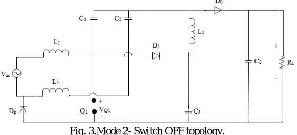
Fig. 3.Mode 2- Switch OFF topology.
The mode 2- switch OFF topology is shown in Fig. 3.Switch Q1is turned-off. Both the diodes D1 and D0 will conduct
simultaneously. These will provide a path for the currents of the three inductors. The three inductors’ currents decrease linearly at a rate proportional to the capacitor C1voltage VC1. This stage continues till the sum of the currents flowing in
ISSN (Print) : 2320 – 3765 ISSN (Online): 2278 – 8875
I
nternational
J
ournal of
A
dvanced
R
esearch in
E
lectrical,
E
lectronics and
I
nstrumentation
E
ngineering
(An ISO 3297: 2007 Certified Organization)
Vol. 5, Issue 9, September 2016
MODE 3
Fig. 4.Mode 3- DCM topology.
The mode 3- DCM topology is shown in Fig. 4.Switch Q1remains turned-off. Both the diodesD1 and D0 are reverse
biased. Diode Dpprovides a path for the current of the inductor L0. The three inductors behave as current sources, so
there will be constant currents. Thereby, the voltage across the three inductors is zero. This period ends when switch Q1is turned-on initiating the next turn-on of the switching cycle.
III. SIMULATION
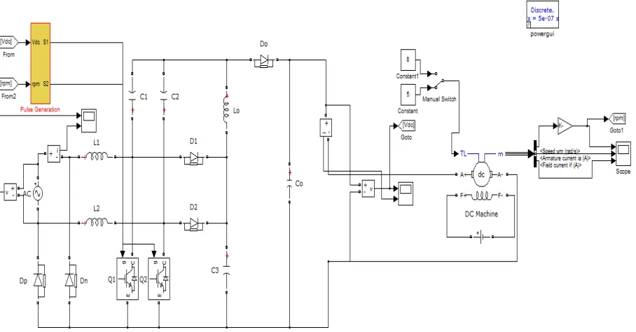
Fig. 5. Simulink model of the bridgeless PFC SEPIC converter fed DC motor.
Fig. 6. Gate pulses for the switches Q1and Q2.
Here the proposed SEPIC converter input voltage is taken as 120V ac. The output voltage is designed for 54V dc. The gate pulses generated for the switches Q1 and Q2 are shown in the Fig. 6. The simulation result of the power factor
obtained from the SEPIC rectifier is shown in the Fig. 7.
Fig. 7. Simulation result of the power factor obtained from the SEPIC rectifier.
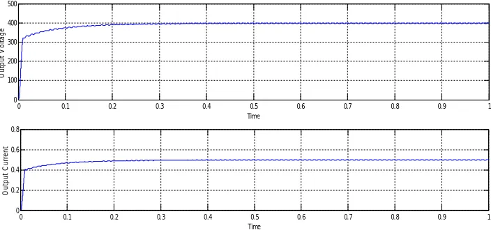
The switching frequency is 50kHz. Simulation results of output voltage and output current of the SEPIC rectifier are shown in Fig. 8. The output voltage obtained is 400V and output current obtained is 0.5A.
Fig. 8. Simulation results of output voltage and output current of the SEPIC rectifier.
0 0.1 0.2 0.3 0.4 0.5 0.6 0.7 0.8 0.9 1
0 100 200 300 400 500
Time
O
u
tp
u
t
V
o
lt
a
g
e
Output Voltage
0 0.1 0.2 0.3 0.4 0.5 0.6 0.7 0.8 0.9 1
0 0.2 0.4 0.6 0.8
Time
O
u
tp
u
t
C
u
rr
e
n
t
ISSN (Print) : 2320 – 3765 ISSN (Online): 2278 – 8875
I
nternational
J
ournal of
A
dvanced
R
esearch in
E
lectrical,
E
lectronics and
I
nstrumentation
E
ngineering
(An ISO 3297: 2007 Certified Organization)
Vol. 5, Issue 9, September 2016
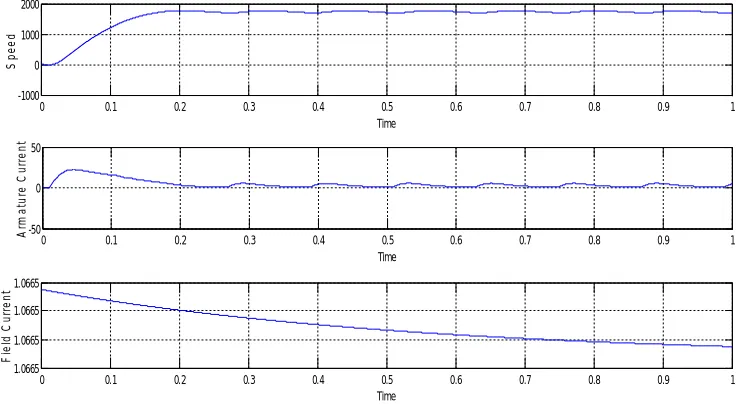
Simulation results of the speed, armature current, field current of the DC motor are shown in Fig. 9. The speed of the DC motor is obtained as around 1800 rpm and the armature current obtained almost as 0.1A.
Fig. 9. Simulation results of the speed, armature current, field current of the DC motor.
IV. HARDWARE IMPLEMENTATION
Hardware implementation of the proposed bridgeless PFC SEPIC rectifier fed DC motor is given in the Fig. 10. The hardware setup consists of SEPIC converter circuit, driver circuit, control circuit and DC motor. The driver circuit contains FAN7382 used as the IC for the MOSFET. The processor chosen is ATmega328P, which is a low-power CMOS 8-bit microcontroller.
Fig. 10. Hardware implementation of the bridgeless PFC SEPIC rectifier fed DC motor.
0 0.1 0.2 0.3 0.4 0.5 0.6 0.7 0.8 0.9 1
-1000 0 1000 2000 Time S p e e d Motor Speed
0 0.1 0.2 0.3 0.4 0.5 0.6 0.7 0.8 0.9 1
-50 0 50 Time A rm a tu re C u rr e n
t Armature Current
0 0.1 0.2 0.3 0.4 0.5 0.6 0.7 0.8 0.9 1
The result obtained from the hardware setup is given below. Hardware result of the gate pulses of the switches Q1and
Q2 is shown in Fig. 11.
Fig. 11. Hardware result of the gate pulses of the switches Q1and Q2.
V. RESULT AND DISCUSSION
The proposed bridgeless power factor correction SEPIC rectifier fed DC motor is shown in Fig. 1 and its modes, mode1-switch ON topology is shown in Fig. 2, mode 2-switch OFF topology is shown in Fig. 3 and mode 3-DCM topology is shown in Fig. 4. Simulink model of the proposed SEPIC rectifier fed DC motor is given in Fig. 5. The simulation results obtained are given in the Fig. 6, 7, 8 and 9. Then the hardware is implemented. Hardware setup of the proposed SEPIC rectifier fed DC motor is given in Fig. 10. The result obtained from the hardware setup is given in the Fig. 11.
VI.CONCLUSION
A single phase ac-dc bridgeless power factor correction SEPIC converter fed DC motor is proposed in this paper. The SEPIC converter output is given to the input of the DC motor. The DC motor is driven by the voltage 54V. The proposed bridgeless rectifier with coupled magnetic configurations results in higher overall efficiency and higher power density. The proposed topology has some advantages such that the dc output voltage is lower than the peak input voltage, input–output isolation can be easily implemented. Experimental results are provided to confirm the converter operation in reference to conventional SEPIC converter operation.
REFERENCES
[1] Ahmed M. Al Gabri, Abbas A. Fardoun and Esam H. Ismail,“Bridgeless PFC-Modified SEPIC Rectifier With Extended Gain for Universal Input Voltage Applications,” IEEE Trans. Power Electron., vol. 30, no. 8, pp.4272-4282, Aug. 2015.
[2] P. F. de Melo, R.Gules, E. F. Romaneli, and R.C.Annunziato, “Amodified SEPIC converter for high-power-factor rectifier and universal input voltage applications,” IEEE Trans. Power Electron., vol. 25, no. 2, pp. 310–321,Feb. 2010.
[3] M. Mahdavi and H. Farzanehfard, “Bridgeless SEPIC PFC rectifier with reduced components and conduction losses,” IEEE Trans. Ind. Electron.,vol. 58, no. 9, pp. 4153–4160, Sep. 2011.
[4] E. H. Ismail, “Bridgeless SEPIC rectifier with unity power factor and reduced conduction losses,” IEEE Trans. Ind. Electron., vol. 56, no. 4, pp. 1147–1157, Apr. 2009.
[5] J.-W. Yang and H.-L. Do, “Bridgeless SEPIC converter with a ripple-free input current,” IEEE Trans. Power Electron., vol. 28, no. 7, pp. 3388–3394, Jul. 2013.
[6] H. Wang, Y. Tang, and A. Khaligh, “A bridgeless boost rectifier for low voltage energy harvesting applications,” IEEE Trans. Power Electron.,vol. 28, no. 11, pp. 5206–5214, Nov. 2013.
ISSN (Print) : 2320 – 3765 ISSN (Online): 2278 – 8875
I
nternational
J
ournal of
A
dvanced
R
esearch in
E
lectrical,
E
lectronics and
I
nstrumentation
E
ngineering
(An ISO 3297: 2007 Certified Organization)
Vol. 5, Issue 9, September 2016
[8] Y. Jang and M. Jovanovic, “A Bridgless PFC boost rectifier with optimized magnetic utilization,” IEEE Trans. Power Electron., vol. 24, no. 1, pp. 85–93, Jan. 2009.
[9] K. Yao, X. Ruan, X. Mao, and Z. Ye, “Reducing storage capacitor of a DCM boost PFC converter,” IEEE Trans. Power Electron., vol. 27, no. 1, pp. 151–160, Jan. 2012.
[10] A. A. Fardoun, E. H. Ismail, A. J. Sabzali, andM.A.Al-Saffar, “Acomparison between three proposed bridgeless Cuk topologies and conventional topologies for power factor correction,” IEEE Trans. Power Electron., vol. 27, no. 7, pp. 3292–3301, Jul. 2012.
[11] A. Abramovitz and K. M. Smedley, “Analysis and design of a tappedinductor buck–boost PFC rectifier with low bus voltage,” IEEE Trans. Power Electron., vol. 26, no. 9, pp. 2637–2649, Sep. 2011.
[12] A. Fardoun, E. Ismail, A. Sabzali, and M. Al-Saffar, “Bridgeless resonant pseudo boost PFC rectifier,” IEEE Trans. Power Electron., vol. 29, no. 11, pp. 5949–5960, Nov. 2014.
[13] Y. Kim, W. Sung, and B. Lee, Comparative performance analysis of high density and efficiency PFC topologies,” IEEE Trans. Power Electron., vol. 29, no. 6, pp. 2666–2679, Jun. 2014.